

Page 1
FAN6754A
Highly Integrated Green- Mode PWM Controller
FAN6754A — Highly Integrated Green-Mode PWM Controller
April 2012
Brownout and V
Adjustment by HV Pin
Limit
Features
High-Voltage Startup
AC Input Brownout Protection with Hysteresis
Monitor HV to Adjust V
Limit
Low Operating Current: 1.5mA
Linearly Decreasing PWM Frequency to 22KHz
Frequency Hopping to Reduce EMI Emission
Fixed PWM Frequency: 65KHz
Peak-Current-Mode Control
Cycle-by-Cycle Current Limiting
Leading-Edge Blanking (LEB)
Internal Open-Loop Protection
GATE Output Maximum Voltage Clamp: 13V
V
V
Under-Voltage Lockout (UVLO)
DD
Over-Voltage Protection (OVP)
DD
Programmable Over-Temperature Protection (OTP)
Internal Latch Circuit (OVP, OTP)
Open-Loop Protection (OLP); Restart for MR, Latch
for ML
SENSE Short-Circuit Protection (SSCP)
Built-in 8ms Soft-Start Function
Applications
General-purpose switch-mode power supplies and
flyback power converters, including:
Power Adapters
Description
The highly integrated FAN6754A PWM controller
provides several features to enhance the performance
of flyback converters. To minimize standby power
consumption, a proprietary green-mode function
provides off-time modulation to continuously decrease
the switching frequency under light-load conditions.
Under zero-load and very light-load conditions,
FAN6754A saves PWM pulses by entering deep burst
mode. This burst mode function enables the power
supply to meet international power conservation
requirements.
FAN6754A integrates a frequency-hopping function
internally to reduce EMI emission of a power supply with
minimum line filters. Built-in synchronized slope
compensation is accomplished by proprietary HV
monitor to adjust V
over universal AC input range. The gate output is
clamped at 13V to protect the external MOSFET from
over-voltage damage.
Other protection functions include AC input brownout
protection with hysteresis, SENSE pin short-circuit
protection, and V
temperature protection, an external NTC thermistor can
be applied to sense the external switcher’s temperature.
When V
circuit is used to latch-off the controller. The latch mode
is reset when the V
FAN6754A is available in an 8-pin SOP package.
OVP or OTP are activated, an internal latch
DD
for constant output power limit
Limit
over-voltage protection. For over-
DD
supply is removed.
DD
Related Resources
Evaluation Board: FEBFAN6754AMR_CP450v1
Ordering Information
Part Number
FAN6754AMRMY
FAN6754AMLMY
© 2011 Fairchild Semiconductor Corporation www.fairchildsemi.com
FAN6754A • Rev. 1.0.3
Operating
Temperature Range
-40 to +105°C 8-Pin, Small Outline Package (SOP) Tape & Reel
Package Packing Method
Page 2
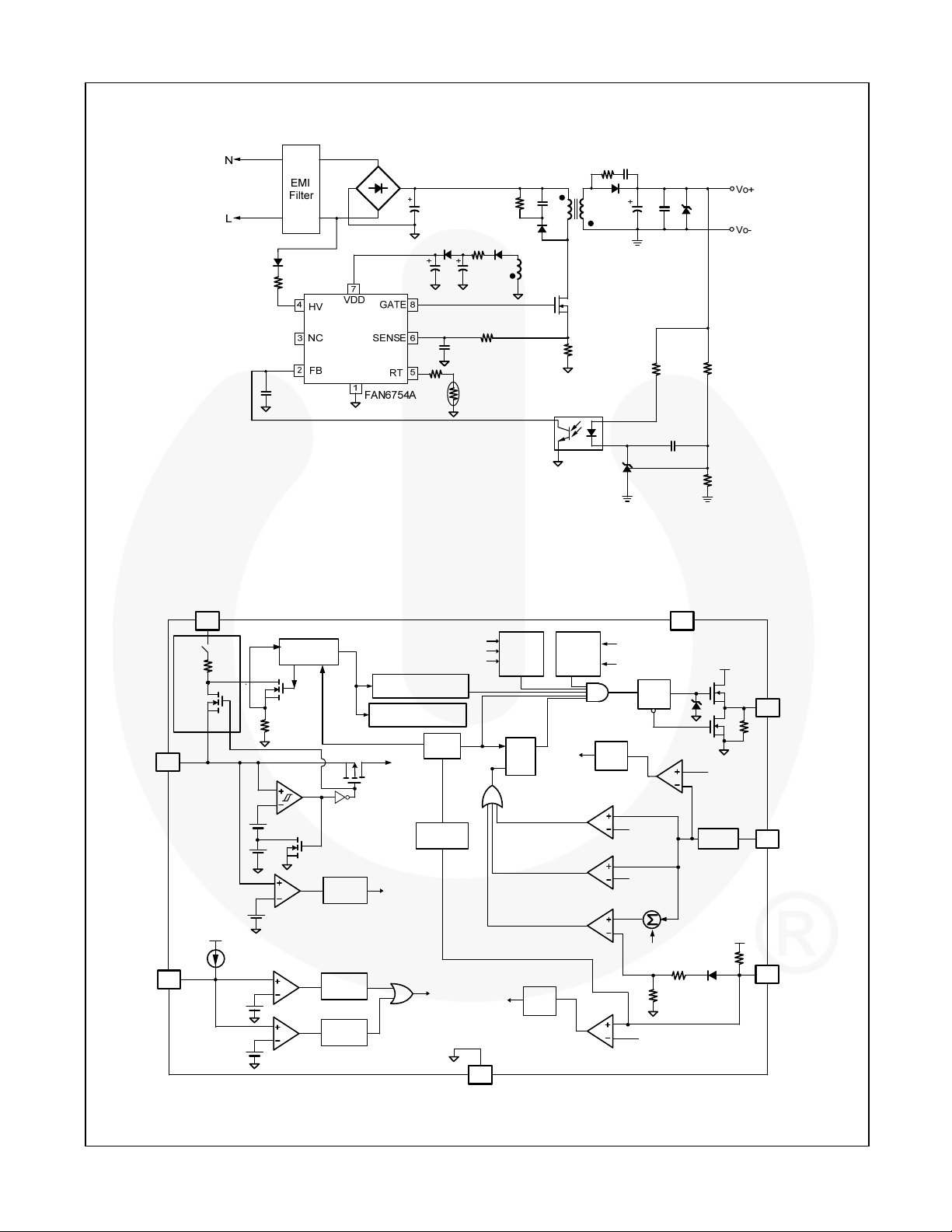
Application Diagram
FAN6754A — Highly Integrated Green-Mode PWM Controller
Internal Block Diagram
4 3
Line Voltage
Sample Circuit
HV
Startup
VDD
7
UVLO
17V/10V
V
DD-OVP
I
RT
RT
5
1.05V
0.7V
Figure 1. Typical Application
OVP
Latch
OTP
OLP for ML
Protection
Brownout Protection
V
Adjustment
Limit
Debounce
t
D-OTP1
Counter
t
D-OTP2
Counter
Internal
BIAS
OVP
OSC
Green
Mode
OTP
OLP
QS
R
Delay
1
GND
Figure 2. Functional Block Diagram
Re-Start
Protection
SSCP
Soft-Start
Comparator
Current Limit
Comparator
PWM
Comparator
OLP
Comparator
OLP
SSCP
Delay
SSCP
OLP for MR
Soft
Driver
SSCP
Comparator
Soft-Start
V
Limit
Slope
Compensation
R
4.6V
NCHV
GATE
8
0.05V
Circuit
Blanking
5V
3R
6
2
SENSE
FB
© 2011 Fairchild Semiconductor Corporation www.fairchildsemi.com
FAN6754A • Rev. 1.0.3 2
Page 3
A
A
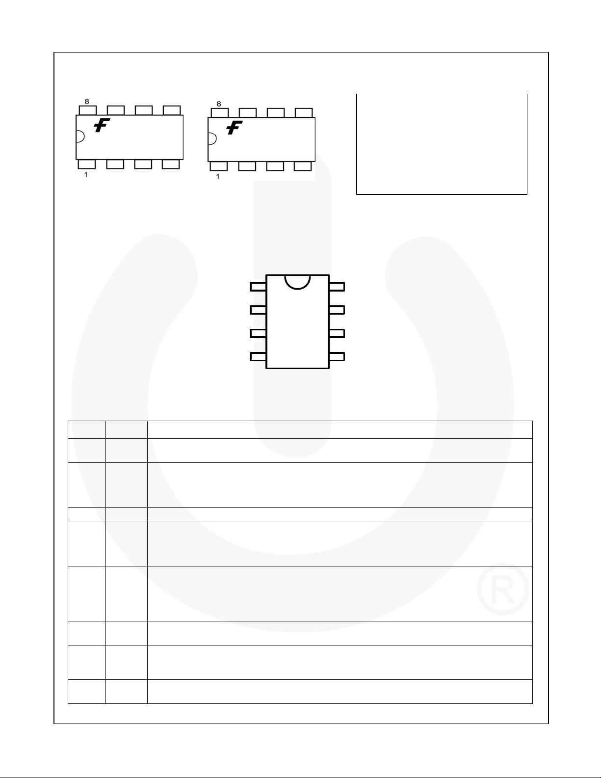
Marking Information
ZXYTT
6754MR
TPM
Pin Configuration
ZXYTT
6754ML
TPM
Figure 3. Top Mark
SOP-8
FAN6754A — Highly Integrated Green-Mode PWM Controller
F - Fairchild Logo
Z - Plant Code
X - 1-Digit Year Code
Y - 1-Digit Week Code
TT - 2-Digit Die Run Code
T - Package Type (M=SOP)
P - Y: Package (Green)
M - Manufacture Flow Code
Pin Definitions
Pin # Name Description
1 GND
2 FB
3 NC
4 HV
5 RT
6 SENSE
7 VDD
8 GATE
Ground. This pin is used for the ground potential of all the pins. A 0.1µF decoupling capacitor
placed between VDD and GND is recommended.
Feedback. The output voltage feedback information from the external compensation circuit is fed
into this pin. The PWM duty cycle is determined by this pin and the current-sense signal from Pin
6. FAN6754A performs open-loop protection (OLP); if the FB voltage is higher than a threshold
voltage (around 4.6V) for more than 56ms, the controller latches off the PWM.
No Connection
High-Voltage Startup. This pin is connected to the line input via a 1N4007 and 200kΩ resistor to
achieve brownout and high/low line compensation. Once the voltage on the HV pin is lower than
the brownout voltage, PWM output turns off. High/low line compensation dominates the cycle-bycycle current limiting to achieve constant output power limiting with universal input.
Over-Temperature Protection. An external NTC thermistor is connected from this pin to GND.
The impedance of the NTC decreases at high temperatures. Once the voltage on the RT pin
drops below the threshold voltage, the controller latches off the PWM. If RT pin is not connected
to NTC resistor for Over-Temperature Protection, a 100KΩ series one resistor is recommended
to ground to prevent from noise interference. This pin is limited by an internal clamping circuit.
Current Sense. This pin is used to sense the MOSFET current for the current-mode PWM and
current limiting.
Supply Voltage. IC operating current and MOSFET driving current are supplied using this pin.
This pin is connected to an external bulk capacitor of typically 47µF. The threshold voltages for
turn-on and turn-off are 17V and 10V, respectively. The operating current is lower than 2mA.
Gate Drive Output. The totem-pole output driver for the power MOSFET. It is internally clamped
below 13V.
GND
FB
NC
HV
Figure 4. Pin Configuration (Top View)
18
2
3
7
6
54
GATE
VDD
SENSE
RT
© 2011 Fairchild Semiconductor Corporation www.fairchildsemi.com
FAN6754A • Rev. 1.0.3 3
Page 4
FAN6754A — Highly Integrated Green-Mode PWM Controller
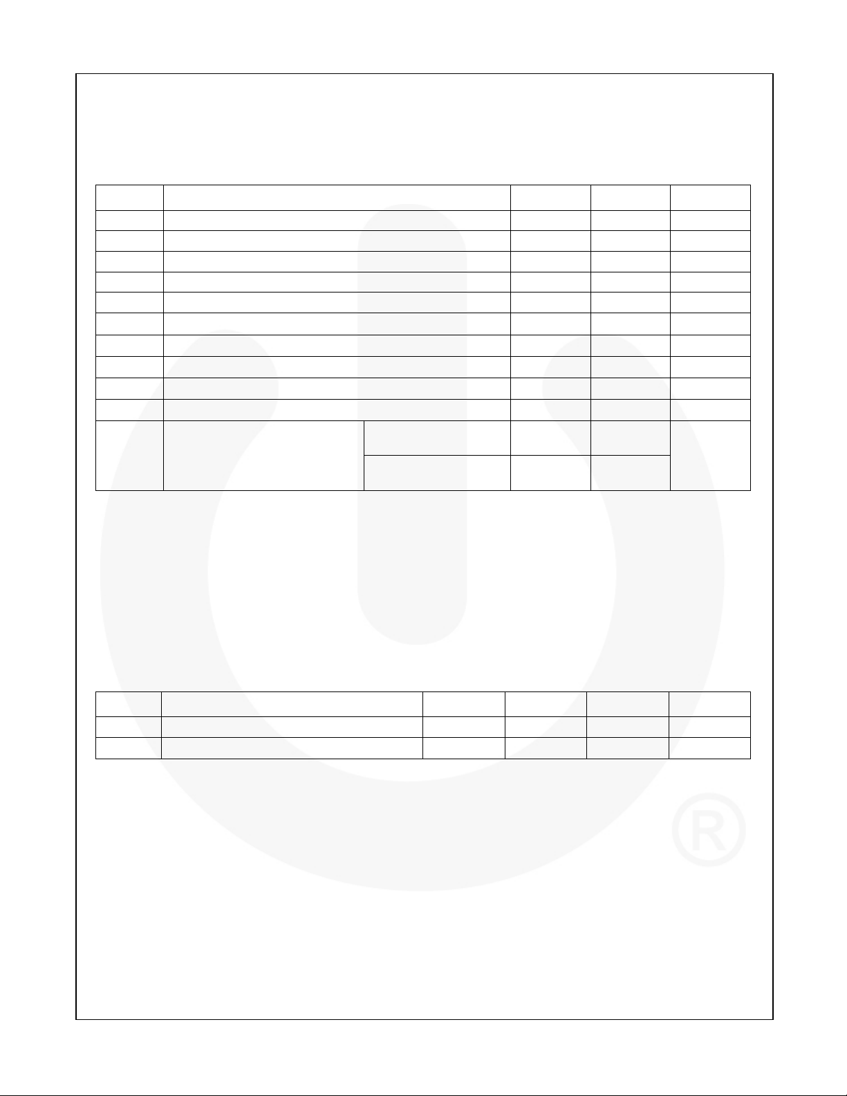
Absolute Maximum Ratings
Stresses exceeding the absolute maximum ratings may damage the device. The device may not function or be
operable above the recommended operating conditions and stressing the parts to these levels is not recommended.
In addition, extended exposure to stresses above the recommended operating conditions may affect device reliability.
The absolute maximum ratings are stress ratings only.
Symbol Parameter Min. Max. Unit
V
DC Supply Voltage
VDD
VFB FB Pin Input Voltage -0.3 7.0 V
V
SENSE Pin Input Voltage -0.3 7.0 V
SENSE
VRT RT Pin Input Voltage -0.3 7.0 V
VHV HV Pin Input Voltage 500 V
PD
ΘJA
Power Dissipation (T
Thermal Resistance (Junction-to-Air) 150
TJ Operating Junction Temperature -40 +125
T
Storage Temperature Range -55 +150
STG
TL Lead Temperature (Wave Soldering or IR, 10 Seconds) +260
ESD
Electrostatic Discharge Capability,
All Pins Except HV Pin
Notes:
1. All voltage values, except differential voltages, are given with respect to the network ground terminal.
2. Stresses beyond those listed under Absolute Maximum Ratings may cause permanent damage to the device.
3. ESD with HV pin: CDM=1000V and HBM=500V.
(1,2)
30 V
<50°C)
A
400 mW
°C/W
°C
°C
°C
Human Body Model;
JESD22-A114
Charged Device Model;
JESD22-C101
4500
V
1500
Recommended Operating Conditions
The Recommended Operating Conditions table defines the conditions for actual device operation. Recommended
operating conditions are specified to ensure optimal performance to the datasheet specifications. Fairchild does not
recommend exceeding them or designing to Absolute Maximum Ratings.
Symbol Parameter Min. Typ. Max. Unit
TA Operating Ambient Temperature -40 +105 °C
RHV HV Startup Resistor 150 200 250
kΩ
© 2011 Fairchild Semiconductor Corporation www.fairchildsemi.com
FAN6754A • Rev. 1.0.3 4
Page 5
FAN6754A — Highly Integrated Green-Mode PWM Controller
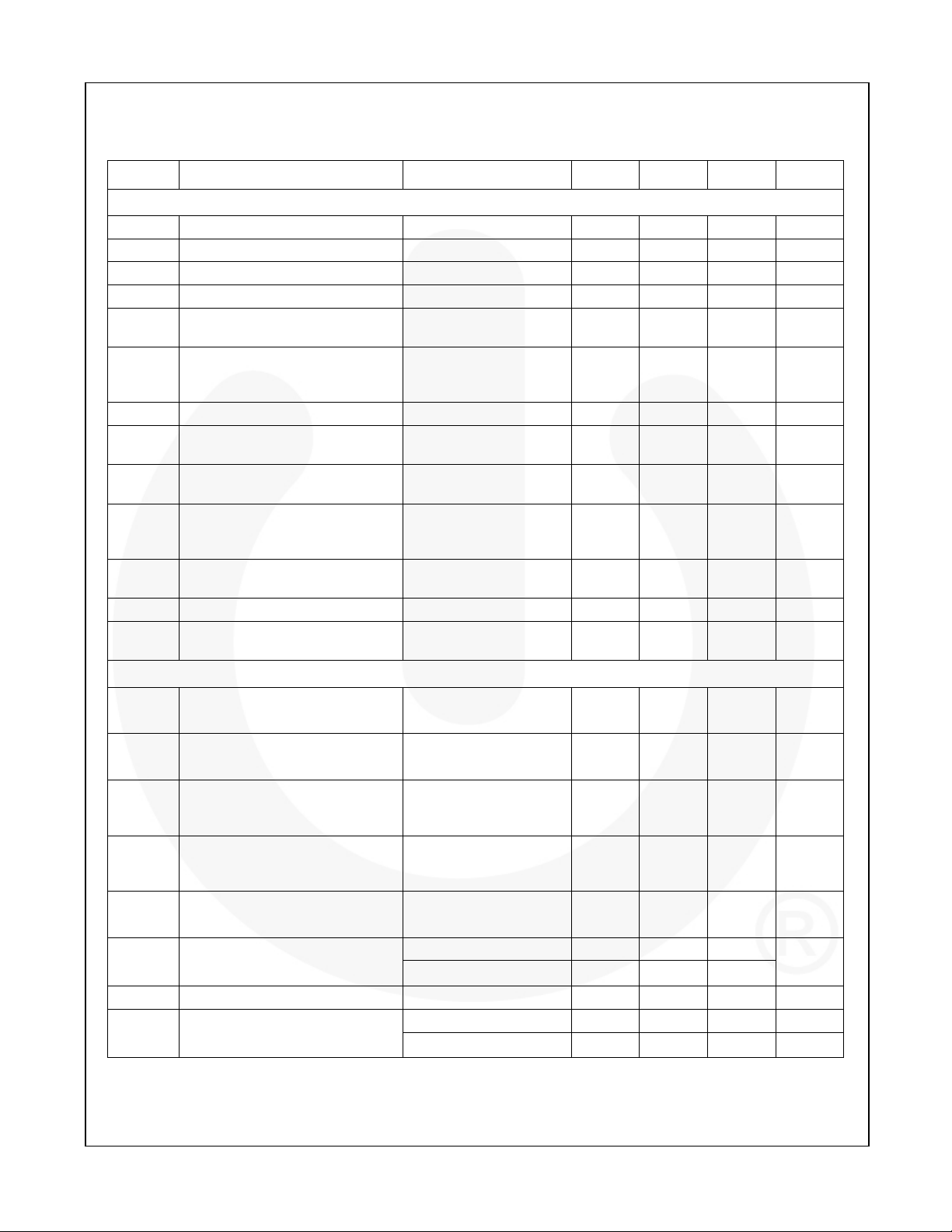
Electrical Characteristics
VDD=15V and TA=25°C unless otherwise noted.
Symbol Parameter Conditions Min. Typ. Max. Units
VDD Section
VOP Continuously Operating Voltage 24 V
V
Start Threshold Voltage 16 17 18 V
DD-ON
V
Minimum Operating Voltage 9 10 11 V
DD-OFF
V
I
DD-OLP
V
DD-LH
V
DD-AC
I
Startup Current V
DD-ST
I
DD-OP1
I
DD-OP2
ILH
I
DD-OLP
V
V
DD-OVP
t
D-VDDOVP
HV Section
Off Voltage 5.5 6.5 7.5 V
DD-OLP
Threshold Voltage on VDD Pin for
Latch-Off Release Voltage
Threshold Voltage on VDD Pin for
Disable AC Recovery to Avoid
Startup Failed
Operating Supply Current,
PWM Operation
Operating Supply Current,
Gate Stop
3.5 4.0 4.5 V
V
– 0.16V 30 µA
DD-ON
=20V, FB=3V Gate
V
DD
DD-OFF
+2.8
Open
V
DD-OFF
+3.3
V
DD-OFF
+3.8
1.5 2.0 mA
VDD=20V, FB=3V 1.0 1.5 mA
Operating Current at PWM-Off
Phase Under Latch-Off
VDD=5V 30 60 90 µA
Conduction
Internal Sink Current Under LatchOff Conduction
Over-Voltage Protection 24 25 26 V
DD
Over-Voltage Protection
V
DD
Debounce Time
+0.1V
V
DD-OLP
75 165 255 µs
170 200 230 µA
V
=90V(VDC=120V),
V
IHV Supply Current from HV Pin
I
Leakage Current after Startup
HV-LC
AC
V
=0V
DD
HV=700V, V
+1V
OFF
DD=VDD-
2.0 3.5 5.0 mA
1 20 µA
DC Source Series
V
Brownout Threshold
AC-OFF
R=200kΩ to HV Pin
92 102 112 V
See Equation 1
DC Source Series
V
Brownin Threshold
AC-ON
R=200kΩ to HV Pin
104 114 124 V
See Equation 2
V
ΔVAC
t
Line Voltage Sample Cycle
S-CYCLE
t
Line Voltage Hold Period 20 µs
H-TIME
t
PWM Turn-off Debounce Time
D-AC-OFF
AC-ON
- V
AC-OFF
DC Source Series
R=200kΩ to HV Pin
FB > V
FB < V
FB > V
FB < V
220
FB-N
650
FB-G
65 75 85 ms
FB-N
180 235 290 ms
FB-G
6 12 18 V
Continued on page the following page…
µs
© 2011 Fairchild Semiconductor Corporation www.fairchildsemi.com
FAN6754A • Rev. 1.0.3 5
Page 6

FAN6754A — Highly Integrated Green-Mode PWM Controller
Figure 5. Brownout Circuit
V
IN-ON
V
IN-OFF
V
IN
Gate
Gate start
Brownout debounce time
Figure 6. Brownout Behavior
Gate stop
Figure 7. V
© 2011 Fairchild Semiconductor Corporation www.fairchildsemi.com
FAN6754A • Rev. 1.0.3 6
and AC Recovery
DD-AC
Page 7
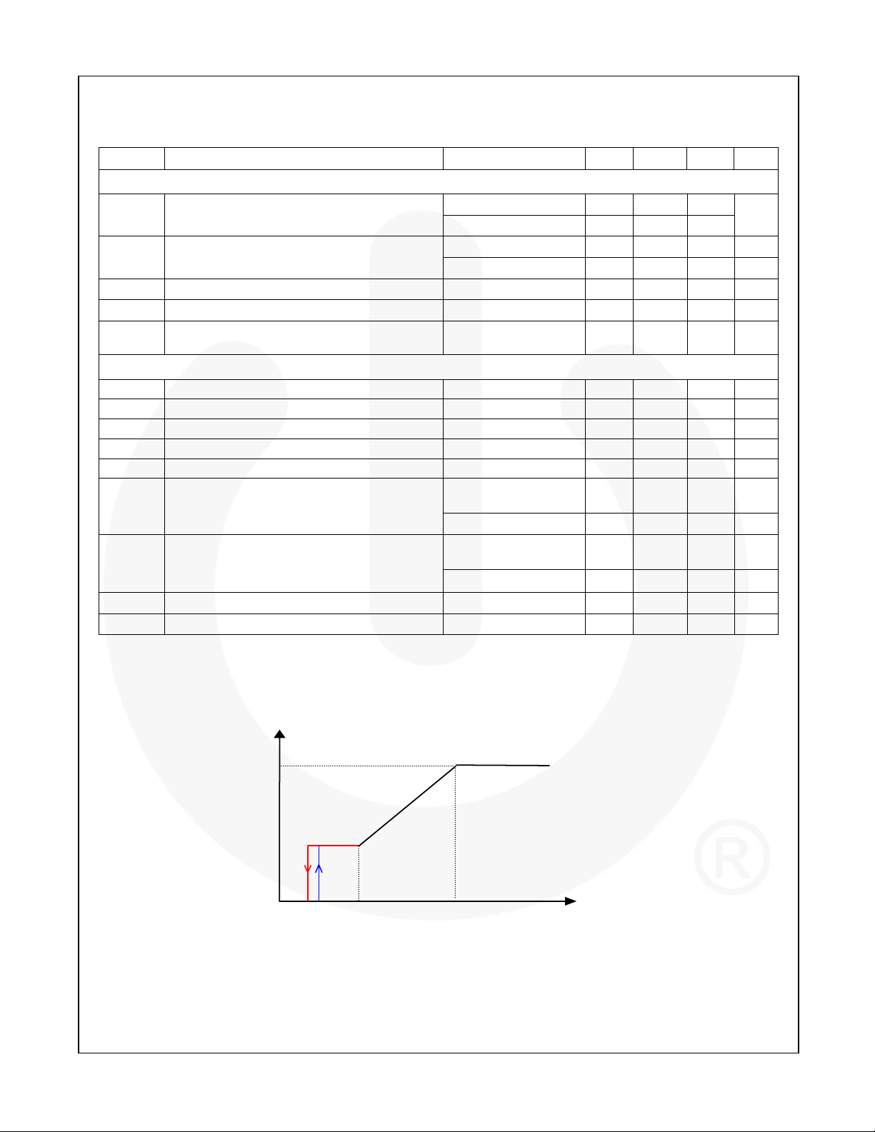
Electrical Characteristics (Continued)
VDD=15V and TA=25°C unless otherwise noted.
Symbol Parameter Conditions Min. Typ. Max. Units
Oscillator Section
f
Frequency in Normal Mode
OSC
t
Hopping Period
HOP
f
Green-Mode Frequency 19 22 25 KHz
OSC-G
Center Frequency
Hopping Range ±3.7 ±4.2 ±4.7
FB > VFB-N 3.9 4.4 4.9 ms
FB=VFB-G 10.2 11.5 12.8 ms
fDV Frequency Variation vs. VDD Deviation VDD=11V to 22V 5 %
61 65 69
KHz
FAN6754A — Highly Integrated Green-Mode PWM Controller
fDT Frequency Variation vs. Temperature Deviation
T
=-40 to +105°C
A
5 %
Feedback Input Section
AV Input Voltage to Current-Sense Attenuation 1/4.5 1/4.0 1/3.5 V/V
ZFB Input Impedance 14 16 18 kΩ
V
V
V
V
Output High Voltage FB Pin Open 4.8 5.0 5.2 V
FB-OPEN
FB Open-Loop Trigger Level 4.3 4.6 4.9 V
FB-OLP
t
Delay Time of FB Pin Open-Loop Protection 50 56 62 ms
D-OLP
Pin, FB Voltage
(FB
=V
)
V
Green-Mode Entry FB Voltage
FB-N
FB-N
Hopping Range
Pin, FB Voltage
V
Green-Mode Ending FB Voltage
FB-G
(FB =V
FB-G
)
Hopping Range
FB Threshold Voltage for Zero-Duty Recovery 1.9 2.1 2.3 V
FB-ZDCR
FB Threshold Voltage for Zero-Duty 1.8 2.0 2.2 V
FB-ZDC
2.6 2.8 3.0 V
±3.7 ±4.2 ±4.7
2.1 2.3 2.5 V
±1.27 ±1.45 ±1.62
Continued on the following page…
PWM Frequency
f
OSC
f
OSC-G
V
FB-ZDC
V
FB-ZDCR
Figure 8. V
V
FB-G
V
FB-N
vs. PWM Frequency
FB
V
FB
kHz
kHz
© 2011 Fairchild Semiconductor Corporation www.fairchildsemi.com
FAN6754A • Rev. 1.0.3 7
Page 8
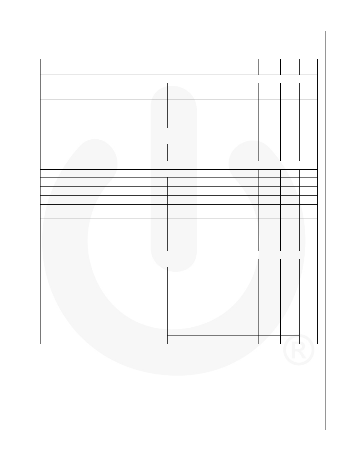
Electrical Characteristics (Continued)
VDD=15V and TA=25°C unless otherwise noted.
Symbol Parameter Conditions Min. Typ. Max. Unit
s
Current-Sense Section
tPD Delay to Output 100 250 ns
t
Leading-Edge Blanking Time 230 280 330 ns
LEB
V
=122V, Series R=200kΩ
V
Current Limit at Low Line (VAC=86V)
Limit-L
V
Current Limit at High Line (VAC=259V)
Limit-H
V
Threshold Voltage for SENSE Short-Circuit Protection 0.03 0.05 0.07 V
SSCP
t
On Time for V
ON-SSCP
t
Delay for SENSE Short-Circuit Protection
D-SSCP
Checking 4.0 4.4 4.8 µs
SSCP
tSS Soft-Start Time Startup Time 7 8 9 ms
GATE Section
DCY
I
GATE-SINK
Maximum Duty Cycle 86 89 92 %
MAX
V
Gate Low Voltage
GATE-L
V
Gate High Voltage
GATE-H
Gate Sink Current
I
GATE-
SOURCE
V
GATE-
CLAMP
Gate Source Current
tr
Gate Rising Time V
tf
Gate Falling Time V
Gate Output Clamping Voltage V
(4)
(4)
RT Section
IRT Output Current from RT Pin 92 100 108 µA
V
RTTH1
V
RTTH2
t
D-OTP1
Over-Temperature Protection Threshold
Voltage
Over-Temperature Latch-Off Debounce
t
D-OTP2
Note:
4. Guaranteed by design.
DC
to HV
=366V, Series R=200kΩ
V
DC
to HV
<0.05V
V
SENSE
=15V, IO=50mA
V
DD
=12V, IO=50mA
V
DD
=15V
V
DD
=15V, GATE=6V
V
DD
=15V, CL=1nF 100
DD
=15V, CL=1nF 50
DD
=22V 9 13 17
DD
0.7V < V
< 1.05V, after
RT
12ms Latch Off
< 0.7V, After 100µs
V
RT
Latch Off
V
RTTH2
FB > V
V
RTTH2
FB < V
VRT< V
VRT< V
< VRT < V
FB-N
< VRT < V
FB-G
, FB > V
RTTH2
, FB < V
RTTH2
RTTH1
RTTH1
110 185 260
FB-N
320 605 890
FB-G
0.43 0.46 0.49 V
0.36 0.39 0.42 V
60 120 180 µs
1.5 V
8 V
300 mA
250 mA
ns
ns
V
1.000 1.035 1.070
V
0.65 0.70 0.75
14 16 18
ms
40 51 62
µs
FAN6754A — Highly Integrated Green-Mode PWM Controller
© 2011 Fairchild Semiconductor Corporation www.fairchildsemi.com
FAN6754A • Rev. 1.0.3 8
Page 9

Typical Performance Characteristics
FAN6754A — Highly Integrated Green-Mode PWM Controller
Figure 9. Startup Current (I
Figure 11. Start Threshold Voltage (V
vs. Temperature
) vs. Temperature
DD-ST
DD-ON
)
Figure 10. Operation Supply Current (I
vs. Temperature
Figure 12. Minimum Operating Voltage (V
vs. Temperature
DD-OP1
DD-OFF
)
)
Figure 13. Supply Current Drawn from HV Pin (IHV)
vs. Temperature
Figure 15. Frequency in Normal Mode (f
vs. Temperature
© 2011 Fairchild Semiconductor Corporation www.fairchildsemi.com
FAN6754A • Rev. 1.0.3 9
OSC
)
Figure 14. HV Pin Leakage Current After Startup
(I
) vs. Temperature
HV-LC
Figure 16. Maximum Duty Cycle (DCY
vs. Temperature
MAX
)
Page 10
Typical Performance Characteristics (Continued)
FAN6754A — Highly Integrated Green-Mode PWM Controller
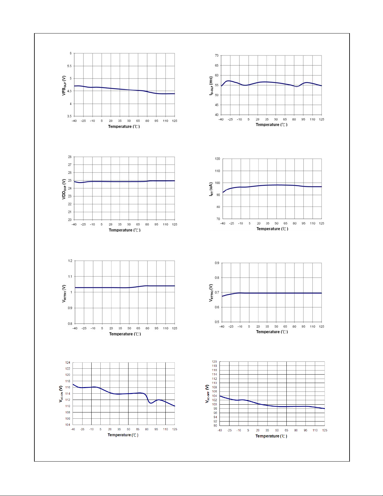
Figure 17. FB Open-Loop Trigger Level (V
vs. Temperature
Figure 19. VDD Over-Voltage Protection (V
vs. Temperature
FB-OLP
DD-OVP
)
)
Figure 18. Delay Time of FB Pin Open-Loop
Protection (t
) vs. Temperature
D-OLP
Figure 20. Output Current from RT Pin (IRT)
vs. Temperature
Figure 21. Over-Temperature Protection Threshold
Voltage (V
Figure 23. Brownin (V
© 2011 Fairchild Semiconductor Corporation www.fairchildsemi.com
FAN6754A • Rev. 1.0.3 10
) vs. Temperature
RTTH1
) vs. Temperature Figure 24. Brownout (V
AC-ON
Figure 22. Over-Temperature Protection Threshold
Voltage (V
) vs. Temperature
RTTH2
AC-OFF
) vs. Temperature
Page 11

Functional Description
FAN6754A — Highly Integrated Green-Mode PWM Controller
Startup Current
For startup, the HV pin is connected to the line input
through an external diode and resistor; R
, (1N4007 /
HV
200KΩ recommended). Peak startup current drawn from
the HV pin is (V
capacitor through the diode and resistor. When the V
capacitor level reaches V
switches off. At this moment, the V
supplies the FAN6754A to keep the V
× 2 ) / RHV and charges the hold-up
AC
, the startup current
DD-ON
capacitor only
DD
until the
DD
DD
auxiliary winding of the main transformer provides the
operating current.
Operating Current
Operating current is around 1.5mA. The low operating
current enables better efficiency and reduces the
requirement of V
hold-up capacitance.
DD
Green-Mode Operation
The proprietary green-mode function provides off-time
modulation to reduce the switching frequency in lightload and no-load conditions. V
, which is derived from
FB
the voltage feedback loop, is taken as the reference.
Once V
is lower than the threshold voltage (V
FB
FB-N
), the
switching frequency is continuously decreased to the
minimum green-mode frequency of around 22KHz.
Current Sensing / PWM Current Limiting
Peak-current-mode control is utilized to regulate output
voltage and provide pulse-by-pulse current limiting. The
switch current is detected by a sense resistor into the
SENSE pin. The PWM duty cycle is determined by this
current-sense signal and V
, the feedback voltage.
FB
When the voltage on the SENSE pin reaches around
V
= (VFB–0.6)/4, the switch cycle is terminated
COMP
immediately. V
is internally clamped to a variable
COMP
voltage around 0.46V for low-line output power limit.
Leading-Edge Blanking (LEB)
Each time the power MOSFET is switched on, a turn-on
spike occurs on the sense-resistor. To avoid premature
termination of the switching pulse, a leading-edge
blanking time is built in. During this blanking period, the
current-limit comparator is disabled and cannot switch
off the gate driver.
Under-Voltage Lockout (UVLO)
The turn-on and turn-off thresholds are fixed internally at
17V and 10V, respectively. During startup, the hold-up
capacitor must be charged to 17V through the startup
resistor to enable the IC. The hold-up capacitor
continues to supply V
delivered from auxiliary winding of the main transformer.
V
must not drop below 10V during startup. This UVLO
DD
hysteresis window ensures that hold-up capacitor is
adequate to supply V
until the energy can be
DD
during startup.
DD
Gate Output / Soft Driving
The BiCMOS output stage is a fast totem-pole gate
driver. Cross conduction has been avoided to minimize
heat dissipation, increase efficiency, and enhance
reliability. The output driver is clamped by an internal
13V Zener diode to protect power MOSFET transistors
against undesirable gate over voltage. A soft driving
waveform is implemented to minimize EMI.
Soft-Start
For many applications, it is necessary to minimize the
inrush current at startup. The built-in 8ms soft-start
circuit significantly reduces the startup current spike and
output voltage overshoot.
Slope Compensation
The sensed voltage across the current-sense resistor is
used for peak-current-mode control and cycle-by-cycle
current limiting. Built-in slope compensation improves
stability and prevents sub-harmonic oscillation.
FAN6754A inserts a synchronized, positive-going, ramp
at every switching cycle.
Constant Output Power Limit
When the SENSE voltage across sense resistor R
reaches the threshold voltage, around 0.46V for low-line
condition, the output GATE drive is turned off after a
small delay, t
current proportional to t
. This delay introduces an additional
PD
• VIN / LP. Since the delay is
PD
nearly constant regardless of the input voltage V
higher input voltage results in a larger additional current
and the output power limit is higher than under low input
line voltage. To compensate this variation for a wide AC
input range, a power-limiter is controlled by the HV pin
to solve the unequal power-limit problem. The power
limiter is fed to the inverting input of the current limiting
comparator. This results in a lower current limit at highline inputs than at low-line inputs.
Brownout and Constant Power Limited by
the HV Pin
Unlike previous PWM controllers, FAN6754A’s HV pin
can detect the AC line voltage brownout function and
adjust the current limit. Using a fast diode and startup
resistor to sample the AC line voltage, the peak value
refreshes and is stored in a register at each sampling
cycle. When internal update time is met, this peak value
is used for brownout and current-limit level judgment.
Equation 1 and 2 calculate the level of brownin or
brownout converted to RMS value. For power saving,
FAN6754A enlarges the sampling cycle to lower the
power loss from HV sampling at light-load condition.
ON- AC
OFF- AC
where R
is in kΩ.
HV
+
1.6) (R
HV
×=
0.9V ( (RMS) V
1.6
1.6) (R
+
HV
0.81V ( (RMS) V
×=
1.6
2 / )
2 / )
SENSE
IN
(1)
(2)
,
© 2011 Fairchild Semiconductor Corporation www.fairchildsemi.com
FAN6754A • Rev. 1.0.3 11
Page 12
FAN6754A — Highly Integrated Green-Mode PWM Controller
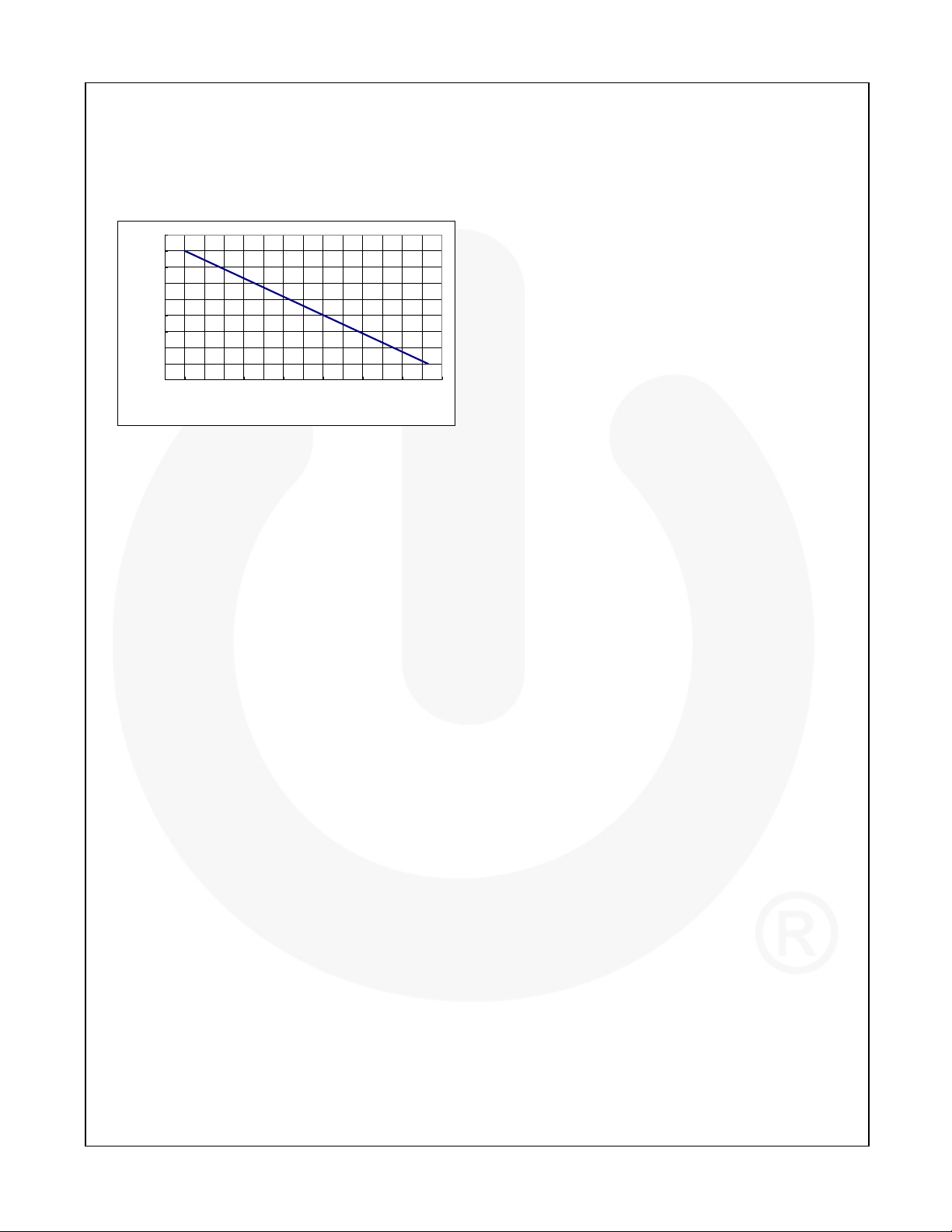
The HV pin can perform current limit to shrink the
tolerance of Over-Current Protection (OCP) under full
range of AC voltage, to linearly current limit curve, as
shown in Figure 25. FAN6754A also shrinks the V
level by half to lower the I
2
R
loss to increase the
SENSE
limit
heavy-load efficiency.
0.47
0.46
0.45
0.44
0.43
0.42
Vlimit (V)
0.41
0.4
0.39
0.38
100 120 140 1 60 180 200 220 240 260 280 300 320 340 360 380
DC Voltage on HV Pin (V)
Figure 25. Linearly Current Limit Curve
VDD Over-Voltage Protection (OVP)
VDD over-voltage protection prevents damage due to
abnormal conditions. If the V
voltage protection voltage (V
, the PWM pulses are disabled until VDD drops
VDDOVP
below the UVLO, then starts again. Over-voltage
conditions are usually caused by open feedback loops.
Sense-Pin Short-Circuit Protection
The FAN6754A provides safety protection for Limited
Power Source (LPS) tests. When the sense resistor is
shorted by soldering during production, the pulse-bypulse current limiting loses efficiency for the purpose of
providing over-power protection for the unit. The unit
may be damaged when the loading is larger than the
maximum load. To protect against a short circuit across
the current-sense resistor, the controller is designed to
immediately shut down if a continuously low voltage
(around 0.05V/120µs) on the SENSE pin is detected.
voltage is over the over-
DD
) and lasts for t
DD-OVP
D-
Thermal Protection
An NTC thermistor, R
be connected from the RT pin to ground. A constant
current, I
, is output from the RT pin. The voltage on
RT
the RT pin can be expressed as V
where I
is 100µA. At high ambient temperature, R
RT
is smaller, such that V
than 1.035V (V
(t
). If VRT is less than 0.7V (V
D-OTP1
off after 185µs (t
RTTH1
D-OTP2
NTC resistor for over-temperature protection,
connecting a series one 100KΩ resistor to ground to
prevent from noise interference is recommended. This
pin is limited by an internal clamping circuit.
, in series with resistor RA, can
NTC
• (R
RT=IRT
decreases. When VRT is less
RT
NTC
+ R
), the PWM turns off after 16ms
), the PWM turns
RTTH2
). If the RT pin is not connected to
Limited Power Control
The FB voltage increases every time the output of the
power supply is shorted or overloaded. If the FB voltage
remains higher than a built-in threshold for longer than
t
, PWM output is turned off. As PWM output is
D-OLP
turned off, V
begins decreasing.
DD
When VDD goes below the turn-off threshold (10V) the
controller is totally shut down and V
discharged to V
(6.5V) by I
DD-OLP
is continuously
DD
to lower the
DD-OLP
average input power. This is called two-level UVLO. V
is cycled again. This protection feature continues as
long as the overloading condition persists. This prevents
the power supply from overheating due to overloading
conditions.
Noise Immunity
Noise on the current sense or control signal may cause
significant pulse-width jitter, particularly in continuousconduction mode. Slope compensation helps alleviate
this problem. Good placement and layout practices
should be followed. Avoiding long PCB traces and
component leads, locating compensation and filter
components near the FAN6754A, and increasing the
power MOS gate resistance improve performance.
PTC
NTC
DD
),
© 2011 Fairchild Semiconductor Corporation www.fairchildsemi.com
FAN6754A • Rev. 1.0.3 12
Page 13
Physical Dimensions
8
5.00
4.80
3.81
A
FAN6754A — Highly Integrated Green-Mode PWM Controller
0.65
5
B
6.20
5.80
PIN ONE
INDICATOR
(0.33)
1.75 MAX
R0.10
R0.10
8°
0°
0.90
0.406
1
0.25
0.10
DETAIL A
SCALE: 2:1
4
1.27
0.51
0.33
0.50
0.25
SEATING PLANE
(1.04)
4.00
3.80
CMBA0.25
C
0.10 C
x 45°
GAGE PLANE
0.36
1.75
5.60
1.27
LAND PATTERN RECOMMENDATION
SEE DETAIL A
0.25
0.19
OPTION A - BEVEL EDGE
OPTION B - NO BEVEL EDGE
NOTES: UNLESS OTHERWISE SPECIFIED
A) THIS PACKAGE CONFORMS TO JEDEC
MS-012, VARIATION AA, ISSUE C,
B) ALL DIMENSIONS ARE IN MILLIMETERS.
C) DIMENSIONS DO NOT INCLUDE MOLD
FLASH OR BURRS.
D) LANDPATTERN STANDARD: SOIC127P600X175-8M.
E) DRAWING FILENAME: M08AREV13
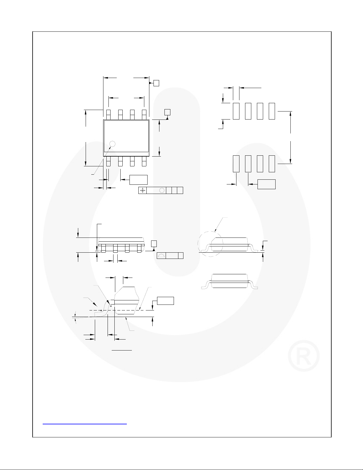
Figure 26. 8-Pin Small Outline Package (SOP) Package
Package drawings are provided as a service to customers considering Fairchild components. Drawings may change in any manner
without notice. Please note the revision and/or date on the drawing and contact a Fairchild Semiconductor representative to verify or
obtain the most recent revision. Package specifications do not expand the terms of Fairchild’s worldwide terms and conditions,
specifically the warranty therein, which covers Fairchild products.
Always visit Fairchild Semiconductor’s online packaging area for the most recent package drawings:
http://www.fairchildsemi.com/packaging/
© 2011 Fairchild Semiconductor Corporation www.fairchildsemi.com
FAN6754A • Rev. 1.0.3 13
.
Page 14
FAN6754A— Highly Integrated Green-Mode PWM Controller
© 2011 Fairchild Semiconductor Corporation www.fairchildsemi.com
FAN6754A • Rev. 1.0.3 14
 Loading...