

Page 1
May 2012
FAN6749
Highly Integrated Ultra Green-Mode PWM Controller
FAN6749 — Highly Integrated Ultra Green-Mode PWM Controller
Features
High-Voltage Startup
Low Operating Current: 1.8mA
Linearly Decreasing PWM Frequency to 24kHz
Proprietary Frequency Hopping to Reduce EMI
Two-Level Over-Current Protection (OCP),
1400ms Delay for Normal Peak Load
Two-Level OCP, 56ms Delay for Super Peak Load
Output Short-Circuit Protection (SCP)
Peak-Current Mode Operation with Cycle-by-Cycle
Current Limiting
HV Pin Brown-in/out Protection with Hysteresis
Constant Power Limit by HV Sampling
Internal FB Open-Loop Protection (OLP)
GATE Output Maximum Voltage Clamp: 14.5V
V
Over-Voltage Protection (OVP)
DD
Programmable Over-Temperature Protection (OTP)
Integrated 6ms Soft-Start Function
Internal Latch Circuit (OVP, OTP, OCP, OLP, SCP)
Internal OTP Sensor with Hysteresis
Applications
General-Purpose Switched-Mode Power Supplies and
Flyback Power Converters, including:
Power Adapters
Open-Frame SMPS; Specifically for SMPS with
Surge-Current Output, such as for Printer, Scanner,
Motor Drivers
Description
The FAN6749 highly integrated PWM controller
enhances the performance of flyback converters. To
minimize standby power consumption, a proprietary
Green-Mode function continuously decreases the
switching frequency under light-load conditions. Under
zero-load conditions, the power supply enters Burst
Mode and completely shuts off PWM output. Green
Mode helps power supplies meet international power
conservation requirements.
The FAN6749 is designed for SMPS with surge-current
output and incorporates a two-level Over-Current
Protection (OCP) function. Besides the cycle-by-cycle
current limiting, two-level OCP can handle peak loading
within a specified delay time.
FAN6749 also integrates a frequency-hopping function
that helps reduce EMI emission of a power supply with
minimum line filters. Built-in synchronized slope
compensation helps achieve stable peak-current control.
To keep constant output power limit over universal AC
input range, the current limit and OCP threshold voltage
are adjusted according to AC line voltage detected by
the HV pin. Gate output is clamped at 14.5V to protect
the external MOSFET from over-voltage damage.
Other protection functions include: AC input brownout
protection with hysteresis, Short-Circuit Protection
(SCP) for output-short condition, and V
Protection (OVP). For over-temperature protection, an
external NTC thermistor can be applied to sense the
ambient temperature. When OLP, OCP, SCP, V
or OTP is activated, an internal latch circuit latches off
the controller. The latch resets when V
OVP OCP OLP OTP SCP
Latch Latch Latch Latch Latch
There are three differences from FAN6748 to FAN6749:
Over-Voltage
DD
is removed.
DD
OVP,
DD
Over-current protection debounce time is extended
to 1400ms.
Brown-out debounce time is extended to 100ms.
No SENSE short-circuit protection function.
Ordering Information
Part Number Operating Temperature Range Package
FAN6749MLM -40 to +105°C 8-Pin Small Outline Package (SOP) Reel & Tape
© 2012 Fairchild Semiconductor Corporation www.fairchildsemi.com
FAN6749 • Rev. 1.0.1
Packing
Method
Page 2
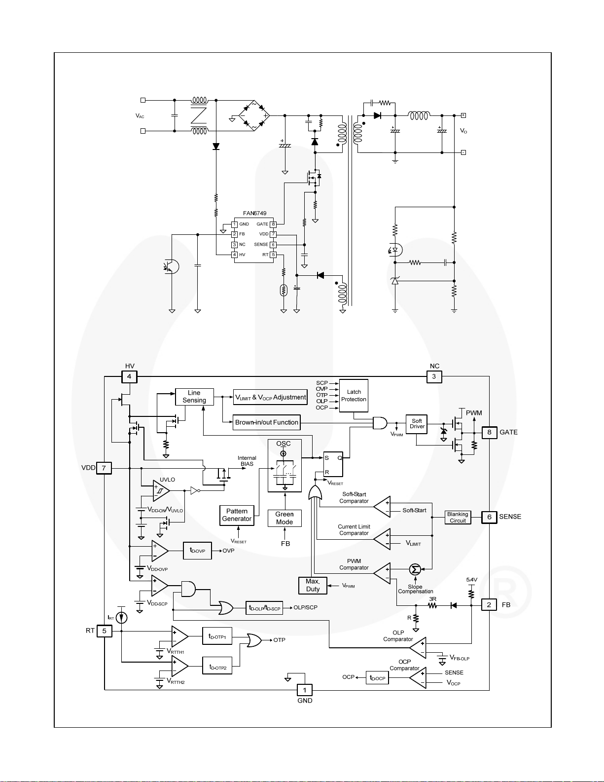
Application Diagram
FAN6749 — Highly Integrated Ultra Green-Mode PWM Controller
Figure 1. Typical Application
Internal Block Diagram
Figure 2. Functional Block Diagram
© 2012 Fairchild Semiconductor Corporation www.fairchildsemi.com
FAN6749 • Rev. 1.0.1 2
Page 3
Marking Information
Pin Configuration
ZXYTT
6749ML
TM
F - Fairchild Logo
Z - Plant Code
X - 1-Digit Year Code
Y - 1-Digit Week Code
TT - 2-Digit Die Run Code
T - Package Type (M=SOP)
M - Manufacture Flow Code
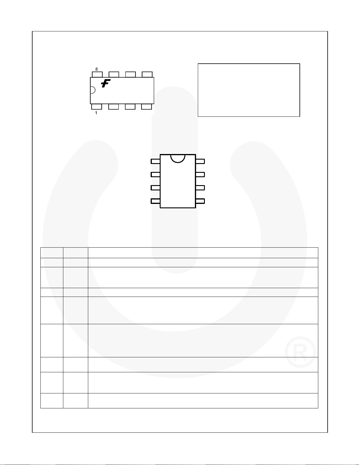
Figure 3. Top Mark
FAN6749 — Highly Integrated Ultra Green-Mode PWM Controller
Pin Definitions
Pin # Name Description
1 GND
2 FB
3 NC No Connection
4 HV
5 RT
6 SENSE
7 VDD
8 GATE
Ground Pin. A 0.1µF decoupling capacitor between VDD and GND is recommended.
Feedback Pin. The output voltage feedback information from the external compensation circuit is
fed into this pin. The PWM duty cycle is determined by comparing the FB signal with currentsense signal from the SENSE pin.
High-Voltage Startup. The HV pin is typically connected to the AC line input through an external
diode and a resistor (R
also to sense the line voltage. The line voltage information is used for brown-out protection and
power limit line compensation.
Over-Temperature Protection. An external NTC thermistor is connected from this pin to the
GND pin. Once the voltage of the RT pin drops below the threshold voltage, the controller latches
off the PWM. The RT pin also provides external latch protection. If the RT pin is not connected to
an NTC resistor for over-temperature protection, place a 100k resistor to ground to prevent
noise interference.
Current Sense. The sensed voltage is used for peak-current-mode control, over-current
protection, short-circuit protection, and cycle-by-cycle current limiting.
Power Supply of IC. A holdup capacitor typically connects from this pin to ground. A rectifier
diode in series with the transformer auxiliary winding connects to this pin to supply bias during
normal operation.
Gate Drive Output. The totem-pole output driver for the power MOSFET; internally limited to
V
GATE-CLAMP
.
GND
FB
NC
HV
Figure 4. Pin Configuration (Top View)
HV
18
2
3
7
6
54
). This pin is used not only to charge VDD capacitor during startup, but
GATE
VDD
SENSE
RT
© 2012 Fairchild Semiconductor Corporation www.fairchildsemi.com
FAN6749 • Rev. 1.0.1 3
Page 4
FAN6749 — Highly Integrated Ultra Green-Mode PWM Controller
Absolute Maximum Ratings
Stresses exceeding the absolute maximum ratings may damage the device. The device may not function or be
operable above the recommended operating conditions and stressing the parts to these levels is not recommended.
In addition, extended exposure to stresses above the recommended operating conditions may affect device reliability.
The absolute maximum ratings are stress ratings only.
Symbol Parameter Min. Max. Unit
VDD DC Supply Voltage
VFB FB Pin Input Voltage -0.3 7.0 V
V
SENSE Pin Input Voltage -0.3 7.0 V
SENSE
VRT RT Pin Input Voltage -0.3 7.0 V
VHV HV Pin Input Voltage 500 V
PD
JA
Power Dissipation (T
Thermal Resistance (Junction-to-Air) 150
TJ Operating Junction Temperature -40 +125
T
Storage Temperature Range -55 +150
STG
TL Lead Temperature (Wave Soldering or IR, 10 Seconds) +260
ESD
Human Body Model
Charged Device Model
Notes:
1. All voltage values, except differential voltages, are given with respect to the network ground terminal.
2. Stresses beyond those listed under “absolute maximum ratings” may cause permanent damage to the device.
3. ESD with the HV pin CDM=1000V and HBM=500V.
(1,2)
30 V
<50°C)
A
400 mW
C/W
C
C
C
(3)
, JEDEC:JESD22-A114 All Pins Except HV Pin 6 kV
(3)
, JEDEC:JESD22-C101 All Pins Except HV Pin 2 kV
Recommended Operating Conditions
The Recommended Operating Conditions table defines the conditions for actual device operation. Recommended
operating conditions are specified to ensure optimal performance to the datasheet specifications. Fairchild does not
recommend exceeding them or designing to Absolute Maximum Ratings.
Symbol Parameter Min. Typ. Max. Unit
RHV HV Startup Resistor 150 200 250 k
© 2012 Fairchild Semiconductor Corporation www.fairchildsemi.com
FAN6749 • Rev. 1.0.1 4
Page 5
Electrical Characteristics
VDD=15V and TA=25C unless otherwise noted.
Symbol Parameter Conditions Min. Typ. Max. Unit
VDD Section
VOP Continuously Operating Voltage Limited by VDD OVP 25 V
V
Threshold Voltage to Startup VDD Rising 16 17 18 V
DD-ON
V
DD-OFF
V
DD-OLP
V
UVLO
V
RESTART
V
DD-LH
V
DD-AC
V
DD-SCP
t
D-SCP
I
DD-ST
I
DD-OP1
I
DD-OP2
ILH
I
DD-OLP
V
DD-OVP
t
D-VDDOVP
Threshold Voltage to Stop
Switching in Protection Mode
Threshold Voltage to Turn On HV
Startup in Protection Mode
Threshold Voltage to Stop
Switching in Normal Mode
VDD Falling
VDD Falling 6.5 7.5 8.5 V
VDD Falling 6.0 6.5 7.0 V
Threshold Voltage to Enable HV
Startup to Charge VDD in Normal
VDD Falling 4.5 5.0 5.5 V
Mode
Threshold Voltage to Release
Latch Mode
VDD Falling 3.5 4.0 4.5 V
Threshold Voltage on VDD Pin for
Disable Brown-in to Avoid Startup
Failure
Threshold Voltage on VDD Pin for
Short-Circuit Protection (SCP)
Debounce Time for SCP
Startup Current V
Supply Current in PWM Operation
V
> V
FB
V
FB>VFB-OLP
& V
DD
DD-ON
=20V, VFB = 3V Gate
V
DD
FB-OLP
< V
DD-SCP
– 0.16V 30 µA
Open
Supply Current when PWM Stops VDD=15V, VFB < 1.4V 1.0 1.9 mA
Operating Current when V
in Protection Mode
OFF
Internal Sink Current
Threshold Voltage for V
Voltage Protection
Over-Voltage Protection
V
DD
Debounce Time
DD<VDD-
Over-
DD
VDD = 5V 100 120 140 µA
V
+0.1V
DD-OLP
28.5 29.0 29.9 V
160 200 240 µs
10 11 12
V
UVLO
+2.5
V
DD-OFF
+1.0
V
V
UVLO
+3 V
DD-OFF
+1.5
+3.5 V
UVLO
V
+2.0 V
DD-OFF
V
12 17 22 ms
1.8 2.4 mA
265 325 385 µA
FAN6749 — Highly Integrated Ultra Green-Mode PWM Controller
V
DD
V
DD-ON
GATE
V
UVLO
Normal Mode
V
RESTART
t
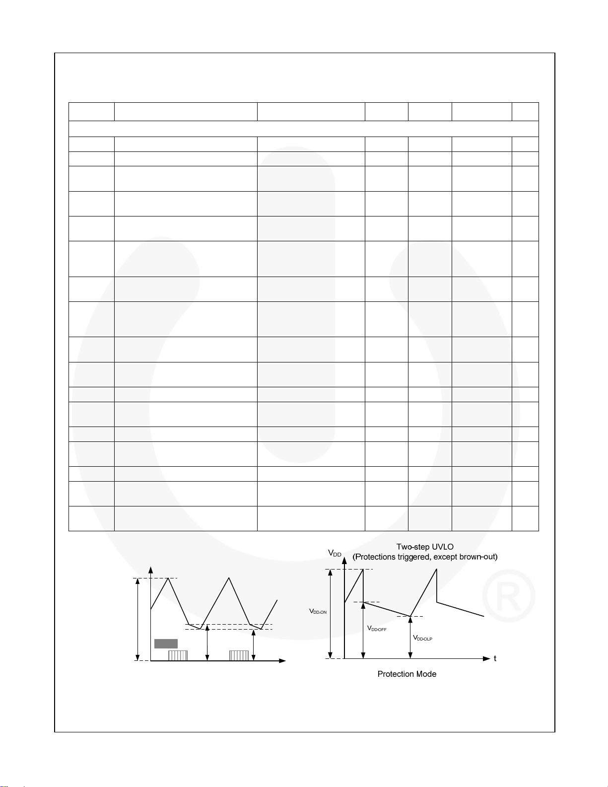
Figure 5. VDD Behavior
© 2012 Fairchild Semiconductor Corporation www.fairchildsemi.com
FAN6749 • Rev. 1.0.1 5
Continued on the following page…
Page 6
Electrical Characteristics (Continued)
VDD=15V and TA=25C unless otherwise noted.
FAN6749 — Highly Integrated Ultra Green-Mode PWM Controller
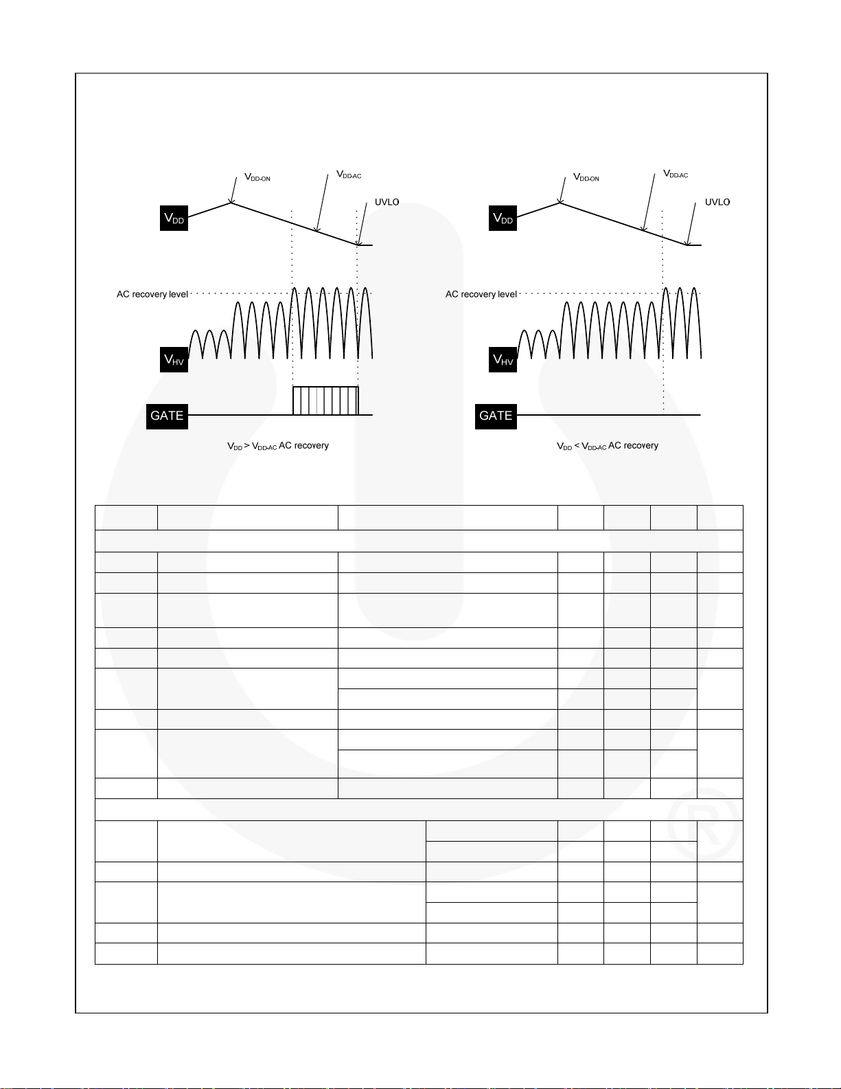
Figure 6. V
& AC Recovery
DD-AC
Symbol Parameter Conditions Min. Typ. Max. Unit
HV Section
IHV Supply Current from HV Pin VDC=120V, VDD=0V 2.0 3.5 5.0 mA
I
Leakage Current after Startup HV=500V, VDD=V
HV-LC
V
AC-OFF
V
AC-ON
△V
t
S-CYCLE
t
H-TIME
t
UPDATE
t
D-AC-OFF
Threshold Voltage for Brownout
DC Source Series R=200k to HV Pin
Threshold Voltage for Brown-In DC Source Series R=200k to HV Pin
V
AC
Line Voltage Sample Cycle
Line Voltage Hold Period
AC-ON
- V
DC Source Series R=200k to HV Pin
AC-OFF
(6)
Peak Line Voltage Data
Update Cycle for High / Low
Line Compensation
(6)
> V
V
FB
(6)
VFB < V
V
> V
FB
VFB = V
FB-N
FB-G
FB-N
FB-G
Debounce Time for Brown-out
+1V 1 20 µA
DD-OFF
90 100 110
100 110 120
8 10 17
170 200 230
400 520 640
18 23 28
V
V
V
µs
µs
20 24 28
64 72 80
70 100 130
ms
ms
Oscillator Section
f
Switching Frequency when VFB>V
OSC
t
Hopping Period 16 20 24 ms
HOP
f
Switching Frequency When VFB<V
OSC-G
FB-N
FB-G
Center Frequency
Hopping Range ±3.5 ±4.0 ±4.5
Center Frequency 20 24 28
Hopping Range ±1.25 ±1.55 ±1.85
fDV Frequency Variation vs. VDD Deviation VDD=11V to 22V 5 %
fDT Frequency Variation vs. Temperature Deviation
T
=-40 to 105C
A
62 65 68
kHz
kHz
5 %
Continued on the following page…
© 2012 Fairchild Semiconductor Corporation www.fairchildsemi.com
FAN6749 • Rev. 1.0.1 6
Page 7
FAN6749 — Highly Integrated Ultra Green-Mode PWM Controller
Electrical Characteristics (Continued)
VDD=15V and TA=25C unless otherwise noted.
Symbol Parameter Conditions Min. Typ. Max. Unit
Feedback Input Section
AV
ZFB FB Internal Pull-High Impedance 15 17 19 k
V
FB-OPEN
V
FB-OLP
t
D-OLP
V
V
SG Slope for Green-Mode Modulation 85 Hz/mV
V
FB-ZDCR
V
FB-ZDC
V
FB-ZDCR -
V
FB-ZDC
Input Voltage to Current-Sense
Attenuation
1/4.5 1/4.0 1/3.5 V/V
FB internal Biased Voltage FB Pin Open 5.2 5.4 5.6 V
Threshold Voltage for OLP 4.3 4.6 4.9 V
Debounce Time for OLP 40 56 72 ms
Threshold Voltage for Maximum
FB-N
Switching Frequency
Threshold Voltage for Minimum Switching
FB-G
Frequency
Threshold Voltage for Zero Duty Cycle
Recovery
Pin, FB Voltage(VFB=V
Pin, FB Voltage(VFB=V
) 2.5 2.7 2.9 V
FB-N
) 2.05 2.25 2.45 V
FB-G
1.9 2.1 2.3 V
Threshold Voltage for Zero Duty Cycle 1.8 2.0 2.2 V
Zero Duty Cycle Hysteresis 0.05 0.10 0.15 V
Current-Sense Section
tPD Delay to Output 65 200 ns
t
Leading-Edge Blanking 230 270 310 ns
LEB
V
LIMIT-L
V
LIMIT-H
V
V
OCP-L
OCP-H
Current Limit Level at Low Line
(V
Current Limit Level at High Line
(V
OCP Trigger Level at Low Line
(V
OCP Trigger Level at High Line
(V
AC-RMS
AC-RMS
AC-RMS
AC-RMS
= 86V)
= 259V)
=86V)
=259V)
tSS Soft-start time Startup Time 4.5 6.0 7.5 ms
t
Debounce Time for OCP V
D-OCP
PWM Frequency
=122V, Series R=200k
V
DC
to HV
=366V, Series R=200k
V
DC
to HV
=122V, Series R=200k
V
DC
to HV
=366V, Series R=200k
V
DC
to HV
SENSE>VOCP
1000 1400 1800 ms
0.790 0.825 0.860 V
0.690 0.725 0.760 V
0.45 0.48 0.51 V
0.39 0.42 0.45 V
Continued on the following page…
f
OSC
f
OSC-G
V
FB-ZDC
V
FB-ZDCR
V
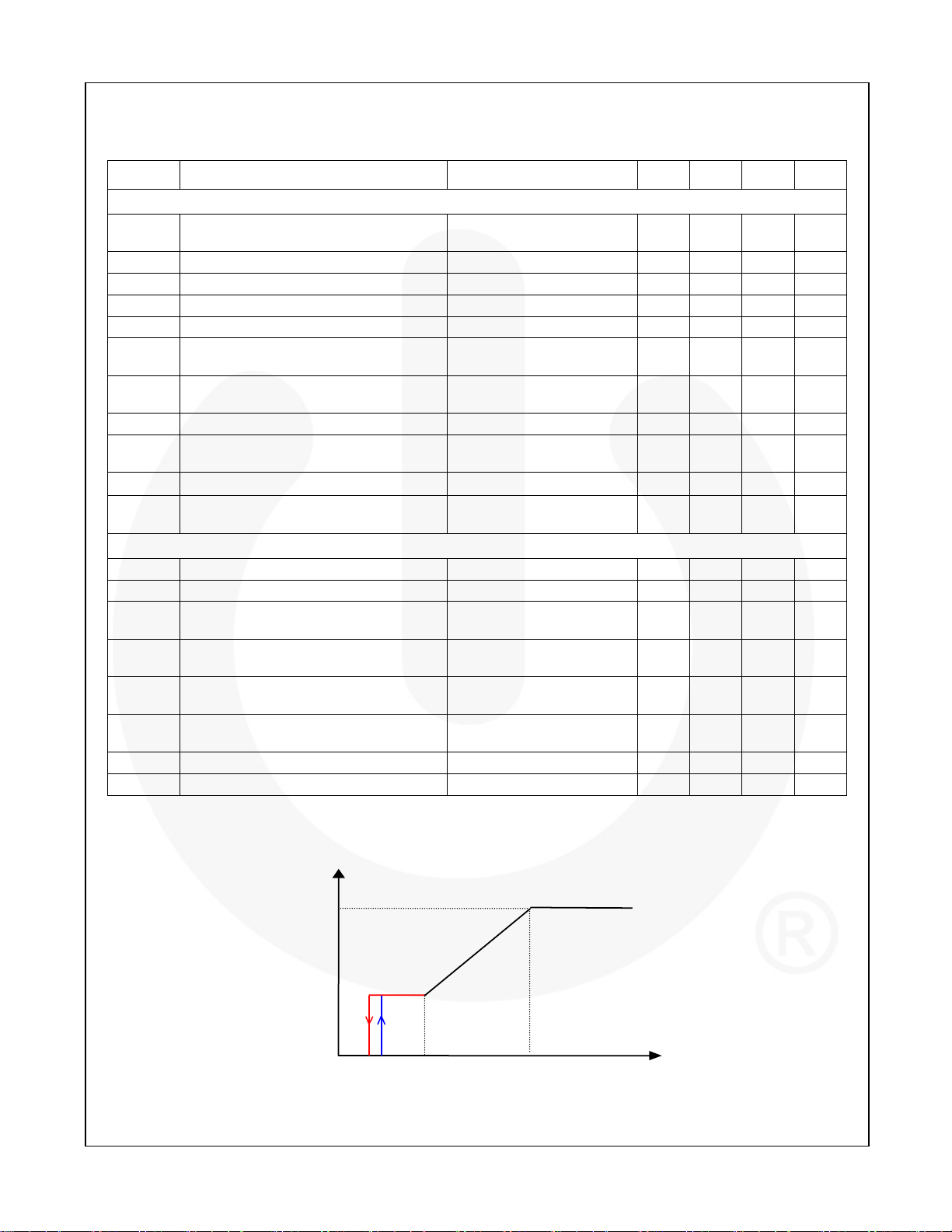
Figure 7. V
V
FB-G
vs. PWM Frequency
FB
FB-N
V
FB
© 2012 Fairchild Semiconductor Corporation www.fairchildsemi.com
FAN6749 • Rev. 1.0.1 7
Page 8

Electrical Characteristics (Continued)
VDD=15V and TA=25C unless otherwise noted.
Symbol Parameter Conditions Min. Typ. Max. Unit
GATE Section
D
Maximum Duty Cycle 80 85 90 %
MAX
V
Gate Low Voltage
GATE-L
V
Gate High Voltage
GATE-H
=15V, IO=50mA
V
DD
=12V, IO=50mA
V
DD
tr Gate Rising Time (20-80%) VDD=15V, CL=1nF 60 75 90
tf Gate Falling Time (80-20%) VDD=15V, CL=1nF 15 25 35
I
GATE-SINK
I
GATE-SOURCE
V
GATE-CLAMP
Gate Sink Current
Gate Sourcing Current
Gate Output Clamping Voltage VDD=22V 11.0 14.5 18.0
(6)
V
(6)
V
=15V 300
DD
=15V, GATE=6V 250
DD
RT Section
IRT Output Current of RT Pin 90 100 110 µA
V
RTTH1
V
RTTH2
R
t
D-OTP1
t
D-OTP2
Threshold Voltage for Over-Temperature
Protection
Threshold Voltage for Latch Triggering
Maximum External Resistance of RT Pin
OTP
to Trigger Latch Protection
Debounce Time for Over-Temperature
Protection Triggering
Debounce Time for Latch Triggering V
0.7V < V
< 1.05V, After
RT
14ms Latch Off
< 0.7V, After 165µs
V
RT
Latch Off
9.66 10.50 11.34 k
< V
V
RTTH2
< V
RT
< V
RT
90 165 240 µs
RTTH2
RTTH1
Over-Temperature Protection Section (OTP)
T
Protection Junction Temperature
OTP
T
Restart Junction Temperature
Restart
(4,6)
+135 °C
(5,6)
Notes:
4. When activated, the output is disabled and the latch is turned off.
5. The threshold temperature for enabling the output again and resetting the latch after OTP has been activated.
6. Guaranteed by design.
1.5 V
8 V
ns
ns
mA
mA
V
1.015 1.050 1.085 V
0.65 0.70 0.75 V
11 14 18 ms
-
T
OTP
25
°C
FAN6749 — Highly Integrated Ultra Green-Mode PWM Controller
© 2012 Fairchild Semiconductor Corporation www.fairchildsemi.com
FAN6749 • Rev. 1.0.1 8
Page 9

Typical Performance Characteristics
Figure 8. Startup Current (I
) vs. Temperature Figure 9. Operation Supply Current (I
DD-ST
DD-OP1
vs. Temperature
FAN6749 — Highly Integrated Ultra Green-Mode PWM Controller
)
Figure 10. Start Threshold Voltage (V
DD-ON
)
vs. Temperature
Figure 12. Supply Current Drawn from HV Pin (IHV)
vs. Temperature
Figure 11. Minimum Operating Voltage (V
DD-OFF
vs. Temperature
Figure 13. HV Pin Leakage Current After Startup (I
vs. Temperature
)
HV-LC
)
Figure 14. Frequency in Normal Mode (f
Temperature
© 2012 Fairchild Semiconductor Corporation www.fairchildsemi.com
FAN6749 • Rev. 1.0.1 9
OSC
) vs.
Figure 15. Maximum Duty Cycle (DCY
Temperature
MAX
) vs.
Page 10

Typical Performance Characteristics
FAN6749 — Highly Integrated Ultra Green-Mode PWM Controller
Figure 16. FB Open-Loop Trigger Level (V
Temperature
Figure 18. VDD Over-Voltage Protection (V
vs. Temperature
FB-OLP
DD-OVP
) vs.
)
Figure 17. Delay of FB Pin Open-Loop Protection (t
vs. Temperature
Figure 19. Output Current from RT Pin (IRT)
vs. Temperature
D-OLP
)
Figure 20. Over-Temperature Protection Threshold
Voltage (V
) vs. Temperature
RTTH1
Figure 21. Over-Temperature Protection Threshold
Voltage (V
) vs. Temperature
RTTH2
Figure 22. Brown-in (V
© 2012 Fairchild Semiconductor Corporation www.fairchildsemi.com
FAN6749 • Rev. 1.0.1 10
) vs. Temperature Figure 23. Brown-out (V
AC-ON
) vs. Temperature
AC-OFF
Page 11
A
Functional Description
Current Mode Control
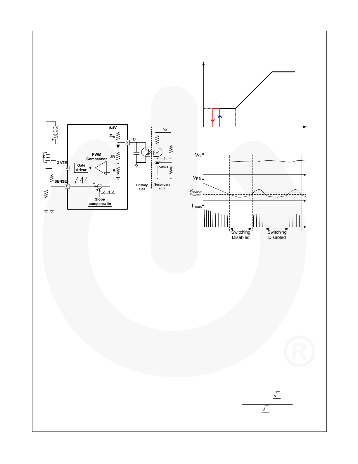
FAN6749 employs peak current mode control, as shown
in Figure 24. An opto-coupler (such as the H11A817A)
and a shunt regulator (such as the KA431) are typically
used to implement the feedback network. Comparing the
feedback voltage with the voltage across the R
resistor makes it possible to control the switching duty
cycle. The built-in slope compensation stabilizes the
current loop and prevents sub-harmonic oscillation.
sense
FAN6749 — Highly Integrated Ultra Green-Mode PWM Controller
f
S
f
OSC
f
OSC-G
Figure 24. Current Mode Control Circuit Diagram
Green-Mode Operation
FAN6749 modulates the PWM frequency as a function
of the FB voltage to improve the medium- and light-load
efficiency, as shown in Figure 25. Since the output
power is proportional to the FB voltage in current mode
control, the switching frequency decreases as load
decreases. In heavy-load conditions, the switching
frequency is fixed at 65kHz. Once V
V
(2.7V), the PWM frequency starts linearly
FB-N
decreasing from 65kHz to 24kHz to reduce switching
losses. As V
drops to V
FB
(2.25V), where switching
FB-G
frequency is decreased to 24kHz, the switching frequency
is fixed to avoid acoustic noise.
When V
falls below V
FB
(2.0V) as load decreases
FB-ZDC
further, FAN6749 enters Burst Mode, where PWM
switching is disabled. Then the output voltage starts to
drop, causing the feedback voltage to rise. Once V
rises above V
(2.1V), switching resumes. Burst
FB-ZDCR
Mode alternately enables and disables switching,
thereby reducing switching loss for lower power
consumption, as shown in Figure 26
decreases below
FB
FB
V
FB-ZDCVFB-ZDCRVFB-G
V
FB-N
V
FB
Figure 25. VFB vs. PWM Frequency
Figure 26. Burst Switching in Green Mode
Operating Current
In normal condition, operating current is around 1.8mA
(I
); when VFB<1.4V, operating current is further
DD-OP1
reduced to 1mA (I
) by disabling several blocks of
DD-OP2
FAN6749. The low operating current improves light-load
efficiency and reduces the requirement of V
hold-up
DD
capacitance.
High-Voltage Startup and Line Sensing
The HV pin is typically connected to the AC line input
through an external diode and a resistor (R
in Figure 27. When AC line voltage is applied, the V
hold-up capacitor is charged by the line voltage through
the diodes and resistor. After V
turn-on threshold voltage (V
charging V
capacitor is switched off and VDD is
DD
voltage reaches the
DD
), the startup circuit
DD-ON
supplied by the auxiliary winding of the transformer.
Once FAN6749 starts up, it continues operation until
V
drops below 6.5V (V
DD
). The IC startup time with a
UVLO
given AC line input voltage is given as:
), as shown
HV
DD
2
V
tRC
STARTUP HV DD
ln
VV
CIN DDON
AC IN
2
(1)
© 2012 Fairchild Semiconductor Corporation www.fairchildsemi.com
FAN6749 • Rev. 1.0.1 11
Page 12
V
R
R
FAN6749 — Highly Integrated Ultra Green-Mode PWM Controller
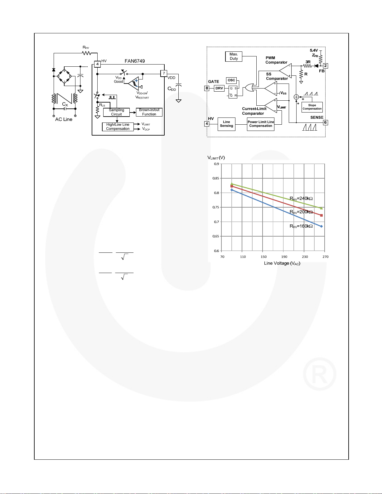
Figure 27. Startup Circuit
The HV pin detects the AC line voltage using a switched
voltage divider that consists of external resistor (R
and internal resistor (R
), as shown in Figure 27. The
LS
HV
)
internal line-sensing circuit detects line voltage using a
sampling circuit and a peak-detection circuit. Since the
voltage divider causes power consumption when it is
switched on, the switching is driven by a signal with a
very narrow pulse width to minimize power loss. The
sampling frequency is adaptively changed according to
the load condition to minimize the power consumption in
the light-load condition.
Based on the detected line voltage, brown-in and brownout thresholds are determined as:
ONAC
IN-BROWN
OUT-BROWN
(RMS)
(RMS)
HV
200k
HV
200k
2
V
OFFAC
2
(2)
(3)
Since the internal resistor (RLS=1.62k) of the voltage
divider is much smaller than R
given as s function of R
HV
.
Note that VDD must be larger than V
, the thresholds are
HV
to start up,
DD-AC
even though sensed line voltage satisfies Equation 2.
High/Low Line Compensation for Constant
Power Limit
FAN6749 has cycle-by-cycle current limit, as shown in
Figure 28, which limits the maximum input power with a
given input voltage. If the output consumes beyond this
maximum power, the dropping output voltage triggers
the overload protection.
As shown in Figure 28, the high/low line compensation
block adjusts the current limit level, V
line voltage. Figure 29 shows how the cycle-by-cycle
current-limit level changes with the line voltage for
different R
resistors. To maintain the constant output
HV
power limit regardless of line voltage, the cycle-by-cycle
current limit level, V
, decreases as line voltage
LIMIT
increases. The current-limit level is also proportional to
the R
resistor value and power limit level can be tuned
HV
using different R
resistors.
HV
, based on the
LIMIT
Figure 28. Cycle-by-Cycle Current-Limit Circuit
Figure 29. Current Limit vs. Line Voltage
Two-Level Over-Current Protection (OCP)
Other than cycle-by-cycle current limiting, FAN6749
applies another threshold voltage, V
sense. As shown in Figure 28, when peak of V
exceeds V
at each pulse for a period of time, t
OCP
over-current protection (OCP) is triggered. This
protection is designed for applications with surge-current
outputs. If a peak load is present for less than t
controller operates as usual. If the peak load continues
longer than t
, GATE output is stopped to protect the
D-OCP
converter from overload condition.
Like V
LIMIT
, the V
is adjusted by high/low line
OCP
compensation block to maintain a constant over-current
protection level, regardless of line voltage. Figure 31
shows how V
different R
HV
changes with the line voltage with
OCP
resistors.
When OCP is triggered, it is recommended to have
V
FB>VFB-N
for whole AC input range. VFB>V
switching frequency is fixed at 65kHz. If OCP is
triggered in the frequency-reduction region (V
output current is reduced due to lower switching
frequency. It causes the difference of OCP-triggering
point between high and low AC input voltages.
, for current
OCP
D-OCP
ensures
FB-N
FB<VFB-N
SENSE
D-OCP
, the
;
),
© 2012 Fairchild Semiconductor Corporation www.fairchildsemi.com
FAN6749 • Rev. 1.0.1 12
Page 13
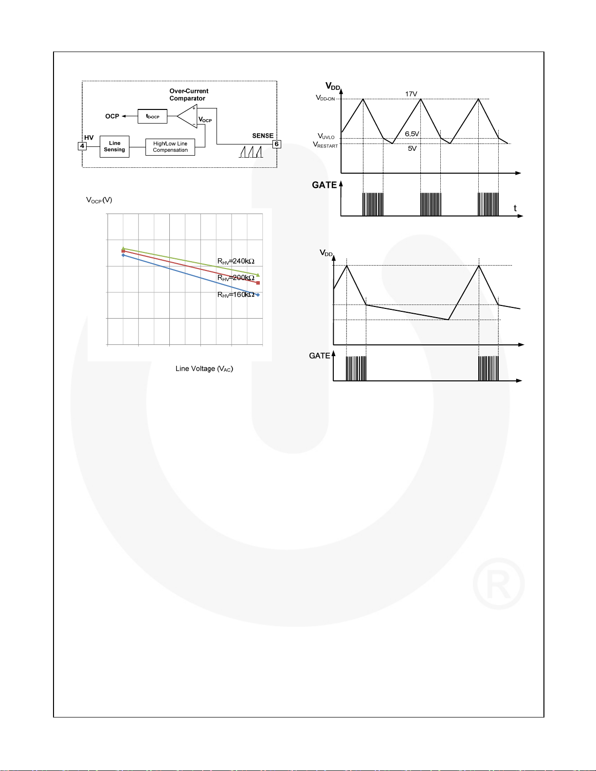
Figure 30. Over-Current Protection Circuit
FAN6749 — Highly Integrated Ultra Green-Mode PWM Controller
0.55
0.5
0.45
0.4
0.35
0.3
70 110 150 190 230 270
Figure 31. V
vs. Line Voltage
OCP
Short Circuit Protection (SCP)
The VDD voltage decreases every time the output of the
power supply is shorted because the impedance at
secondary windings becomes far lower than at auxiliary
winding and currents choose the low-impedance path.
When V
t
D-SCP
is larger than V
FB
; if V
DD
is lower than V
FB-OLP
over a debounce time of
, PWM output is
DD-SCP
latched off.
Under-Voltage Lockout (UVLO)
As shown in Figure 32, as long as protection is not
triggered, the turn-off threshold of V
at V
(6.5V). When a protection is triggered, the VDD
UVLO
level to terminate PWM gate switching is changed to
V
(11V), as shown in Figure 33. When VDD drops
DD-OFF
below V
operating current from V
down the discharge of V
, the switching is terminated and the
DD-OFF
is reduced to I
DD
until VDD reaches V
DD
This delays restart after shutdown by protection to
minimize the input power and voltage/current stress of
switching devices during fault condition.
is fixed internally
DD
, to slow
DD-OLP
DD-OLP
.
Figure 32. VDD UVLO in Normal Mode
V
DD-ON
V
DD-OFF
V
DD-OLP
17V
11V
7.5V
t
Figure 33. VDD UVLO in Protection Mode
Leading-Edge Blanking (LEB)
Each time the power MOSFET is switched on, a turn-on
spike occurs on the sense resistor. To avoid premature
termination of the switching pulse, a leading-edge
blanking time, t
, is introduced. During this blanking
LEB
period, the current-limit comparator is disabled and
cannot switch off the gate driver.
Gate Output / Soft Driving
The BiCMOS output stage has a fast totem-pole gate
driver. The output driver is clamped by an internal 14.5V
Zener diode to protect power MOSFET gate from over
voltage. A soft driving is implemented to minimize
electromagnetic interference (EMI) by reducing the
switching noise.
VDD Over-voltage Protection (OVP)
VDD over-voltage protection prevents IC damage from
over-voltage exceeding the IC voltage rating. When the
V
voltage exceeds 29V, the protection is triggered.
DD
This protection is typically caused by an open circuit in
the secondary-side feedback network.
© 2012 Fairchild Semiconductor Corporation www.fairchildsemi.com
FAN6749 • Rev. 1.0.1 13
Page 14
RRI
Soft-Start
FAN6749 has an internal soft-start circuit that
progressively increases the cycle-by-cycle current limit
level of the MOSFET for 6ms during startup to establish
the correct working conditions for transformers and
capacitors to operate.
Over-Temperature Protection (OTP)
The RT pin provides adjustable Over-Temperature
Protection (OTP) and an external latch-triggering
function. For OTP application, an NTC thermistor, R
usually in series with a resistor, R
, is connected
A
between the RT pin and ground. The internal current
source, I
At high ambient temperature, R
reduces V
longer than t
, (100µA) introduces voltage on RT as:
RT
)(
ANTCRTRT
decreases, which
. When VRT is lower than V
RT
(14ms), the protection is triggered
D-OTP1
NTC
RTTH1
(1.050V) for
and FAN6749 enters Latch Mode protection.
NTC
(4)
,
The OTP can be also trigged by pulling down the RT pin
voltage using an opto-coupler or transistor. Once V
less than V
(0.7V) for longer than t
RTTH2
D-OTP2
is
RT
(165µs),
the protection is triggered and FAN6749 enters Latch
Mode protection.
When V
falls below 1.9V, the RT pin function is
FB
disabled for lower power consumption. If OTP is not
used, place a 100k resistor between this pin and
ground to prevent noise interference.
Noise Immunity
Noise on the current sense or control signal may cause
significant pulse-width jitter, particularly in continuousconduction mode. Slope compensation helps alleviate
this problem. Good placement and layout practices
should be followed. Avoiding long PCB traces and
component leads, locating compensation and filter
components near the FAN6749, and increasing the
power MOS gate resistance improve performance.
FAN6749 — Highly Integrated Ultra Green-Mode PWM Controller
© 2012 Fairchild Semiconductor Corporation www.fairchildsemi.com
FAN6749 • Rev. 1.0.1 14
Page 15
Physical Dimensions
8
5.00
4.80
3.81
FAN6749 — Highly Integrated Ultra Green-Mode PWM Controller
A
0.65
5
B
6.20
5.80
PIN ONE
INDICATOR
(0.33)
1.75 MAX
R0.10
R0.10
8°
0°
0.90
0.406
1
0.25
0.10
DETAIL A
SCALE: 2:1
4
1.27
0.51
0.33
0.50
0.25
SEATING PLANE
(1.04)
4.00
3.80
C
x 45°
GAGE PLANE
0.36
1.75
5.60
1.27
CMBA0.25
LAND PATTERN RECOMMENDATION
SEE DETAIL A
0.25
0.19
0.10 C
OPTION A - BEVEL EDGE
OPTION B - NO BEVEL EDGE
NOTES: UNLESS OTHERWISE SPECIFIED
A) THIS PACKAGE CONFORMS TO JEDEC
MS-012, VARIATION AA, ISSUE C,
B) ALL DIMENSIONS ARE IN MILLIMETERS.
C) DIMENSIONS DO NOT INCLUDE MOLD
FLASH OR BURRS.
D) LANDPATTERN STANDARD: SOIC127P600X175-8M.
E) DRAWING FILENAME: M08AREV13
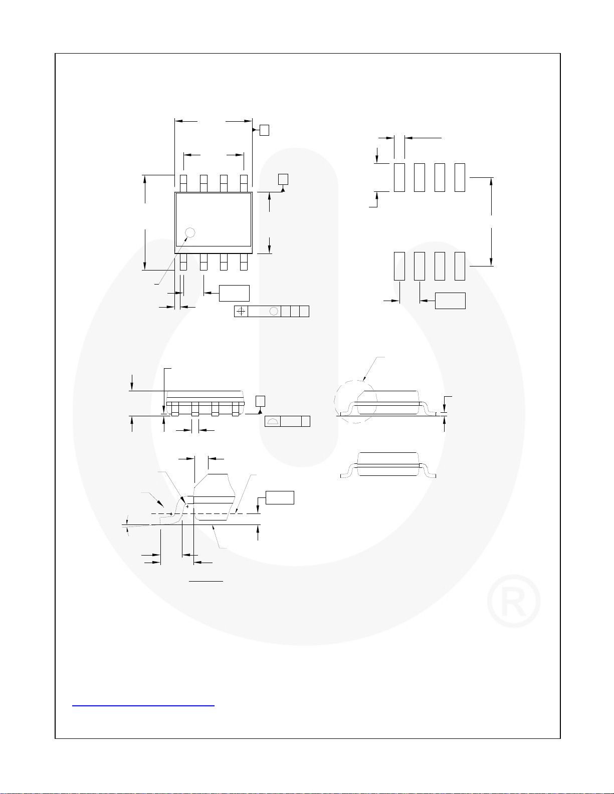
Figure 34. 8-Pin SOP-8 Package
Package drawings are provided as a service to customers considering Fairchild components. Drawings may change in any manner
without notice. Please note the revision and/or date on the drawing and contact a Fairchild Semiconductor representative to verify or
obtain the most recent revision. Package specifications do not expand the terms of Fairchild’s worldwide terms and conditions,
specifically the warranty therein, which covers Fairchild products.
Always visit Fairchild Semiconductor’s online packaging area for the most recent package drawings:
http://www.fairchildsemi.com/packaging/
.
© 2012 Fairchild Semiconductor Corporation www.fairchildsemi.com
FAN6749 • Rev. 1.0.1 15
Page 16
FAN6749 — Highly Integrated Ultra Green-Mode PWM Controller
© 2012 Fairchild Semiconductor Corporation www.fairchildsemi.com
FAN6749 • Rev. 1.0.1 16
 Loading...