

Page 1
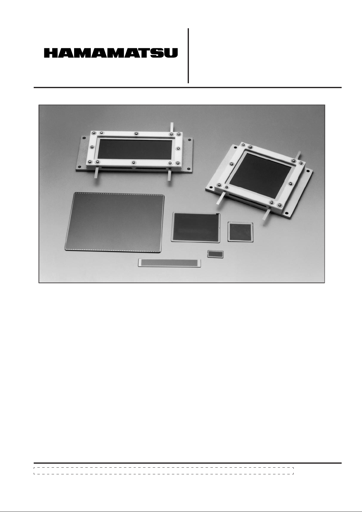
A microchannel plate (MCP) is a secondary electron multiplier
consisting of an array of glass capillaries (channels) fused into
the form of a thin plate. Each channel has an internal diameter
of 6 µm to 25 µm and works as an independent electron
multiplier, making possible the detection and amplification of
two-dimensional information.
In addition to previously available circular-type MCPs,
Hamamatsu has available seven types of rectangular MCPs. Of
these, three standard types include demountable assemblies
which have electrode leads and read-out devices. Using these,
it is possible to alleviate dimensional limitations encountered
when building the MCPs into instruments as compared with
circular types, greatly facilitating the effective use of these
devices. The demountable assembly can be selected as combinations of MCPs (1 to 3 stage) and a read-out device (singleanode, multi-anode or phosphor screen). Making possible the
selection of the most suitable configuration for your application,
while facilitating replacement as well.
Subject to local technical requirements and regulations, availability of products included in this promotional material may vary. Please consult with our sales office.
Information furnished by HAMAMATSU is believed to be reliable. However, no responsibility is assumed for possible inaccuracies or omissions.
Specifications are subjected to change without notice. No patent rights are granted to any of the circuits described herein. © 1999 Hamamatsu Photonics K. K.
RECTANGULAR MCP AND
ASSEMBLY SERIES
FEATURES
• Convenience of use due to fewer leads
• Choice and interchangeability of MCP and read-out
devices
• High gain and low noise
• Two-dimensional image intensification
• Fast time response
• Immunity to magnetic fields
• Sensitive to electrons, ions, VUV lights, X-rays and
γ-rays
• Stable in air
• Low power consumption
• Small size and light weight
• Can be baked in vacuum at up to 350°C
APPLICATIONS
Detection and imaging of electrons, ions,
VUV lights, X-rays and γ-rays
• Mass spectroscopy
• Energy spectroscopy
• High-speed response CRTs
Page 2
RECTANGULAR MCP AND ASSEMBLY SERIES
MCP
ASSEMBLY MOUNTING SCREW M2 (4 pcs.)
INSULATOR SUPPORT SCREW M2 (4 TO 6 pcs.)
READ-OUT DEVICE
SUBSTRATE
MCP DIMENSIONAL OUTLINES (Unit: mm)
C
B
A
INPUT SIDE OUTPUT SIDE
C’
B’
A’
D
EFFECTIVE AREA
ELECTRODE
INDICATOR
θ
A
Type
Parameters
F6492 F2370-01 F4772-01 F2806-01 F1943-02 F2805-03 F2396-04 Unit
Outer dimensions A × A’ 139.9 × 8.9 15.9 × 9.4 61.9 × 13.9 49.9 × 39.9 87.9 × 37.9 59.9 × 59.9 96.9 × 78.9 mm
Electrode dimensions B × B’ 138 × 8 15 × 8.5 61 × 9.4 49 × 39 87 × 37 58 × 58 95.6 × 77.3 mm
MCP Effective dimensions C × C’
127 × 4 13 × 6.5 55 × 8 45 × 35 81 × 31 53 × 53 90 × 72 mm
Thickness D 0.48 0.60 0.80 1.00 mm
Channel diameter 12 15 20 25
µ
m
Channel pitch 15 19 25 31
µ
m
Bias angle θ 8 degrees
Open area ratio 60 %
Electrode material Inconel –
ELECTRICAL CHARACTERISTICS
(Supply Voltage: 1000 V, Vacuum: 1.3 × 10
-4
Pa (1 × 10⁻⁶ Torr), Ambient Temperature: 25 °C)
Current Gain More than 10
4 —
Plate Resistance 10 to 100 100 to 500 20 to 200 20 to 120 10 to 50 MΩ
Dark Current Less than 5 × 10
-13
A/cm
2
Max. Linear Output Signal Up to 7% of the strip current
B
–
MAXIMUM RATINGS
Supply Voltage
C
1000 1100 1200 V
Ambient Temperature –50 to + 70 –50 to +50 °C
A This indicator shows the MCP input side and the direction of channel bias.
The F2806-01 has bias angle of opposite direction against the perpendicular line shown in the figure.
B The strip current is the current which flows along the channel wall when a voltage is supplied between the MCP input and output and is given
by Supply voltage/Plate resistance.
C At a vacuum of 1.3 × 10
-4
Pa (1 × 10⁻⁶ Torr) or less.
Comment: Consult us for other dimensions, details on MCP resistance ranges and other information.
TMCPA0028EB
Page 3

MCP
ASSEMBLY MOUNTING SCREW M2 (4 pcs.)
INSULATOR SUPPORT SCREW M2 (4 TO 6 pcs.)
READ-OUT DEVICE
SUBSTRATE
ASSEMBLY DIMENSIONS (Unit: mm)
ASSEMBLY DIMENSIONS TABLE
Symbol Description F2813 F2814 F3490 Unit
A × C’ Assembly outer dimensions 128 × 54 96 × 76 78 × 29.5 mm
B × D’ Mounting screw hole pitch 120 × 46 86 × 68 72 × 18 mm
C × C’ Insulator outer dimensions 104 × 54 76 × 76 66 × 29.5 mm
D × D’ Insulator support screw pitch 96 × 46 68 × 68 56 × 24 mm
E × E’ MCP effective dimensions 81 × 31 53 × 53 55 × 8mm
F × D’ Assembly screw spacing 79 × 46 51 × 68 56 × 24 mm
H × H’ Effective dimensions of readout device 80 × 30 50 × 50 52 × 7mm
Distance from No. 1 10.9 10.9
G bottom of substrate of 2 11.9 11.9 11.9 mm
to insulator surface MCP 3 11.9 12.9
Distance from MCP No. 1 2.7 2.5 3.8
J input surface to of 2 3.1 2.7 3.3 mm
insulator surface MCP 3 2.5 2.9 2.9
TMCPA0029EB
F
E
D
C
B
A
E’
D’
C’
H
G
H’
3
J
3
20
LEAD (SUS)
MCP
READ-OUT DEVICE
SCREW M2 (SUS)
INSULATOR (Al2O3)
SUBSTRATE
(SUS)
DEGASSING SPACE
4- 3.5
Page 4

MCP
ASSEMBLY MOUNTING SCREW M2 (4 pcs.)
INSULATOR SUPPORT SCREW M2 (4 TO 6 pcs.)
READ-OUT DEVICE
SUBSTRATE
ASSEMBLY EXPLODED VIEW
GENERAL
MCP
Unit
Parameter
Single-Stage Two-Stage Three-Stage
Channel Diameter F3490 type: 12, F2813 type: 15, F2814 type: 20 µm
Read-Out Device
Without read-out device, with single anode, multianode or phosphor screen (P-11, P-20, P-47)
A
–
A The phosphor screen read-out type is not available for non-demountable type or three-stage series.
ELECTRICAL CHARACTERISTICS
(Supply Voltage: 1000 V per stage, Vacuum: In the order of 1.3 × 10
-5
Pa (10-7 Torr) , Ambient Temperature: 25 °C)
Current Gain 10
4
10
6
107 to 10
8
–
Dark Noise Less than 5 × 10
-13
A/cm2Less than 3 s-1/cm2 (cps/cm2) BLess than 3 s-1/cm2 (cps/cm2)
B
–
Pulse Height Resolution — Less than 120 Less than 80 %
Max. Linear Output Signal Up to 7% of the strip current –
B Dark noise lower than the valley of pulse height distribution for the signal is not taken into account.
MAXIMUM RATINGS
CC
CC
C
MCP Supply Voltage 1000 2000 3000 V
MCP-Out—Anode Voltage 1000 V
MCP-Out—Phosphor Screen Voltage 4000 V
Substrate—Other Terminals Voltage 6000 V
Baking Temperature 350 °C
C At a vacuum of 1.3 × 10⁻⁵ Pa (1 × 10⁻⁷ Torr) and an ambient temperature of 25 °C.
The phosphor screen read-out type assemblies should be operated in a vacuum below 2.6 × 10⁻⁵ Pa (2 × 10⁻⁷ Torr).
PHOSPHOR SCREEN EMISSION CHARACTERISTICS
Phosphor type
P-11 P-20 P-47 Unit
Parameter
Wavelength at Peak Emission 450 530 to 560 410 nm
Decay Time <10%> 460 50 to 2000 0.08 µs
TMCPC0029EA
Page 5

RECTANGULAR MCP AND ASSEMBLY SERIES
CHANNEL WALL
STRIP CURRENT
PRIMARY
ELECTRON
OUTPUT
ELECTRON
V
D
HAMAMATSU PHOTONICS K.K., Electron Tube Center
314-5, Shimokanzo, Toyooka-village, Iwata-gun, Shizuoka-ken, 438-0193, Japan, Telephone: (81)539/62-5248, Fax: (81)539/62-2205
U.S.A.:
Hamamatsu Corporation: 360 Foothill Road, Bridgewater, N.J. 08807-0910, U.S.A., Telephone: (1)908-231-0960, Fax: (1)908-231-1218
Germany:
France:
United Kingdom:
North Europe:
Italy:
Hamamatsu Photonics Italia S.R.L.: Strada della Moia, 1/E 20020 Arese (Milano), Italy, Telephone: (39)02-935 81 733, Fax: (39)02-935 81 741
ORDERING INFORMATION (Type No. Designation)
WIRING EXAMPLES
■ SPECIAL MCPs AND ASSEMBLIES
• Hamamatsu Photonics can receive orders for special MCPs and assemblies not included in the standard product line.
• Feel free to consult us on MCPs with an aperture (for use with reflecting electron microscopes), CsI deposition (for higher
• For multianode types, specify the desired anode pattern.
• Assemblies with a phosphor-coated fiber plate are available to enable fiber coupling to solid state imaging devices (CCD
• Assemblies mounted on custom vacuum flanges or substrates are also available.
OPERATING PRINCIPLE
As shown in the figure, when a voltage VD is supplied across the
input-side and output-side electrodes of the MCP, a potential
gradient is built up along the channel direction. If an incident
electron strikes an inner wall on the input side, a number of
secondary electrons are emitted. These secondary electrons
are accelerated by the potential gradient and travel along a
parabolic path determined by the initial velocity. They then
collide with the opposing wall surface, causing secondary
electrons to be emitted again. In this manner, the electrons
collide repeatedly within the channel as they pass towards the
output side. The result is a logarithmic multiplication of the
electron current appearing at the output.
CURRENT GAIN AND LIFE CHARACTERISTICS
• Current Gain vs. Supply Voltage
10
5
10
4
10
3
10
2
600 800 1000 1200
SUPPLY VOLTAGE (V)
CURRENT GAIN
TMCPB0029EA
■ PRECAUTIONS FOR USE
• Don’t touch the MCP and assembly parts with bare hands.
• Always handle the MCP in an area that is maintained at the same level of cleanliness as a clean room since dust and
humidity may adversely affect MCP characteristics.
• The MCP should be kept in vacuum or nitrogen atmosphere when storing it after delivery.
• If excessive outgas from the MCP occurs, perform vacuum-baking of the MCP at +350°C maximum in an evacuating
system. Alternatively, electron bombarding of the MCP is effective. (Please consult our sales office for details.)
• The MCP and MCP assemblies must be operated in a vacuum below 1.3 × 10
-3
Pa (1 × 10⁻⁵ Torr). However, phosphor
output MCP assemblies and other assemblies using a three-stage MCP should be operated in a vacuum below
1.3 × 10
-4
Pa (1 × 10⁻⁶ Torr).
• MCP Configuration
• Life
RELATIVE OUTPUT
ACCUMULATED CHARGE OF OUTPUT SIGNAL (C/cm2)
10
–4
10
–3
10
–2
10
–1
1.0
0.5
0
SUPPLY VOLTAGE : 1000 V
OUTPUT CURRENT DENSITY : 50 nA/ 15 mm
TMCPB0030EC
TMCPC0030EA
Page 6

RECTANGULAR MCP AND ASSEMBLY SERIES
HAMAMATSU PHOTONICS K.K., Electron Tube Center
314-5, Shimokanzo, Toyooka-village, Iwata-gun, Shizuoka-ken, 438-0193, Japan, Telephone: (81)539/62-5248, Fax: (81)539/62-2205
U.S.A.:
Hamamatsu Corporation: 360 Foothill Road, Bridgewater, N.J. 08807-0910, U.S.A., Telephone: (1)908-231-0960, Fax: (1)908-231-1218
Germany:
Hamamatsu Photonics Deutschland GmbH: Arzbergerstr. 10, D-82211 Herrsching am Ammersee, Germany, Telephone: (49)8152-375-0, Fax: (49)8152-2658
France:
Hamamatsu Photonics France S.A.R.L.: 8, Rue du Saule Trapu, Parc du Moulin de Massy, 91882 Massy Cedex, France, Telephone: (33)1 69 53 71 00, Fax: (33)1 69 53 71 10
United Kingdom:
Hamamatsu Photonics UK Limited: Lough Point, 2 Gladbeck Way, Windmill Hill, Enfield, Middlesex EN2 7JA, United Kingdom, Telephone: (44)20-8-367-3560, Fax: (44)20-8-367-6384
North Europe:
Hamamatsu Photonics Norden AB: Smidesvägen 12, SE-171-41 Solna, Sweden, Telephone: (46)8-509-031-00, Fax: (46)8-509-031-01
Italy:
Hamamatsu Photonics Italia S.R.L.: Strada della Moia, 1/E 20020 Arese (Milano), Italy, Telephone: (39)02-935 81 733, Fax: (39)02-935 81 741
ORDERING INFORMATION (Type No. Designation)
F 2 8 1 3 - 2 2 S
Third suffix : readout device
No suffix : without read-out device
S : Single anode
M: Multianode
P : Phosphor screen
(select P-11, 20 or 47)
Second suffix : Channel diameter
Assembly type 1 : 12 µm (F3490 type)
2 : 15 µm (F2813 type)
3 : 20 µm (F2814 type)
First suffix : Number of MCPs
1 : Single-stage
2 : Two-stage
3 : Three-stage
Note: In ordering the MCP only, specify only the type No. of MCP.
WIRING EXAMPLES
■ SPECIAL MCPs AND ASSEMBLIES
• Hamamatsu Photonics can receive orders for special MCPs and assemblies not included in the standard product line.
Please specify the shape, effective dimensions, thickness and other parameters you need.
• Feel free to consult us on MCPs with an aperture (for use with reflecting electron microscopes), CsI deposition (for higher
quantum efficiency in the VUV to X-ray range), aluminum film coating (as a barrier to ions or radiation), MgO coating (for
higher gain), gold electrode, and other custom MCPs.
• For multianode types, specify the desired anode pattern.
• Assemblies with a phosphor-coated fiber plate are available to enable fiber coupling to solid state imaging devices (CCD
and MOS linear image sensor).
• Assemblies mounted on custom vacuum flanges or substrates are also available.
TMCPC0005EC
PHOSPHOR SCREEN
TWO-STAGE MCP
+4 kV MAX.– 2 kV MAX.
+2.1 kV MAX.
ANODE
TWO-STAGE MCP
Amp.
C
(3 kV)
R
0.1 MΩ
C1000 pF
(3 kV)
2 MΩ
TMCP 1006E02
DEC. 1999 CR
Printed in Japan (1000)
TMCPC0007EC
HOMEPAGE URL http://www.hamamatsu.com
 Loading...