

Page 1

Data Book
and Design Guide
TECCOR ELECTRONICS
1800 Hurd Drive
Irving, Texas 75038
United States of America
Phone: +1 972-580-7777
Fax: +1 972-550-1309
Web site: http://www.teccor.com
E-mail: sidactor.techsales@teccor.com
An Invensys company
Page 2

Page 3

Teccor Electronics is the proprietor of the SIDACtor®, Battrax®, and Tel eL in k
®
trademarks. All other brand names may be trademarks of their respective companies.
Teccor Electronics SIDACtor products are covered by these and other U.S. Patents:
4,685,120
4,827,497
4,905,119
5,479,031
5,516,705
All SIDACtor products are recognized and listed under UL file E133083 as a UL 497B
compliant device. All TeleLink fuses are recognized under UL file E191008 and are also
listed for CSA marking by certificate LR 702828.
Teccor Electronics reserves the right to make changes at any time in order to improve
designs and to supply the best products possible. The information in this catalog has
been carefully checked and is believed to be accurate and reliable; however, no liability
of any type shall be incurred by Teccor for the use of the circuits or devices described in
this publication. Furthermore, no license of any patent rights is implied or given to any
purchaser.
I
S
O
9
0
0
1
T
E
C
C
O
R
E
L
E
C
T
R
O
N
I
C
S
Page 4

NOTES
Page 5

© 2002 Teccor Electronics 1-1 http://www.teccor.com
SIDACtor
®
Data Book and Design Guide +1 972-580-7777
Product Selection
Guide
1 Product Selection
Guide
Product Description . . . . . . . . . . . . . . . . . . . . . . . . . . . . . . . . . . . . . . . . . . . . . . . . . 1-2
Product Packages . . . . . . . . . . . . . . . . . . . . . . . . . . . . . . . . . . . . . . . . . . . . . . . . . . 1-4
Part Number Index . . . . . . . . . . . . . . . . . . . . . . . . . . . . . . . . . . . . . . . . . . . . . . . . . . 1-6
Description of Part Number . . . . . . . . . . . . . . . . . . . . . . . . . . . . . . . . . . . . . . . . . . . 1-8
Electrical Parameters . . . . . . . . . . . . . . . . . . . . . . . . . . . . . . . . . . . . . . . . . . . . . . . 1-10
Quality and Reliability. . . . . . . . . . . . . . . . . . . . . . . . . . . . . . . . . . . . . . . . . . . . . . . .1-11
Standard Terms and Conditions . . . . . . . . . . . . . . . . . . . . . . . . . . . . . . . . . . . . . . . 1-12
Page 6
Product Description
http://www.teccor.com 1 - 2 © 2002 Teccor Electronics
+1 972-580-7777 SIDACtor
®
Data Book and Design Guide
Product Description
SIDACtor components are solid state crowbar devices designed to protect telecom
equipment during hazardous transient conditions. Capitalizing on the latest in thyristor
advancements, Teccor makes SIDACtor devices with a patented ion implant technology.
This technology ensures effective protection within nanoseconds, up to 5000 A surge
current ratings, and simple solutions for regulatory requirements such as GR 1089,
TIA-968 (formerly known as FCC Part 68), ITU-T K.20, ITU-T K.21, and UL 60950.
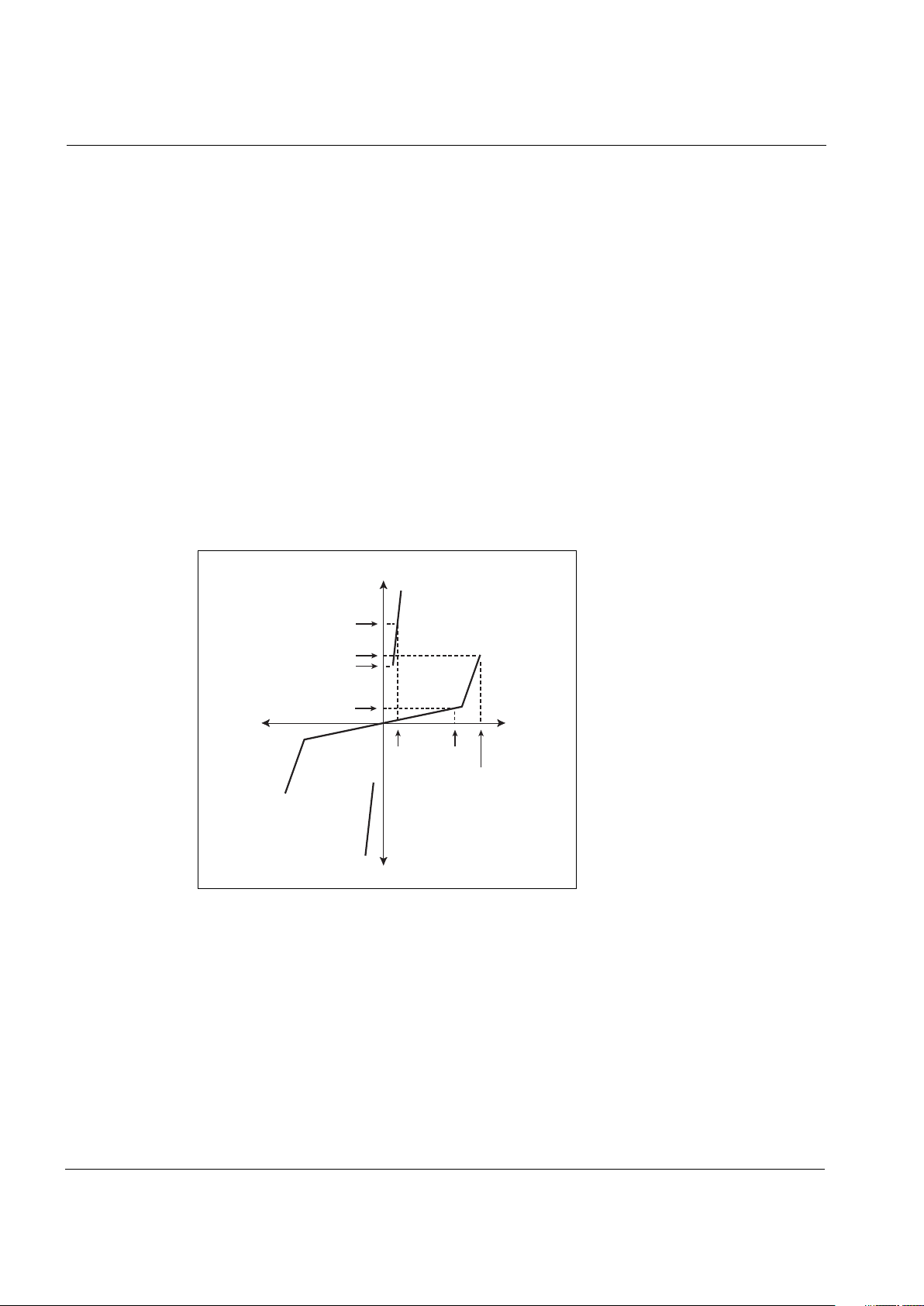
Operation
In the standby mode, SIDACtor devices exhibit a high off-state impedance, eliminating
excessive leakage currents and appearing transparent to the circuits they protect. Upon
application of a voltage exceeding the switching voltage (VS), SIDACtor devices crowbar
and simulate a short circuit condition until the current flowing through the device is either
interrupted or drops below the SIDACtor device’s holding current (I
H
). Once this occurs,
SIDACtor devices reset and return to their high off-state impedance.
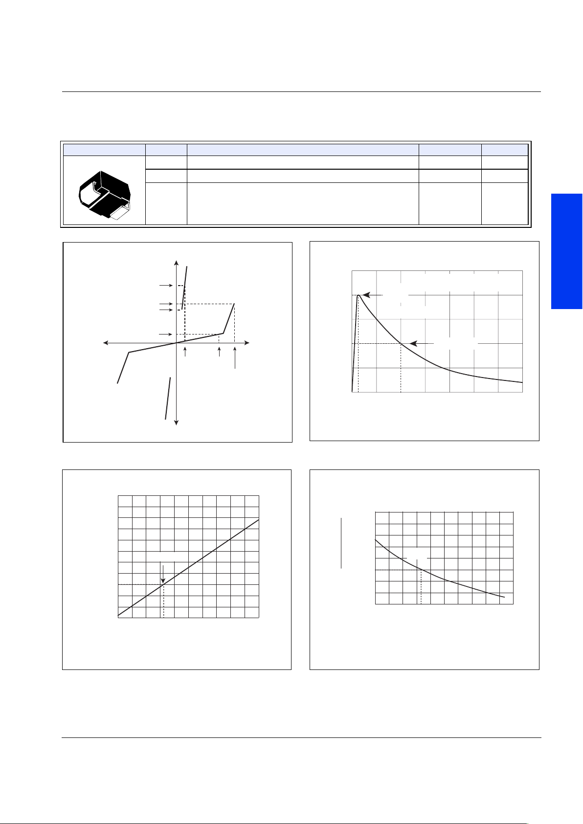
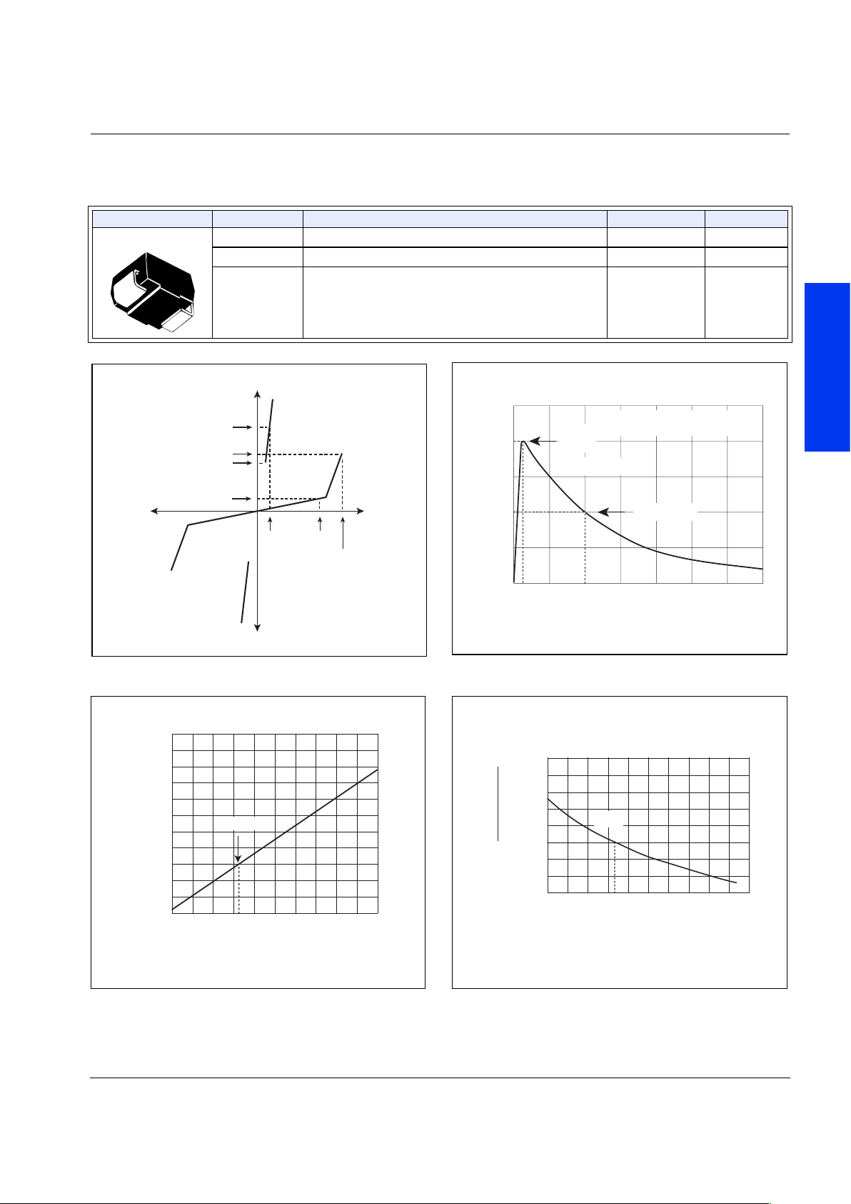
V-I Characteristics
Advantages
Compared to surge suppression using other technologies, SIDACtor devices offer absolute
surge protection regardless of the surge current available and the rate of applied voltage
(dv/dt). SIDACtor devices:
• Cannot be damaged by voltage
• Eliminate hysteresis and heat dissipation typically found with clamping devices
• Eliminate voltage overshoot caused by fast-rising transients
• Are non-degenerative
• Will not fatigue
• Have low capacitance, making them ideal for high-speed transmission equipment
I
H
I
T
I
S
I
DRM
V
DRM
V
T
+V
-V
+I
-I
V
S
Page 7

Product Description
Product Selection
Guide
© 2002 Teccor Electronics 1 - 3 http://www.teccor.com
SIDACtor
®
Data Book and Design Guide +1 972-580-7777
Applications
When protecting telecommunication circuits, SIDACtor devices are connected across Tip
and Ring for metallic protection and across Tip and Ground and Ring and Ground for
longitudinal protection. They typically are placed behind some type of current-limiting
device, such as Teccor’s F1250T Telelink slow blow fuse. Common applications include:
• Central office line cards (SLICs)
• T-1/E-1, ISDN, and xDSL transmission equipment
• Customer Premises Equipment (CPE) such as phones, modems, and caller ID adjunct
boxes
• PBXs, KSUs, and other switches
• Primary protection including main distribution frames, five-pin modules, building
entrance equipment, and station protection modules
• Data lines and security systems
• CATV line amplifiers and power inserters
• Sprinkler systems
For more information regarding specific applications, design requirements, or surge
suppression, please contact Teccor Electronics directly at +1 972-580-7777 or through our
local area representative. Access Teccor’s web site at http://www.teccor.com or
e-mail us at sidactor.techsales@teccor.com.
Page 8
Product Packages
http://www.teccor.com 1 - 4 © 2002 Teccor Electronics
+1 972-580-7777 SIDACtor
®
Data Book and Design Guide
Product Packages
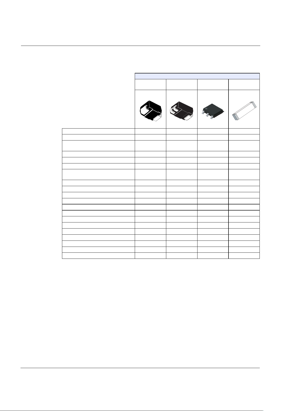
Surface Mount Packages
DO-214AA
Modified
DO-214AA
Modified
MS-013 Six-pin
Surface Mount
(Fuse)
Balanced SIDACtor Device
✓
Battrax Dual Negative SLIC Protector ✓
Battrax Dual Positive/Negative SLIC
Protector
✓
Battrax Quad Negative SLIC Protector ✓
Battrax SLIC Protector ✓✓
CATV/HFC SIDACtor Device
CATV Line Amplifiers/Power Inserters
SIDACtor Device
Fixed Voltage SLIC Protector
✓✓
Four-port Metallic Line Protector
High Surge (D-rated) SIDACtor Device ✓
LCAS Asymmetrical Device ✓✓
Longitudinal Protector ✓✓
MC Balanced SIDACtor Device ✓
MC SIDACtor Device ✓✓
Multiport Balanced SIDACtor Device ✓
Multiport Quad SLIC Protector ✓
Multiport SIDACtor Device ✓
SIDACtor Device ✓✓✓
TeleLink Fuse ✓
Twin SLIC Protector ✓
Page 9
Product Packages
Product Selection
Guide
© 2002 Teccor Electronics 1 - 5 http://www.teccor.com
SIDACtor
®
Data Book and Design Guide +1 972-580-7777
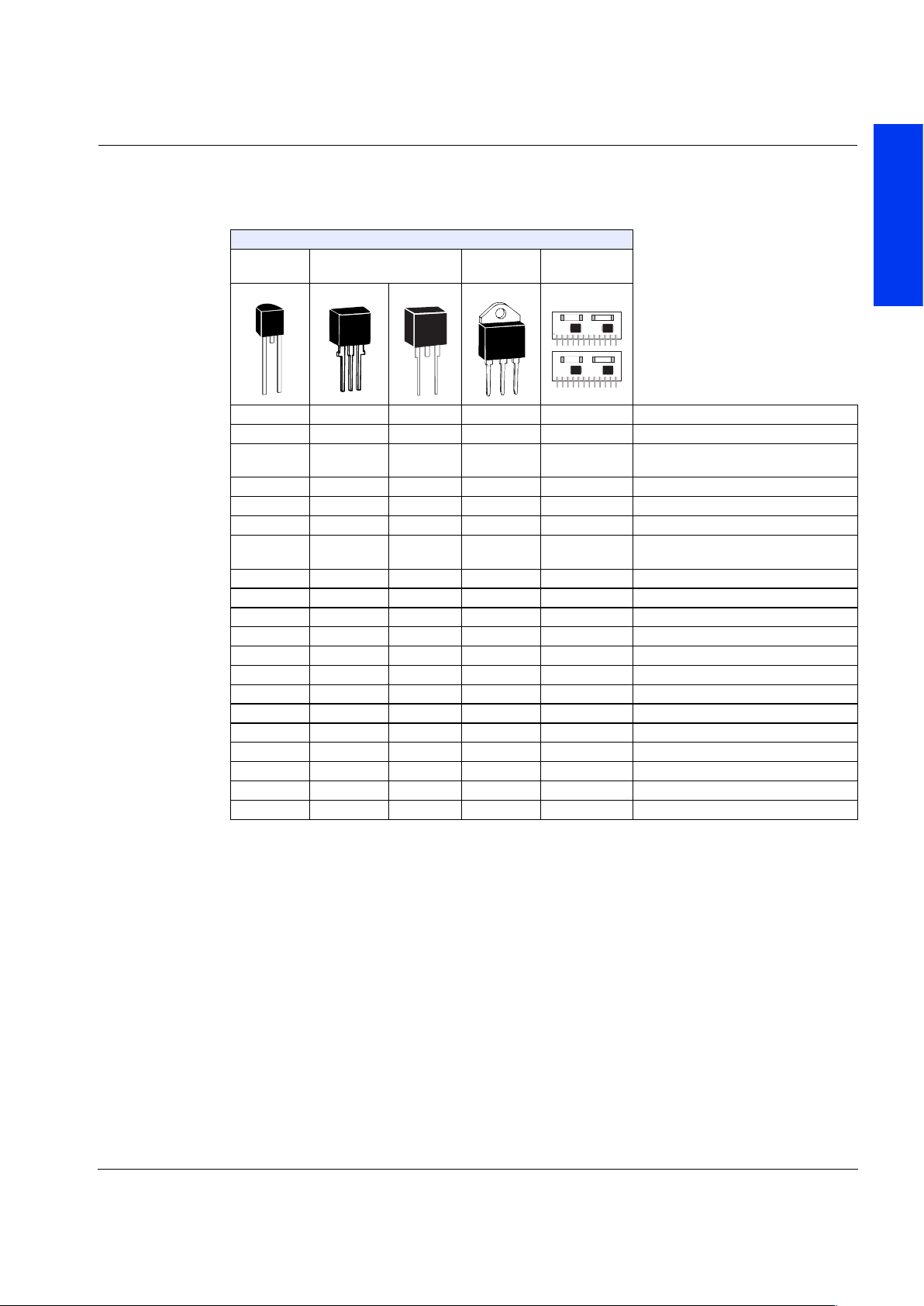
Through-hole Packages
TO-92
Modified
TO-220 TO-218 Hybrid SIP
✓✓Balanced SIDACtor Device
Battrax Dual Negative SLIC Protector
Battrax Dual Positive/Negative SLIC
Protector
Battrax Quad Negative SLIC Protector
Battrax SLIC Protector
✓✓ CATV/HFC SIDACtor Device
✓✓ CATV Line Amplifiers/Power Inserters
SIDACtor Device
✓ Fixed Voltage SLIC Protector
✓ Four-port Metallic Line Protector
✓ High Surge (D-rated) SIDACtor Device
LCAS Asymmetrical Device
✓✓Longitudinal Protector
✓✓MC Balanced SIDACtor Device
✓✓✓ ✓MC SIDACtor Device
✓ Multiport Balanced SIDACtor Device
Multiport Quad SLIC Protector
✓ Multiport SIDACtor Device
✓✓✓ ✓SIDACtor Device
✓ TeleLink Fuse
Twin SLIC Protector
Page 10

Part Number Index
http://www.teccor.com 1 - 6 © 2002 Teccor Electronics
+1 972-580-7777 SIDACtor
®
Data Book and Design Guide
Part Number Index
Note: For explanation of part numbers, see "Description of Part Number" on page 1-8.
Part Number Page
A1220U_4 2-36
A1225U_4 2-36
A2106A_ 2-32
A2106U_ 2-20
A2106U_6 2-24
A2106Z_ 2-40
A5030A_ 2-32
A5030U_ 2-20
A5030U_6 2-24
A5030Z_ 2-40
B1100C_ 2-52
B1101U_ 2-54
B1101U_4 2-58
B1160C_ 2-52
B1161U_ 2-54
B1161U_4 2-58
B1200C_ 2-52
B1201U_ 2-54
B1201U_4 2-58
B2050C_ 2-52
B3104U_ 2-56
B3164U_ 2-56
B3204U_ 2-56
F0500T 2-66
F1250T 2-66
F1251T 2-66
P0080E_ 2-16
P0080S_ 2-4
P0080SA MC 2-8
P0080SC MC 2-6
P0080SD 2-10
P0080Z_ 2-44
P0084U_ 2-22
P0300E_ 2-16
P0300S_ 2-4
P0300SA MC 2-8
P0300SC MC 2-6
P0300SD 2-10
P0300Z_ 2-44
P0304U_ 2-22
P0602A_ 2-28
P0602AC MC 2-30
P0602Z_ 2-42
P0640E_ 2-16
P0640EC MC 2-18
P0640S_ 2-4
P0640SC MC 2-6
P0640SD 2-10
P0640Z_ 2-44
P0641CA2 2-48
P0641S_ 2-46
P0641U_ 2-50
P0642S_ 2-14
P0644U_ 2-22
P0720E_ 2-16
P0720S_ 2-4
P0720SC MC 2-6
P0720SD 2-10
P0720Z_ 2-44
P0721CA2 2-48
P0721S_ 2-46
P0721U_ 2-50
P0722S_ 2-14
P0724U_ 2-22
P0900E_ 2-16
P0900S_ 2-4
P0900SC MC 2-6
P0900SD 2-10
P0900Z_ 2-44
P0901CA2 2-48
P0901S_ 2-46
P0901U_ 2-50
P0902S_ 2-14
P0904U_ 2-22
P1100E_ 2-16
P1100S_ 2-4
P1100SC MC 2-6
P1100SD 2-10
P1100Z_ 2-44
P1101CA2 2-48
Part Number Page
P1101S_ 2-46
P1101U_ 2-50
P1102S_ 2-14
P1104U_ 2-22
P1200S_ 2-38
P1300E_ 2-16
P1300S_ 2-4
P1300SC MC 2-6
P1300SD 2-10
P1300Z_ 2-44
P1304U_ 2-22
P1400AD 2-60
P1402A_ 2-28
P1402AC MC 2-30
P1402Z_ 2-42
P1500E_ 2-16
P1500EC MC 2-18
P1500S_ 2-4
P1500SC MC 2-6
P1500SD 2-10
P1500Z_ 2-44
P1504U_ 2-22
P1553A_ 2-32
P1553AC MC 2-34
P1553U_ 2-20
P1553Z_ 2-40
P1556U_ 2-24
P1602A_ 2-28
P1602AC MC 2-30
P1602Z_ 2-42
P1800AD 2-60
P1800E_ 2-16
P1800S_ 2-4
P1800SC MC 2-6
P1800SD 2-10
P1800Z_ 2-44
P1803A_ 2-32
P1803AC MC 2-34
P1803U_ 2-20
P1803Z_ 2-40
Part Number Page
Page 11

Part Number Index
© 2002 Teccor Electronics 1-7 http://www.teccor.com
SIDACtor
®
Data Book and Design Guide +1 972-580-7777
Product Selection
Guide
P1804U_ 2-22
P1806U_ 2-24
P1900ME 2-64
P2000AA61 2-26
P2000S_ 2-38
P2103A_ 2-32
P2103AC MC 2-34
P2103U_ 2-20
P2103Z_ 2-40
P2106U_ 2-24
P2200AA61 2-26
P2202A_ 2-28
P2202AC MC 2-30
P2202Z_ 2-42
P2300E_ 2-16
P2300ME 2-64
P2300S_ 2-4
P2300SC MC 2-6
P2300SD 2-10
P2300Z_ 2-44
P2304U_ 2-22
P2353A_ 2-32
P2353AC MC 2-34
P2353U_ 2-20
P2353Z_ 2-40
P2356U_ 2-24
P2400AA61 2-26
P2500AA61 2-26
P2500S_ 2-38
P2600E_ 2-16
P2600EC MC 2-18
P2600S_ 2-4
P2600SC MC 2-6
P2600SD 2-10
P2600Z_ 2-44
P2604U_ 2-22
P2702A_ 2-28
P2702AC MC 2-30
P2702Z_ 2-42
P2703A_ 2-32
Part Number Page
P2703AC MC 2-34
P2703U_ 2-20
P2703Z_ 2-40
P2706U_ 2-24
P3000AA61 2-26
P3002A_ 2-28
P3002AC MC 2-30
P3002CA 2-12
P3002S_ 2-14
P3002Z_ 2-42
P3100AD 2-62
P3100E_ 2-16
P3100EC MC 2-18
P3100S_ 2-4
P3100SC MC 2-6
P3100SD 2-10
P3104U_ 2-22
P3100Z_ 2-44
P3203A_ 2-32
P3203AC MC 2-34
P3203U_ 2-20
P3203Z_ 2-40
P3206U_ 2-24
P3300AA61 2-26
P3403A_ 2-32
P3403AC MC 2-34
P3403U_ 2-20
P3403Z_ 2-40
P3406U_ 2-24
P3500E_ 2-16
P3500S_ 2-4
P3500SC MC 2-6
P3500SD 2-10
P3500Z_ 2-44
P3504U_ 2-22
P3602A_ 2-28
P3602AC MC 2-30
P3602Z_ 2-42
P4202A_ 2-28
P4202AC MC 2-30
Part Number Page
P4202Z_ 2-42
P4802A_ 2-28
P4802AC MC 2-30
P4802Z_ 2-42
P5103A_ 2-32
P5103AC MC 2-34
P5103U_ 2-20
P5106U_ 2-24
P6002A_ 2-28
P6002AC MC 2-30
P6002AD 2-62
P6002CA 2-12
P6002Z_ 2-42
Part Number Page
Page 12
Description of Part Number
http://www.teccor.com 1 - 8 © 2002 Teccor Electronics
+1 972-580-7777 SIDACtor
®
Data Book and Design Guide
Description of Part Number
The following illustration shows a description of a sample SIDACtor device part number.
P 210 2 A A
DEVICE TYPE
P = SIDACtor
PACKAGE TYPE
A = TO–220
C = Three-leaded DO-214
E = TO–92
M = TO-218
S = DO–214
U = Six-pin SOIC
Z = SIP
LEAD FORM OPTIONS
TO-220 modified type 60, 61, or 62
For U type:
3 = 3 chips
4 = 4 chips
6 = 6 chips
61
CONSTRUCTION VARIABLE
0 = One chip
1 = Unidirectional part
2 = Two chips
3 = Three chips
I
PP
RATING
A = 50 A (10x560 µs)
B = 100 A (10x560 µs)
C = 500 A (2x10 µs)
D = 1000 A (8x20 µs)
E = 3000 A (8x20 µs)
RP
PACKING OPTIONS
RP1 = TO-92 reel pack (0.100" lead spacing)
RP2 = TO-92 reel pack (0.200" lead spacing)
AP = Ammo pack
RP = Reel pack
TP = Tube pack
MEDIAN VOLTAGE RATING
210 = 210 V
0 = One SIDACtor Chip
2 = Two Matched SIDACtor Chips
3 = Three Matched SIDACtor Chips
Patented
1
3
2
1
3
2
Page 13

Description of Part Number
Product Selection
Guide
© 2002 Teccor Electronics 1 - 9 http://www.teccor.com
SIDACtor
®
Data Book and Design Guide +1 972-580-7777
The following illustration shows a description of a sample Battrax device part number.
The following illustration shows a description of a sample asymmetrical SIDACtor device
part number.
B1 1 U A
DEVICE TYPE
B = Battrax
PACKAGE TYPE
C = Three-leaded DO-214
U = Six-pin SOIC
CONSTRUCTION VARIABLE
0 = No diode
1 = Diode
4 = Four Battrax Devives
IPP RATING
A = 50 A (10x560 µs)
B = 100 A (10x560 µs)
C = 500 A (2x10 µs)
HOLDING CURRENT
05 = 50 mA
10 = 100 mA
16 = 160 mA
20 = 200 mA
10
Battrax TYPE
1 = Negative
2 = Positive
3 = Dual
A1806 U C
DEVICE TYPE
A = Asymmetrical SIDACtor
PACKAGE TYPE
A = TO-220
M = TO-218
U = Six-pin SOIC
LEAD FORM OPTIONS
TO-220 modified type 60, 61, or 62
For U type:
3 = 3 chips
4 = 4 chips
6 = 6 chips
4
IPP RATING
A = 50 A (10x560 µs)
B = 100 A (10x560 µs)
C = 500 A (2x10 µs)
D = 1000 A (8x20 µs)
E = 3000 A (8x20 µs)
PACKING OPTIONS
AP = Ammo pack
RP = Reel pack
TP = Tube pack
MEDIAN VOLTAGE RATING
1806 = 180 V and 60 V
TP
3 = Three Matched SIDACtor chips
Patented
1
3
2
Page 14

Electrical Parameters
http://www.teccor.com 1 - 10 © 2002 Teccor Electronics
+1 972-580-7777 SIDACtor
®
Data Book and Design Guide
Electrical Parameters
Electrical parameters are based on the following definition of conditions:
• On state (also referred to as the crowbar condition) is the low impedance condition
reached during full conduction and simulates a short circuit.
• Off state (also referred to as the blocking condition) is the high impedance condition prior
to beginning conduction and simulates an open circuit.
C
O
Off-state Capacitance — typical capacitance measured in off state
di/dt Rate of Rise of Current — maximum rated value of the acceptable rate of
rise in current over time
dv/dt Rate of Rise of Voltage — rate of applied voltage over time
I
S
Switching Current — maximum current required to switch to on state
I
DRM
Leakage Current — maximum peak off-state current measured at V
DRM
I
H
Holding Current — minimum current required to maintain on state
I
PP
Peak Pulse Current — maximum rated peak impulse current
I
T
On-state Current — maximum rated continuous on-state current
I
TSM
Peak One-cycle Surge Current — maximum rated one-cycle AC current
V
S
Switching Voltage — maximum voltage prior to switching to on state
V
DRM
Peak Off-state Voltage — maximum voltage that can be applied while
maintaining off state
V
F
On-state Forward Voltage — maximum forward voltage measured at rated
on-state current
V
T
On-state Voltage — maximum voltage measured at rated on-state current
Page 15

Quality and Reliability
Product Selection
Guide
© 2002 Teccor Electronics 1 - 11 http://www.teccor.com
SIDACtor
®
Data Book and Design Guide +1 972-580-7777
Quality and Reliability
It is Teccor’s policy to ship quality products on time. We accomplish this through Total
Quality Management based on the fundamentals of customer focus, continuous
improvement, and people involvement.
In support of this commitment, Teccor applies the following principles:
• Employees shall be respected, involved, informed, and qualified for their job with
appropriate education, training, and experience.
• Customer expectations shall be met or exceeded by consistently shipping products that
meet the agreed specifications, quality levels, quantities, schedules, and test and
reliability parameters.
• Suppliers shall be selected by considering quality, service, delivery, and cost of
ownership.
• Design of products and processes will be driven by customer needs, reliability, and
manufacturability.
It is the responsibility of management to incorporate these principles into policies and
systems.
It is the responsibility of those in leadership roles to coach their staff and to reinforce these
principles.
It is the responsibility of each individual employee to follow the spirit of this statement to
ensure that we meet the primary policy — to ship quality products on time.
Page 16

Standard Terms and Conditions
© 2002 Teccor Electronics 1 - 12 http://www.teccor.com
SIDACtor
®
Data Book and Design Guide +1 972-580-7777
Standard Terms and Conditions
Supplier shall not be bound by any term proposed by Buyer in the absence of written agreement to such term signed by an
authorized officer of Supplier.
(1) PRICE:
(A) Supplier reserves the right to change product prices at any time but, whenever practicable, Supplier will give Buyer at
least thirty (30) days written notice before the effective date of any price change. Unless Supplier has specifically
agreed in writing, signed by an authorized officer of Supplier, that a quoted price shall not be subject to change for a
certain time, all products shipped on or after the effective date of a price change may be billed at the new price level.
(B) Whenever Supplier agrees to a modification of Buyer's order (which modification must be in writing and signed by an
authorized officer of Supplier), Supplier reserves the right to alter its price, whether or not such price was quoted
as “firm”.
(C) Prices do not include federal, state or local taxes, now or hereafter enacted, applicable to the goods sold. Taxes will
be added by Supplier to the sales prices whenever Supplier has legal obligation to collect them and will be paid by
Buyer as invoiced unless Buyer provides Supplier with a proper tax exemption certificate.
(2) PRODUCTION: Supplier may, at its sole discretion and at any time, withdraw any catalog item from further production without
notice or liability to Buyer.
(3) INTEREST:
(A) All late payments shall bear interest thirty (30) days after the due date stated on the invoice until paid at the lower of one
and one-half percent per month or the maximum rate permitted by law. All interest becoming due shall, if not paid when
due, be added to principal and bear interest from the due date. At Supplier's option, any payment shall be applied first
to interest and then to principal.
(B) It is the intention of the parties to comply with the laws of the jurisdiction governing any agreement between the
parties relating to interest. If any construction of the agreement between the parties indicates a different right given
to Supplier to demand or receive any sum greater than that permissible by law as interest, such as a mistake in
calculation or wording, this paragraph shall override. In any contingency which will cause the interest paid or
agreed to be paid to exceed the maximum rate permitted by law, such excess will be applied to the reduction of
any principal amount due, or if there is no principal amount due, shall be refunded.
(4) TITLE AND DELIVERY: Title to goods ordered by Buyer and risk of loss or damage in transit or thereafter shall pass to Buyer
upon Supplier's delivery of the goods at Supplier's plant or to a common carrier for shipment to Buyer.
(5) CONTINGENCIES: Supplier shall not be responsible for any failure to perform due to causes reasonably beyond its control.
These causes shall include, but not be restricted to, fire, storm, flood, earthquake, explosion, accident, acts of public enemy,
war rebellion, insurrection, sabotage, epidemic, quarantine restrictions, labor disputes, labor shortages, labor slow downs
and sit downs, transportation embargoes, failure or delays in transportation, inability to secure raw materials or machinery for
the manufacture of its devices, acts of God, acts of the Federal Government or any agency thereof, acts of any state or local
government or agency thereof, and judicial action. Similar causes shall excuse Buyer for failure to take goods ordered by
Buyer, from the time Supplier receives written notice from Buyer and for as long as the disabling cause continues, other than
for goods already in transit or specially fabricated and not readily saleable to other buyers.
Supplier assumes no responsibility for any tools, dies, and other equipment furnished Supplier by Buyer.
(6) LIMITED WARRANTY AND EXCLUSIVE REMEDY: Supplier warrants all catalog products to be free from defects in materials
and workmanship under normal and proper use and application for a period of twelve (12) months from the date code on the
product in question (or if none, from the date of delivery to Buyer.) With respect to products assembled, prepared, or manufactured to Buyer's specifications, Supplier warrants only that such products will meet Buyer's specifications upon delivery.
As the party responsible for the specifications, Buyer shall be responsible for testing and inspecting the products for adherence to specifications, and Supplier shall have no liability in the absence of such testing and inspection or if the product
passes such testing or inspection. THE ABOVE WARRANTY IS THE ONLY WARRANTY EXTENDED BY SUPPLIER, AND
IS IN LIEU OF AND EXCLUDES ALL OTHER WARRANTIES AND CONDITIONS, EXPRESSED OR IMPLIED (EXCEPT AS
PROVIDED HEREIN AS TO TITLE), ON ANY GOODS OR SERVICES SOLD OR RENDERED BY SUPPLIER, INCLUDING
ANY IMPLIED WARRANTIES OF MERCHANTABILITY AND FITNESS FOR A PARTICULAR PURPOSE. THIS WARRANTY
WILL NOT CREATE WARRANTY COVERAGE FOR ANY ITEM INTO WHICH ANY PRODUCT SOLD BY SUPPLIER MAY
HAVE BEEN INCORPORATED OR ADDED.
SUPPLIER'S ENTIRE LIABILITY AND BUYER'S EXCLUSIVE REMEDY UNDER THIS WARRANTY SHALL BE, AT
SUPPLIER'S OPTION, EITHER THE REPLACEMENT OF, REPAIR OF, OR ISSUANCE OF CREDIT TO BUYER'S
ACCOUNT WITH SUPPLIER FOR ANY PRODUCTS WHICH ARE PROPERLY RETURNED BY BUYER DURING THE
WARRANTY PERIOD. All returns must comply with the following conditions:
Page 17

Standard Terms and Conditions
Product Selection
Guide
© 2002 Teccor Electronics 1 - 13 http://www.teccor.com
SIDACtor
®
Data Book and Design Guide +1 972-580-7777
(A) Supplier is to be promptly notified in writing upon discovery of defects by Buyer.
(B) Buyer must obtain a Return Material Authorization (RMA) number from the Supplier prior to returning product.
(C) The defective product is returned to Supplier, transportation charges prepaid by Buyer.
(D) Supplier's examination of such product discloses, to its satisfaction, that such defects have not been caused by
misuse, neglect, improper installation, repair, alteration, or accident.
(E) The product is returned in the form it was delivered with any necessary disassembly carried out by Buyer at Buyer's
expense.
IN NO EVENT SHALL SUPPLIER, OR ANYONE ELSE ASSOCIATED IN THE CREATION OF ANY OF SUPPLIER'S
PRODUCTS OR SERVICES, BE LIABLE TO BUYER FOR INCIDENTAL OR CONSEQUENTIAL DAMAGES OF ANY
NATURE INCLUDING LOSS OF PROFITS, LOSS OF USE, BUSINESS INTERUPTION, AND THE LIKE. BUYER
ACKNOWLEDGES THAT THE ABOVE WARRANTIES AND LIMITATIONS THEREON ARE APPROPRIATE AND
REASONABLE IN EFFECTUATING SUPPLIER'S AND BUYER'S MUTUAL INTENTION TO CONDUCT AN EFFICIENT
TRANSACTION AT PRICES MORE ADVANTAGEOUS TO BUYER THAN WOULD BE AVAILABLE IN THE PRESENCE
OF OTHER WARRANTIES AND ASSURANCES.
(7) PATENTS: Buyer shall notify Supplier in writing of any claim that any product or any part of use thereof furnished under this
agreement constitutes an infringement of any U.S. patent, copyright, trade secret, or other proprietary rights of a third party.
Notice shall be given within a reasonable period of time which should in most cases be within ten (10) days of receipt by
Buyer of any letter, summons, or complaint pertaining to such a claim. At its option, Supplier may defend at its expense any
action brought against Buyer to the extent that it is based on such a claim. Should Supplier choose to defend any such claim,
Supplier may fully participate in the defense, settlement, or appeal of any action based on such claim.
Should any product become, or in Supplier's opinion be likely to become, the subject of an action based on any such
claim, Supplier may, at its option, as the Buyer's exclusive remedy, either procure for the Buyer the right to continue
using the product, replace the product or modify the product to make it noninfringing. IN NO EVENT SHALL SUPPLIER
BE LIABLE FOR ANY INCIDENTAL OR CONSEQUENTIAL DAMAGES BASED ON ANY CLAIM OF INFRINGEMENT.
Supplier shall have no liability for any claim based on modifications of a product made by any person or entity other than
Supplier, or based on use of a product in conjunction with any other item, unless expressly approved by Supplier.
Supplier does not warrant goods against claims of infringement which are assembled, prepared, or manufactured to
Buyer's specifications.
(8) NON-WAIVER OF DEFAULT: Each shipment made under any order shall be treated as a separate transaction, but in the
event of any default by Buyer, Supplier may decline to make further shipments without in any way affecting its rights under
such order. If, despite any default by Buyer, Supplier elects to continue to make shipments, its action shall not constitute a
waiver of that or any default by Buyer or in any way affect Supplier's legal remedies for any such default. At any time, Supplier's failure to exercise any right to remedy available to it shall not constitute a waiver of that right or remedy.
(9) TERMINATION: If the products to be furnished under this order are to be used in the performance of a Government contract
or subcontract, and the Government terminates such contract in whole or part, this order may be canceled to the extent it
was to be used in the canceled portion of said Government contract and the liability of Buyer for termination allowances shall
be determined by the then applicable regulations of the Government regarding termination of contracts. Supplier may cancel
any unfilled orders unless Buyer shall, upon written notice, immediately pay for all goods delivered or shall pay in advance
for all goods ordered but not delivered, or both, at Supplier's option.
(10) LAW: The validity, performance and construction of these terms and conditions and any sale made hereunder shall be gov-
erned by the laws of the state of Texas.
(11) ASSIGNS: This agreement shall not be assignable by either Supplier or Buyer. However, should either Supplier or Buyer be
sold or transferred in its entirety and as an ongoing business, or should Supplier or Buyer sell or transfer in its entirety and as
an ongoing concern, any division, department, or subsidiary responsible in whole or in part for the performance of this Agreement, this Agreement shall be binding upon and inure to the benefit of those successors and assigns of Supplier, Buyer, or
such division, department, or subsidiary.
(12) MODIFICATION OF STANDARD TERMS AND CONDITIONS: No attempted or suggested modification of or addition to any
of the provisions upon the face or reverse of this form, whether contained or arising in correspondence and/or documents
passing between Supplier and Buyer, in any course of dealing between Supplier or Buyer, or in any customary usage prevalent among businesses comparable to those of Supplier and/or Buyer, shall be binding upon Supplier unless made and
agreed to in writing and signed by an officer of Supplier.
(13) QUANTITIES: Any variation in quantities of electronic components, or other goods shipped over or under the quantities
ordered (not to exceed 5%) shall constitute compliance with Buyer's order and the unit price will continue to apply.
Page 18

NOTES
Page 19

© 2002 Teccor Electronics 2-1 http://www.teccor.com
SIDACtor
®
Data Book and Design Guide +1 972-580-7777
Data Sheets
2 Data Sheets
This section presents complete electrical specifications for Teccor’s SIDACtor solid state
overvoltage protection devices.
DO-214AA Package Symbolization. . . . . . . . . . . . . . . . . . . . . . . . . . . . . . . . . . . . . . . . . . . . . . . . . . . . . 2-3
DO-214AA
SIDACtor Device . . . . . . . . . . . . . . . . . . . . . . . . . . . . . . . . . . . . . . . . . . . . . . . . . . . . . . . . . . . . . . 2-4
MicroCapacitance (MC) SC SIDACtor Device . . . . . . . . . . . . . . . . . . . . . . . . . . . . . . . . . . . . . . . . 2-6
MicroCapacitance (MC) SA SIDACtor Device . . . . . . . . . . . . . . . . . . . . . . . . . . . . . . . . . . . . . . . . 2-8
High Surge Current (D-rated) SIDACtor Device. . . . . . . . . . . . . . . . . . . . . . . . . . . . . . . . . . . . . . 2-10
Compak Two-chip SIDACtor Device . . . . . . . . . . . . . . . . . . . . . . . . . . . . . . . . . . . . . . . . . . . . . . 2-12
Ethernet/10BaseT/100BaseT Protector . . . . . . . . . . . . . . . . . . . . . . . . . . . . . . . . . . . . . . . . . . . . 2-14
TO-92
SIDACtor Device . . . . . . . . . . . . . . . . . . . . . . . . . . . . . . . . . . . . . . . . . . . . . . . . . . . . . . . . . . . . . 2-16
MicroCapacitance (MC) SIDACtor Device . . . . . . . . . . . . . . . . . . . . . . . . . . . . . . . . . . . . . . . . . . 2-18
Modified MS-013 (Six-pin Surface Mount)
Balanced Three-chip SIDACtor Device . . . . . . . . . . . . . . . . . . . . . . . . . . . . . . . . . . . . . . . . . . . . 2-20
Multiport SIDACtor Device . . . . . . . . . . . . . . . . . . . . . . . . . . . . . . . . . . . . . . . . . . . . . . . . . . . . . . 2-22
Multiport Balanced SIDACtor Device . . . . . . . . . . . . . . . . . . . . . . . . . . . . . . . . . . . . . . . . . . . . . . 2-24
Modified TO-220
SIDACtor Device . . . . . . . . . . . . . . . . . . . . . . . . . . . . . . . . . . . . . . . . . . . . . . . . . . . . . . . . . . . . . 2-26
Two-chip SIDACtor Device. . . . . . . . . . . . . . . . . . . . . . . . . . . . . . . . . . . . . . . . . . . . . . . . . . . . . . 2-28
Two-chip MicroCapacitance (MC) SIDACtor Device . . . . . . . . . . . . . . . . . . . . . . . . . . . . . . . . . . 2-30
Balanced Three-chip SIDACtor Device . . . . . . . . . . . . . . . . . . . . . . . . . . . . . . . . . . . . . . . . . . . . 2-32
Balanced Three-chip MicroCapacitance (MC) SIDACtor Device . . . . . . . . . . . . . . . . . . . . . . . . . 2-34
LCAS
LCAS Asymmetrical Multiport Device . . . . . . . . . . . . . . . . . . . . . . . . . . . . . . . . . . . . . . . . . . . . . 2-36
LCAS Asymmetrical Discrete Device . . . . . . . . . . . . . . . . . . . . . . . . . . . . . . . . . . . . . . . . . . . . . . 2-38
SIP Hybrid Overvoltage and Overcurrent Protector
Four-Port Balanced Three-chip Protector . . . . . . . . . . . . . . . . . . . . . . . . . . . . . . . . . . . . . . . . . . 2-40
Four-Port Longitudinal Two-chip Protector. . . . . . . . . . . . . . . . . . . . . . . . . . . . . . . . . . . . . . . . . . 2-42
Four-Port Metallic Line Protector . . . . . . . . . . . . . . . . . . . . . . . . . . . . . . . . . . . . . . . . . . . . . . . . . 2-44
SLICs
Fixed Voltage SLIC Protector . . . . . . . . . . . . . . . . . . . . . . . . . . . . . . . . . . . . . . . . . . . . . . . . . . . . 2-46
Twin SLIC Protector . . . . . . . . . . . . . . . . . . . . . . . . . . . . . . . . . . . . . . . . . . . . . . . . . . . . . . . . . . . 2-48
Multiport SLIC Protector. . . . . . . . . . . . . . . . . . . . . . . . . . . . . . . . . . . . . . . . . . . . . . . . . . . . . . . . 2-50
Battrax
Battrax SLIC Protector . . . . . . . . . . . . . . . . . . . . . . . . . . . . . . . . . . . . . . . . . . . . . . . . . . . . . . . . . 2-52
Battrax Dual Negative SLIC Protector . . . . . . . . . . . . . . . . . . . . . . . . . . . . . . . . . . . . . . . . . . . . . 2-54
Battrax Dual Positive/Negative SLIC Protector . . . . . . . . . . . . . . . . . . . . . . . . . . . . . . . . . . . . . . 2-56
Battrax Quad Negative SLIC Protector . . . . . . . . . . . . . . . . . . . . . . . . . . . . . . . . . . . . . . . . . . . . 2-58
CATVs
CATV and HFC SIDACtor Device . . . . . . . . . . . . . . . . . . . . . . . . . . . . . . . . . . . . . . . . . . . . . . . . 2-60
High Surge Current SIDACtor Device . . . . . . . . . . . . . . . . . . . . . . . . . . . . . . . . . . . . . . . . . . . . . 2-62
CATV Line Amplifiers/Power Inserters SIDACtor Device . . . . . . . . . . . . . . . . . . . . . . . . . . . . . . . 2-64
TeleLink Fuse . . . . . . . . . . . . . . . . . . . . . . . . . . . . . . . . . . . . . . . . . . . . . . . . . . . . . . . . . . . . . . . . . . . . 2-66
Acronyms: CATV Community Antenna TV
HFC Hybrid Fiber Coax
LCAS Line Circuit Access Switch
SIP Single In-line Package
SLIC Subscriber Line Interface Circuit
Page 20

Page 21

DO-214AA Package Symbolization
© 2002 Teccor Electronics 2 - 3 http://www.teccor.com
SIDACtor
®
Data Book and Design Guide +1 972-580-7777
Data Sheets
DO-214AA Package Symbolization
Note: Date code is located below the symbolized part number.
Part Number Part Number Part Number
Catalog Symbolized Catalog Symbolized Catalog Symbolized
P0080SA P-8A P0901SC P91C P2300SB P23B
P0080SA MC P-8AM P1100SA P11A P2300SC P23C
P0080SB P-8B P1100SB P11B P2300SD P23D
P0080SC P-8C P1100SC P11C P2300SC MC P23CM
P0080SD P-8D P1100SD P11D P2500SA P25A
P0080SC MC P-8CM P1100SC MC P11CM P2500SB P25B
P0300SA P03A P1101CA2 P02A P2500SC P25C
P0300SA MC P03AM P1101SA P01A P2500SD P25D
P0300SB P03B P1101SC P01C P2500SC MC P25CM
P0300SC P03C P1200SA P12A P2600SA P26A
P0300SD P03D P1200SB P12B P2600SB P26B
P0300SC MC P03CM P1200SC P12C P2600SC P26C
P0640SA P06A P1200SD P12D P2600SD P26D
P0640SB P06B P1200SC MC P12CM P2600SC MC P26CM
P0640SC P06C P1300SA P13A P3002CB P30B
P0640SD P06D P1300SB P13B P3002SB P30B
P0640SC MC P06CM P1300SC P13C P3100SA P31A
P0641CA2 P62A P1300SD P13D P3100SB P31B
P0641SA P61A P1300SC MC P13CM P3100SC P31C
P0641SC P61C P1500SA P15A P3100SD P31D
P0720SA P07A P1500SB P15B P3100SC MC P31CM
P0720SB P07B P1500SC P15C P3500SA P35A
P0720SC P07C P1500SD P15D P3500SB P35B
P0720SD P07D P1500SC MC P15CM P3500SC P35C
P0720SC MC P07CM P1800SA P18A P3500SD P35D
P0721CA2 P72A P1800SB P18B P3500SC MC P35CM
P0721SA P71A P1800SC P18C P6002CB P60B
P0721SC P71C P1800SD P18D B1100CA B10A
P0900SA P09A P1800SC MC P18CM B1100CC B10C
P0900SB P09B P2000SA P20A B1160CA B16A
P0900SC P09C P2000SB P20B B1160CC B16C
P0900SD P09D P2000SC P20C B1200CA B12A
P0900SC MC P09CM P2000SD P20D B1200CC B12C
P0901CA2 P92A P2000SC MC P20CM B2050CA B25A
P0901SA P91A P2300SA P23A B2050CC B25C
Page 22
SIDACtor Device
http://www.teccor.com 2 - 4 © 2002 Teccor Electronics
+1 972-580-7777 SIDACtor
®
Data Book and Design Guide
SIDACtor Device
DO-214AA SIDACtor solid state protection devices protect telecommunications equipment
such as modems, line cards, fax machines, and other CPE.
SIDACtor devices are used to enable equipment to meet various regulatory requirements
including GR 1089, ITU K.20, K.21 and K.45, IEC 60950, UL 60950, and TIA-968 (formerly
known as FCC Part 68).
* For individual “SA”, “SB”, and “SC” surge ratings, see table below.
General Notes:
• All measurements are made at an ambient temperature of 25 °C. I
PP
applies to -40 °C through +85 °C temperature range.
• I
PP
is a repetitive surge rating and is guaranteed for the life of the product.
• Listed SIDACtor devices are bi-directional. All electrical parameters and surge ratings apply to forward and reverse polarities.
• V
DRM
is measured at I
DRM.
• VS is measured at 100 V/µs.
• Special voltage (V
S
and V
DRM
) and holding current (IH) requirements are available upon request.
• Off-state capacitance is measured at 1 MHz with a 2 V bias and is a typical value for “SA” and “SB” product. “SC” capacitance is
approximately 2x the listed value. The off-state capacitance of the P0080SB is equal to the “SC” device.
Electrical Parameters
Part
Number *
V
DRM
Volts
V
S
Vol ts
V
T
Volts
I
DRM
µAmps
I
S
mAmps
I
T
Amps
I
H
mAmps
C
O
pF
P0080S_ 6 25 4 5 800 2.2 50 100
P0300S_ 25 40 4 5 800 2.2 50 110
P0640S_ 58 77 4 5 800 2.2 150 50
P0720S_ 65 88 4 5 800 2.2 150 50
P0900S_ 75 98 4 5 800 2.2 150 50
P1100S_ 90 130 4 5 800 2.2 150 40
P1300S_ 120 160 4 5 800 2.2 150 40
P1500S_ 140 180 4 5 800 2.2 150 40
P1800S_ 170 220 4 5 800 2.2 150 30
P2300S_ 190 260 4 5 800 2.2 150 30
P2600S_ 220 300 4 5 800 2.2 150 30
P3100S_ 275 350 4 5 800 2.2 150 30
P3500S_ 320 400 4 5 800 2.2 150 30
Surge Ratings
Series
I
PP
2x10 µs
Amps
I
PP
8x20 µs
Amps
I
PP
10x160 µs
Amps
I
PP
10x560 µs
Amps
I
PP
10x1000 µs
Amps
I
TSM
60 Hz
Amps
di/dt
Amps/µs
A 150 150 90 50 45 20 500
B 250 250 150 100 80 30 500
C 500 400 200 150 100 30 500
Page 23

SIDACtor Device
© 2002 Teccor Electronics 2 - 5 http://www.teccor.com
SIDACtor
®
Data Book and Design Guide +1 972-580-7777
Data Sheets
Thermal Considerations
Package Symbol Parameter Val ue Unit
DO-214AA T
J
Operating Junction Temperature Range -40 to +150 °C
T
S
Storage Temperature Range -65 to +150 °C
R
qJA
Thermal Resistance: Junction to Ambient 90 °C/W
I
H
I
T
I
S
I
DRM
V
DRM
V
T
+V
-V
+I
-I
V
S
I
H
I
T
I
S
I
DRM
V
DRM
V
T
+V
-V
+I
-I
V
S
V-I Characteristics
50
100
0
t
r
t
d
0
Peak
Val u e
Half Value
t – Time (µs)
I
PP
– Peak Pulse Current – %I
PP
tr = rise time to peak value
t
d
= decay time to half value
Waveform = t
r
x t
d
tr x td Pulse Wave-form
-8
-40 -20 0 20 40 60 80 100 120 140 160
-6
-4
0
2
4
6
8
10
12
14
Junction Temperature (TJ) – ˚C
Percent of V
S
Change – %
25 ˚C
Normalized VS Change versus Junction Temperature
0.4
-40 -20 0 20 40 60 80 100 120 140 160
0.6
0.8
1.0
1.2
1.4
1.6
1.8
2.0
Case Temperature (TC) – ˚C
Ratio of
I
H
I
H
(T
C
= 25 ˚C)
25 ˚C
Normalized DC Holding Current versus Case Temperature
Page 24

MicroCapacitance (MC) SC SIDACtor Device
http://www.teccor.com 2 - 6 © 2002 Teccor Electronics
+1 972-580-7777 SIDACtor
®
Data Book and Design Guide
MicroCapacitance (MC) SC SIDACtor Device
The DO-214AA SC MC SIDACtor series is intended for applications sensitive to load
values. Typically, high speed connections require a lower capacitance. C
O
values for the
MicroCapacitance device are 40% lower than a standard SC part.
This MC SIDACtor series is used to enable equipment to meet various regulatory
requirements including GR 1089, IEC 60950, UL 60950, and TIA-968 (formerly known as
FCC Part 68). Contact factory regarding ITU K.20, K.21, and K.45.
* For surge ratings, see table below.
** Contact factory for release date.
General Notes:
• All measurements are made at an ambient temperature of 25 °C. I
PP
applies to -40 °C through +85 °C temperature range.
• I
PP
is a repetitive surge rating and is guaranteed for the life of the product.
• Listed SIDACtor devices are bi-directional. All electrical parameters and surge ratings apply to forward and reverse polarities.
• V
DRM
is measured at I
DRM.
• VS is measured at 100 V/µs.
• Special voltage (V
S
and V
DRM
) and holding current (IH) requirements are available upon request.
• Off-state capacitance is measured at 1 MHz with a 2 V bias.
Electrical Parameters
Part
Number *
V
DRM
Volts
V
S
Volts
V
T
Vol ts
I
DRM
µAmps
I
S
mAmps
I
T
Amps
I
H
mAmps
C
O
pF
P0080SC MC ** 6 25 4 5 800 2.2 50 55
P0300SC MC ** 25 40 4 5 800 2.2 50 35
P0640SC MC 58 77 4 5 800 2.2 150 60
P0720SC MC 65 88 4 5 800 2.2 150 60
P0900SC MC 75 98 4 5 800 2.2 150 60
P1100SC MC 90 130 4 5 800 2.2 150 50
P1300SC MC 120 160 4 5 800 2.2 150 50
P1500SC MC 140 180 4 5 800 2.2 150 50
P1800SC MC 170 220 4 5 800 2.2 150 40
P2300SC MC 190 260 4 5 800 2.2 150 40
P2600SC MC 220 300 4 5 800 2.2 150 40
P3100SC MC 275 350 4 5 800 2.2 150 40
P3500SC MC 320 400 4 5 800 2.2 150 40
Surge Ratings
Series
I
PP
2x10 µs
Amps
I
PP
8x20 µs
Amps
I
PP
10x160 µs
Amps
I
PP
10x560 µs
Amps
I
PP
10x1000 µs
Amps
I
TSM
60 Hz
Amps
di/dt
Amps/µs
C 500 400 200 150 100 30 500
Page 25

MicroCapacitance (MC) SC SIDACtor Device
© 2002 Teccor Electronics 2 - 7 http://www.teccor.com
SIDACtor
®
Data Book and Design Guide +1 972-580-7777
Data Sheets
Thermal Considerations
Package Symbol Parameter Value Unit
DO-214AA T
J
Operating Junction Temperature Range -40 to +150 °C
T
S
Storage Temperature Range -65 to +150 °C
R
qJA
Thermal Resistance: Junction to Ambient 90 °C/W
I
H
I
T
I
S
I
DRM
V
DRM
V
T
+V
-V
+I
-I
V
S
I
H
I
T
I
S
I
DRM
V
DRM
V
T
+V
-V
+I
-I
V
S
V-I Characteristics
50
100
0
t
r
t
d
0
Peak
Val u e
Half Value
t – Time (µs)
I
PP
– Peak Pulse Current – %I
PP
tr = rise time to peak value
t
d
= decay time to half value
Waveform = t
r
x t
d
tr x td Pulse Wave-form
-8
-40 -20 0 20 40 60 80 100 120 140 160
-6
-4
0
2
4
6
8
10
12
14
Junction Temperature (TJ) – ˚C
Percent of V
S
Change – %
25 ˚C
Normalized VS Change versus Junction Temperature
0.4
-40 -20 0 20 40 60 80 100 120 140 160
0.6
0.8
1.0
1.2
1.4
1.6
1.8
2.0
Case Temperature (TC) – ˚C
Ratio of
I
H
I
H
(T
C
= 25 ˚C)
25 ˚C
Normalized DC Holding Current versus Case Temperature
Page 26

MicroCapacitance (MC) SA SIDACtor Device
http://www.teccor.com 2 - 8 © 2002 Teccor Electronics
+1 972-580-7777 SIDACtor
®
Data Book and Design Guide
MicroCapacitance (MC) SA SIDACtor Device
The DO-214AA SA MC SIDACtor series is intended for applications sensitive to load
values. Typically, high speed connections require a lower capacitance. C
O
values for the
MicroCapacitance device are 40% lower than a standard SA part.
This MC SIDACtor series is used to enable equipment to meet various regulatory
requirements including GR 1089, ITU K.20, K.21, and K.45, IEC 60950, UL 60950, and TIA968 (formerly known as FCC Part 68).
* For surge ratings, see table below.
General Notes:
• All measurements are made at an ambient temperature of 25 °C. I
PP
applies to -40 °C through +85 °C temperature range.
• I
PP
is a repetitive surge rating and is guaranteed for the life of the product.
• Listed SIDACtor devices are bi-directional. All electrical parameters and surge ratings apply to forward and reverse polarities.
• V
DRM
is measured at I
DRM.
• VS is measured at 100 V/µs.
• Special voltage (V
S
and V
DRM
) and holding current (IH) requirements are available upon request.
• Off-state capacitance is measured at 1 MHz with a 2 V bias.
Electrical Parameters
Part
Number *
V
DRM
Volts
V
S
Volts
V
T
Vol ts
I
DRM
µAmps
I
S
mAmps
I
T
Amps
I
H
mAmps
C
O
pF
P0080SA MC 6 25 4 5 800 2.2 50 45
P0300SA MC 25 40 4 5 800 2.2 50 25
Surge Ratings
Series
I
PP
2x10 µs
Amps
I
PP
8x20 µs
Amps
I
PP
10x160 µs
Amps
I
PP
10x560 µs
Amps
I
PP
10x1000 µs
Amps
I
TSM
60 Hz
Amps
di/dt
Amps/µs
A 150 150 90 50 45 20 500
Page 27
MicroCapacitance (MC) SA SIDACtor Device
© 2002 Teccor Electronics 2 - 9 http://www.teccor.com
SIDACtor
®
Data Book and Design Guide +1 972-580-7777
Data Sheets
Thermal Considerations
Package Symbol Parameter Value Unit
DO-214AA T
J
Operating Junction Temperature Range -40 to +150 °C
T
S
Storage Temperature Range -65 to +150 °C
R
qJA
Thermal Resistance: Junction to Ambient 90 °C/W
I
H
I
T
I
S
I
DRM
V
DRM
V
T
+V
-V
+I
-I
V
S
I
H
I
T
I
S
I
DRM
V
DRM
V
T
+V
-V
+I
-I
V
S
V-I Characteristics
50
100
0
t
r
t
d
0
Peak
Val u e
Half Value
t – Time (µs)
I
PP
– Peak Pulse Current – %I
PP
tr = rise time to peak value
t
d
= decay time to half value
Waveform = t
r
x t
d
tr x td Pulse Wave-form
-8
-40 -20 0 20 40 60 80 100 120 140 160
-6
-4
0
2
4
6
8
10
12
14
Junction Temperature (TJ) – ˚C
Percent of V
S
Change – %
25 ˚C
Normalized VS Change versus Junction Temperature
0.4
-40 -20 0 20 40 60 80 100 120 140 160
0.6
0.8
1.0
1.2
1.4
1.6
1.8
2.0
Case Temperature (TC) – ˚C
Ratio of
I
H
I
H
(T
C
= 25 ˚C)
25 ˚C
Normalized DC Holding Current versus Case Temperature
Page 28

High Surge Current (D-rated) SIDACtor Device
http://www.teccor.com 2 - 10 © 2002 Teccor Electronics
+1 972-580-7777 SIDACtor
®
Data Book and Design Guide
High Surge Current (D-rated) SIDACtor Device
DO-214AA SIDACtor solid state protection devices with a D surge rating protect
telecommunications equipment such as modems, line cards, fax machines, and other CPE.
These SIDACtor devices withstand simultaneous surges incurred in GR 1089 lightning
tests. (See "First Level Lightning Surge Test" on page 4-5.) Surge ratings are twice that of a
device with a C surge rating. This allows a discrete surface mount version of Teccor’s
patented “Y” configuration. (US Patent 4,905,119)
SIDACtor devices are used to enable equipment to meet various regulatory requirements
including GR 1089, ITU K.20, K.21 and K.45, IEC 60950, UL 60950, and TIA-968 (formerly
known as FCC Part 68).
* For surge ratings, see table below.
** Contact factory for release date.
General Notes:
• All measurements are made at an ambient temperature of 25 °C. I
PP
applies to -40 °C through +85 °C temperature range.
• I
PP
is a repetitive surge rating and is guaranteed for the life of the product.
• Listed SIDACtor devices are bi-directional. All electrical parameters and surge ratings apply to forward and reverse polarities.
• V
DRM
is measured at I
DRM.
• VS is measured at 100 V/µs.
• Special voltage (V
S
and V
DRM
) and holding current (IH) requirements are available upon request.
• Off-state capacitance is measured at 1 MHz with a 2 V bias and is a typical value.
Electrical Parameters
Part
Number *
V
DRM
Volts
V
S
Vol ts
V
T
Volts
I
DRM
µAmps
I
S
mAmps
I
T
Amps
I
H
mAmps
C
O
pF
P0080SD ** 6 25 4 5 800 2.2 50 200
P0300SD ** 25 40 4 5 800 2.2 50 220
P0640SD ** 58 77 4 5 800 2.2 50 100
P0720SD ** 65 88 4 5 800 2.2 50 100
P0900SD ** 75 98 4 5 800 2.2 50 100
P1100SD 90 130 4 5 800 2.2 50 80
P1300SD 120 160 4 5 800 2.2 50 80
P1500SD 140 180 4 5 800 2.2 50 80
P1800SD 170 220 4 5 800 2.2 50 60
P2300SD 190 260 4 5 800 2.2 50 60
P2600SD 220 300 4 5 800 2.2 50 60
P3100SD 275 350 4 5 800 2.2 50 60
P3500SD 320 400 4 5 800 2.2 50 60
Surge Ratings
Series
I
PP
2x10 µs
Amps
I
PP
8x20 µs
Amps
I
PP
10x160 µs
Amps
I
PP
10x560 µs
Amps
I
PP
10x1000 µs
Amps
I
TSM
60 Hz
Amps
di/dt
Amps/µs
D 1000 800 400 300 200 50 1000
Page 29
High Surge Current (D-rated) SIDACtor Device
© 2002 Teccor Electronics 2 - 11 http://www.teccor.com
SIDACtor
®
Data Book and Design Guide +1 972-580-7777
Data Sheets
Thermal Considerations
Package Symbol Parameter Val ue Unit
DO-214AA T
J
Operating Junction Temperature Range -40 to +150 °C
T
S
Storage Temperature Range -65 to +150 °C
R
qJA
Thermal Resistance: Junction to Ambient 90 °C/W
I
H
I
T
I
S
I
DRM
V
DRM
V
T
+V
-V
+I
-I
V
S
I
H
I
T
I
S
I
DRM
V
DRM
V
T
+V
-V
+I
-I
V
S
V-I Characteristics
50
100
0
t
r
t
d
0
Peak
Val u e
Half Value
t – Time (µs)
I
PP
– Peak Pulse Current – %I
PP
tr = rise time to peak value
t
d
= decay time to half value
Waveform = t
r
x t
d
tr x td Pulse Wave-form
-8
-40 -20 0 20 40 60 80 100 120 140 160
-6
-4
0
2
4
6
8
10
12
14
Junction Temperature (TJ) – ˚C
Percent of V
S
Change – %
25 ˚C
Normalized VS Change versus Junction Temperature
0.4
-40 -20 0 20 40 60 80 100 120 140 160
0.6
0.8
1.0
1.2
1.4
1.6
1.8
2.0
Case Temperature (TC) – ˚C
Ratio of
I
H
I
H
(T
C
= 25 ˚C)
25 ˚C
Normalized DC Holding Current versus Case Temperature
Page 30

Compak Two-chip SIDACtor Device
http://www.teccor.com 2 - 12 © 2002 Teccor Electronics
+1 972-580-7777 SIDACtor
®
Data Book and Design Guide
Compak Two-chip SIDACtor Device
The modified DO-214AA SIDACtor device provides low-cost, longitudinal protection.
SIDACtor devices are used to enable equipment to meet various regulatory requirements
including GR 1089, ITU K.20, K.21, and K.45, IEC 60950, UL 60950, and TIA-968 (formerly
known as FCC Part 68).
* For surge ratings, see table below.
General Notes:
• All measurements are made at an ambient temperature of 25 °C. I
PP
applies to -40 °C through +85 °C temperature range.
• I
PP
is a repetitive surge rating and is guaranteed for the life of the product.
• Listed SIDACtor devices are bi-directional. All electrical parameters and surge ratings apply to forward and reverse polarities.
• V
DRM
is measured at I
DRM.
• VS is measured at 100 V/µs.
• Special voltage (V
S
and V
DRM
) and holding current (IH) requirements are available upon request.
• Off-state capacitance is measured between Pins 1-3 at 1 MHz with a 2 V bias.
• UL 60950 creepage requirements must be considered.
Electrical Parameters
Part
Number
V
DRM
Vol ts
V
S
Vol ts
V
DRM
Vol ts
V
S
Vol ts
V
T
Vol ts
I
DRM
µAmps
I
S
mAmps
I
T
Amps
I
H
mAmps
C
O
pF
Pins1-2, 2-3 Pins 1-3 Pins 1-3
P3002CA 140 180 280 360 4 5 800 1 120 15
P6002CA 275 350 550 700 4 5 800 1 120 15
Surge Ratings
Series
I
PP
2x10 µs
Amps
I
PP
8x20 µs
Amps
I
PP
10x160 µs
Amps
I
PP
10x560 µs
Amps
I
PP
10x1000 µs
Amps
I
TSM
60 Hz
Amps
di/dt
Amps/µs
A 150 150 90 50 45 20 500
1
2
3
(T)
(R)
(G)
Page 31

Compak Two-chip SIDACtor Device
© 2002 Teccor Electronics 2 - 13 http://www.teccor.com
SIDACtor
®
Data Book and Design Guide +1 972-580-7777
Data Sheets
Thermal Considerations
Package Symbol Parameter Valu e Unit
Modified DO-214AA T
J
Operating Junction Temperature Range -40 to +150 °C
T
S
Storage Temperature Range -65 to +150 °C
R
qJA
Thermal Resistance: Junction to Ambient 85 °C/W
Pin 3
Pin 1
Pin 2
I
H
I
T
I
S
I
DRM
V
DRM
V
T
+V
-V
+I
-I
V
S
I
H
I
T
I
S
I
DRM
V
DRM
V
T
+V
-V
+I
-I
V
S
V-I Characteristics
50
100
0
t
r
t
d
0
Peak
Val u e
Half Value
t – Time (µs)
I
PP
– Peak Pulse Current – %I
PP
tr = rise time to peak value
t
d
= decay time to half value
Waveform = t
r
x t
d
tr x td Pulse Wave-form
-8
-40 -20 0 20 40 60 80 100 120 140 160
-6
-4
0
2
4
6
8
10
12
14
Junction Temperature (TJ) – ˚C
Percent of V
S
Change – %
25 ˚C
Normalized VS Change versus Junction Temperature
0.4
-40 -20 0 20 40 60 80 100 120 140 160
0.6
0.8
1.0
1.2
1.4
1.6
1.8
2.0
Case Temperature (TC) – ˚C
Ratio of
I
H
I
H
(T
C
= 25 ˚C)
25 ˚C
Normalized DC Holding Current versus Case Temperature
Page 32

Ethernet/10BaseT/100BaseT Protector
http://www.teccor.com 2 - 14 © 2002 Teccor Electronics
+1 972-580-7777 SIDACtor
®
Data Book and Design Guide
Ethernet/10BaseT/100BaseT Protector
The DO-214AA SIDACtor Ethernet protection series is intended for applications sensitive to
load values. Typically, high speed connections require a lower capacitance. C
O
values are
40% lower than standard devices.
SIDACtor devices are used to enable equipment to meet various regulatory requirements
including GR 1089, ITU K.20, K.21 and K.45, IEC 60950, UL 60950, and TIA-968 (formerly
known as FCC Part 68).
* For surge ratings, see table below.
General Notes:
• All measurements are made at an ambient temperature of 25 °C. I
PP
applies to -40 °C through +85 °C temperature range.
• I
PP
is a repetitive surge rating and is guaranteed for the life of the product.
• Listed SIDACtor devices are bi-directional. All electrical parameters and surge ratings apply to forward and reverse polarities.
• V
DRM
is measured at I
DRM.
• VS is measured at 100 V/µs.
• Special voltage (V
S
and V
DRM
) and holding current (IH) requirements are available upon request.
• Off-state capacitance is measured at 1 MHz with a 2 V bias.
** Contact factory for release date of B-rated devices.
Electrical Parameters
Part
Number *
V
DRM
Volts
V
S
Vol ts
V
T
Volts
I
DRM
µAmps
I
S
mAmps
I
T
Amps
I
H
mAmps
C
O
pF
P0642S_ 58 77 4 5 800 2.2 120 25
P0722S_ 65 88 4 5 800 2.2 120 25
P0902S_ 75 98 4 5 800 2.2 120 25
P1102S_ 90 130 4 5 800 2.2 120 20
P3002S_ 280 360 4 5 800 2.2 120 15
Surge Ratings
Series
I
PP
2x10 µs
Amps
I
PP
8x20 µs
Amps
I
PP
10x160 µs
Amps
I
PP
10x560 µs
Amps
I
PP
10x1000 µs
Amps
I
TSM
60 Hz
Amps
di/dt
Amps/µs
A 150 150 90 50 45 20 500
B** 250 250 150 100 80 30 500
Page 33

Ethernet/10BaseT/100BaseT Protector
© 2002 Teccor Electronics 2 - 15 http://www.teccor.com
SIDACtor
®
Data Book and Design Guide +1 972-580-7777
Data Sheets
Thermal Considerations
Package Symbol Parameter Val ue Unit
DO-214AA T
J
Operating Junction Temperature Range -40 to +150 °C
T
S
Storage Temperature Range -65 to +150 °C
R
qJA
Thermal Resistance: Junction to Ambient 90 °C/W
I
H
I
T
I
S
I
DRM
V
DRM
V
T
+V
-V
+I
-I
V
S
I
H
I
T
I
S
I
DRM
V
DRM
V
T
+V
-V
+I
-I
V
S
V-I Characteristics
50
100
0
t
r
t
d
0
Peak
Val u e
Half Value
t – Time (µs)
I
PP
– Peak Pulse Current – %I
PP
tr = rise time to peak value
t
d
= decay time to half value
Waveform = t
r
x t
d
tr x td Pulse Wave-form
-8
-40 -20 0 20 40 60 80 100 120 140 160
-6
-4
0
2
4
6
8
10
12
14
Junction Temperature (TJ) – ˚C
Percent of V
S
Change – %
25 ˚C
Normalized VS Change versus Junction Temperature
0.4
-40 -20 0 20 40 60 80 100 120 140 160
0.6
0.8
1.0
1.2
1.4
1.6
1.8
2.0
Case Temperature (TC) – ˚C
Ratio of
I
H
I
H
(T
C
= 25 ˚C)
25 ˚C
Normalized DC Holding Current versus Case Temperature
Page 34

SIDACtor Device
http://www.teccor.com 2 - 16 © 2002 Teccor Electronics
+1 972-580-7777 SIDACtor
®
Data Book and Design Guide
SIDACtor Device
TO-92 SIDACtor solid state protection devices protect telecommunications equipment such
as modems, line cards, fax machines, and other CPE.
SIDACtor devices are used to enable equipment to meet various regulatory requirements
including GR 1089, ITU K.20, K.21, and K.45, IEC 60950, UL 60950, and TIA-968 (formerly
known as FCC Part 68)
.
* For individual “EA”, “EB”, and “EC” surge ratings, see table below.
General Notes:
• All measurements are made at an ambient temperature of 25 °C. I
PP
applies to -40 °C through +85 °C temperature range.
• I
PP
is a repetitive surge rating and is guaranteed for the life of the product.
• Listed SIDACtor devices are bi-directional. All electrical parameters and surge ratings apply to forward and reverse polarities.
• V
DRM
is measured at I
DRM.
• VS is measured at 100 V/µs.
• Special voltage (V
S
and V
DRM
) and holding current (IH) requirements are available upon request.
• Off-state capacitance is measured at 1 MHz with a 2 V bias and is a typical value for “EA” and “EB” product. “EC” capacitance is
approximately 2x the listed value. The off-state capacitance of the P0080EB is equal to the “EC” device.
Electrical Parameters
Part
Number *
V
DRM
Volts
V
S
Volts
V
T
Volts
I
DRM
µAmps
I
S
mAmps
I
T
Amps
I
H
mAmps
C
O
pF
P0080E_ 6 25 4 5 800 2.2 50 100
P0300E_ 25 40 4 5 800 2.2 50 110
P0640E_ 58 77 4 5 800 2.2 150 50
P0720E_ 65 88 4 5 800 2.2 150 50
P0900E_ 75 98 4 5 800 2.2 150 50
P1100E_ 90 130 4 5 800 2.2 150 40
P1300E_ 120 160 4 5 800 2.2 150 40
P1500E_ 140 180 4 5 800 2.2 150 40
P1800E_ 170 220 4 5 800 2.2 150 30
P2300E_ 190 260 4 5 800 2.2 150 30
P2600E_ 220 300 4 5 800 2.2 150 30
P3100E_ 275 350 4 5 800 2.2 150 30
P3500E_ 320 400 4 5 800 2.2 150 30
Surge Ratings
Series
I
PP
2x10 µs
Amps
I
PP
8x20 µs
Amps
I
PP
10x160 µs
Amps
I
PP
10x560 µs
Amps
I
PP
10x1000 µs
Amps
I
TSM
60 Hz
Amps
di/dt
Amps/µs
A 150 150 90 50 45 20 500
B 250 250 150 100 80 30 500
C 500 400 200 150 100 50 500
Page 35

SIDACtor Device
© 2002 Teccor Electronics 2 - 17 http://www.teccor.com
SIDACtor
®
Data Book and Design Guide +1 972-580-7777
Data Sheets
Thermal Considerations
Package Symbol Parameter Val ue Unit
TO-92
T
J
Operating Junction Temperature Range -40 to +150 °C
T
S
Storage Temperature Range -65 to +150 °C
R
qJA
Thermal Resistance: Junction to Ambient 90 °C/W
I
H
I
T
I
S
I
DRM
V
DRM
V
T
+V
-V
+I
-I
V
S
I
H
I
T
I
S
I
DRM
V
DRM
V
T
+V
-V
+I
-I
V
S
V-I Characteristics
50
100
0
t
r
t
d
0
Peak
Val u e
Half Value
t – Time (µs)
I
PP
– Peak Pulse Current – %I
PP
tr = rise time to peak value
t
d
= decay time to half value
Waveform = t
r
x t
d
tr x td Pulse Wave-form
-8
-40 -20 0 20 40 60 80 100 120 140 160
-6
-4
0
2
4
6
8
10
12
14
Junction Temperature (TJ) – ˚C
Percent of V
S
Change – %
25 ˚C
Normalized VS Change versus Junction Temperature
0.4
-40 -20 0 20 40 60 80 100 120 140 160
0.6
0.8
1.0
1.2
1.4
1.6
1.8
2.0
Case Temperature (TC) – ˚C
Ratio of
I
H
I
H
(T
C
= 25 ˚C)
25 ˚C
Normalized DC Holding Current versus Case Temperature
Page 36

MicroCapacitance (MC) SIDACtor Device
http://www.teccor.com 2 - 18 © 2002 Teccor Electronics
+1 972-580-7777 SIDACtor
®
Data Book and Design Guide
MicroCapacitance (MC) SIDACtor Device
The TO-92 MC SIDACtor series is intended for applications sensitive to load values.
Typically, high speed connections require a lower capacitance. C
O
values for MC devices
are 40% lower than a standard EC part.
This MC SIDACtor series is used to enable equipment to meet various regulatory
requirements including GR 1089, ITU K.20, K.21, and K.45, IEC 60950, UL 60950, and TIA968 (formerly known as FCC Part 68) without the need of series resistors.
* For surge ratings, see table below.
General Notes:
• All measurements are made at an ambient temperature of 25 °C. I
PP
applies to -40 °C through +85 °C temperature range.
• I
PP
is a repetitive surge rating and is guaranteed for the life of the product.
• Listed SIDACtor devices are bi-directional. All electrical parameters and surge ratings apply to forward and reverse polarities.
• V
DRM
is measured at I
DRM.
• VS is measured at 100 V/µs.
• Special voltage (V
S
and V
DRM
) and holding current (IH) requirements are available upon request.
• Off-state capacitance is measured at 1 MHz with a 2 V bias.
Electrical Parameters
Part
Number *
V
DRM
Volts
V
S
Vol ts
V
T
Volts
I
DRM
µAmps
I
S
mAmps
I
T
Amps
I
H
mAmps
C
O
pF
P0640EC MC 58 77 4 5 800 2.2 150 60
P1500EC MC 140 180 4 5 800 2.2 150 50
P2600EC MC 220 300 4 5 800 2.2 150 40
P3100EC MC 275 350 4 5 800 2.2 150 40
Surge Ratings
Series
I
PP
2x10 µs
Amps
I
PP
8x20 µs
Amps
I
PP
10x160 µs
Amps
I
PP
10x560 µs
Amps
I
PP
10x1000 µs
Amps
I
TSM
60 Hz
Amps
di/dt
Amps/µs
C 500 400 200 150 100 50 500
Page 37

MicroCapacitance (MC) SIDACtor Device
© 2002 Teccor Electronics 2 - 19 http://www.teccor.com
SIDACtor
®
Data Book and Design Guide +1 972-580-7777
Data Sheets
Thermal Considerations
Package Symbol Parameter Valu e Unit
TO-92
T
J
Operating Junction Temperature Range -40 to +150 °C
T
S
Storage Temperature Range -65 to +150 °C
R
qJA
Thermal Resistance: Junction to Ambient 90 °C/W
I
H
I
T
I
S
I
DRM
V
DRM
V
T
+V
-V
+I
-I
V
S
I
H
I
T
I
S
I
DRM
V
DRM
V
T
+V
-V
+I
-I
V
S
V-I Characteristics
50
100
0
t
r
t
d
0
Peak
Val u e
Half Value
t – Time (µs)
I
PP
– Peak Pulse Current – %I
PP
tr = rise time to peak value
t
d
= decay time to half value
Waveform = t
r
x t
d
tr x td Pulse Wave-form
-8
-40 -20 0 20 40 60 80 100 120 140 160
-6
-4
0
2
4
6
8
10
12
14
Junction Temperature (TJ) – ˚C
Percent of V
S
Change – %
25 ˚C
Normalized VS Change versus Junction Temperature
0.4
-40 -20 0 20 40 60 80 100 120 140 160
0.6
0.8
1.0
1.2
1.4
1.6
1.8
2.0
Case Temperature (TC) – ˚C
Ratio of
I
H
I
H
(T
C
= 25 ˚C)
25 ˚C
Normalized DC Holding Current versus Case Temperature
Page 38

Balanced Three-chip SIDACtor Device
http://www.teccor.com 2 - 20 © 2002 Teccor Electronics
+1 972-580-7777 SIDACtor
®
Data Book and Design Guide
Balanced Three-chip SIDACtor Device
This balanced protector is a surface mount alternative to the modified TO-220 package.
Based on a six-pin surface mount SOIC package, it uses Teccor’s patented “Y”
(US Patent 4,905,119) configuration. It is available in surge current ratings up to 500 A.
SIDACtor devices are used to enable equipment to meet various regulatory requirements
including GR 1089, ITU K.20, K.21, and K.45, IEC 60950, UL 60950, and TIA-968 (formerly
known as FCC Part 68).
* For individual “UA”, “UB”, and “UC” surge ratings, see table below.
** Asymmetrical
General Notes:
• All measurements are made at an ambient temperature of 25 °C. I
PP
applies to -40 °C through +85 °C temperature range.
• I
PP
is a repetitive surge rating and is guaranteed for the life of the product.
• Listed SIDACtor devices are bi-directional. All electrical parameters and surge ratings apply to forward and reverse polarities.
• V
DRM
is measured at I
DRM.
• VS is measured at 100 V/µs.
• Special voltage (V
S
and V
DRM
) and holding current (IH) requirements are available upon request.
• Off-state capacitance is measured between Pins 1-3 and 1-4 at 1 MHz with a 2 V bias and is a typical value for “UA” product. “UB”
and “UC” capacitance is approximately 2x higher.
• Device is designed to meet balance requirements of GTS 8700 and GR 974.
Electrical Parameters
Part
Number *
V
DRM
Volts
V
S
Volts
V
DRM
Volts
V
S
Volts
V
T
Volts
I
DRM
µAmps
I
S
mAmps
I
T
Amps
I
H
mAmps
C
O
pFPins 1-3, 1-4 Pins 3-4
P1553U_ 130 180 130 180 8 5 800 2.2 150 40
P1803U_ 150 210 150 210 8 5 800 2.2 150 40
P2103U_ 170 250 170 250 8 5 800 2.2 150 40
P2353U_ 200 270 200 270 8 5 800 2.2 150 40
P2703U_ 230 300 230 300 8 5 800 2.2 150 30
P3203U_ 270 350 270 350 8 5 800 2.2 150 30
P3403U_ 300 400 300 400 8 5 800 2.2 150 30
P5103U_ 420 600 420 600 8 5 800 2.2 150 30
A2106U_3 ** 170 250 50 80 8 5 800 2.2 120 40
A5030U_3 ** 400 550 270 350 8 5 800 2.2 150 30
Surge Ratings
Series
I
PP
2x10 µs
Amps
I
PP
8x20 µs
Amps
I
PP
10x160 µs
Amps
I
PP
10x560 µs
Amps
I
PP
10x1000 µs
Amps
I
TSM
60 Hz
Amps
di/dt
Amps/µs
A 150 150 90 50 45 20 500
B 250 250 150 100 80 30 500
C 500 400 200 150 100 50 500
1
4
6
3
2
5
Page 39

Balanced Three-chip SIDACtor Device
© 2002 Teccor Electronics 2 - 21 http://www.teccor.com
SIDACtor
®
Data Book and Design Guide +1 972-580-7777
Data Sheets
Thermal Considerations
Package Symbol Parameter Valu e Unit
Modified MS-013 T
J
Operating Junction Temperature Range -40 to +125 °C
T
S
Storage Temperature Range -65 to +150 °C
R
qJA
Thermal Resistance: Junction to Ambient 60 °C/W
2
3
6
5
4
I
H
I
T
I
S
I
DRM
V
DRM
V
T
+V
-V
+I
-I
V
S
I
H
I
T
I
S
I
DRM
V
DRM
V
T
+V
-V
+I
-I
V
S
V-I Characteristics
50
100
0
t
r
t
d
0
Peak
Val u e
Half Value
t – Time (µs)
I
PP
– Peak Pulse Current – %I
PP
tr = rise time to peak value
t
d
= decay time to half value
Waveform = t
r
x t
d
tr x td Pulse Wave-form
-8
-40 -20 0 20 40 60 80 100 120 140 160
-6
-4
0
2
4
6
8
10
12
14
Junction Temperature (TJ) – ˚C
Percent of V
S
Change – %
25 ˚C
Normalized VS Change versus Junction Temperature
0.4
-40 -20 0 20 40 60 80 100 120 140 160
0.6
0.8
1.0
1.2
1.4
1.6
1.8
2.0
Case Temperature (TC) – ˚C
Ratio of
I
H
I
H
(T
C
= 25 ˚C)
25 ˚C
Normalized DC Holding Current versus Case Temperature
Page 40

Multiport SIDACtor Device
http://www.teccor.com 2 - 22 © 2002 Teccor Electronics
+1 972-580-7777 SIDACtor
®
Data Book and Design Guide
Multiport SIDACtor Device
The multiport line protector is an integrated multichip solution for protecting multiple
twisted pair from overvoltage conditions. Based on a six-pin surface mount SOIC
package, it is equivalent to four discrete DO-214AA or two TO-220 packages. Available
in surge current ratings up to 500 A, the multiport line protector is ideal for densely
populated, high-speed line cards that cannot afford PCB inefficiencies or the use of
series power resistors.
SIDACtor devices are used to enable equipment to meet various regulatory
requirements including GR 1089, ITU K.20, K.21, and K.45, IEC 60950, UL 60950, and
TIA-968 (formerly known as FCC Part 68).
* For individual “UA”, “UB”, and “UC” surge ratings, see table below.
General Notes:
• All measurements are made at an ambient temperature of 25 °C. I
PP
applies to -40 °C through +85 °C temperature range.
• I
PP
is a repetitive surge rating and is guaranteed for the life of the product.
• Listed SIDACtor devices are bi-directional. All electrical parameters and surge ratings apply to forward and reverse polarities.
• V
DRM
is measured at I
DRM
, and VS is measured at 100 V/µs.
• Off-state capacitance is measured between Pins 1-2 and 3-2 at 1 MHz with a 2 V bias and is a typical value for “UA” product. “UB”
and “UC” capacitance is approximately 2x higher.
Electrical Parameters
Part
Number *
V
DRM
Volts
V
S
Volts
V
DRM
Volts
V
S
Volts
V
T
Volts
I
DRM
µAmps
I
S
mAmps
I
T
Amps
I
H
mAmps
C
O
pFPins 1-2, 3-2, 4-5, 6-5 Pins 1-3, 4-6
P0084U_ 6 25 12 50 4 5 800 2.2 50 100
P0304U_ 25 40 50 80 4 5 800 2.2 50 110
P0644U_ 58 77 116 154 4 5 800 2.2 150 50
P0724U_ 65 88 130 176 4 5 800 2.2 150 50
P0904U_ 75 98 150 196 4 5 800 2.2 150 50
P1104U_ 90 130 180 260 4 5 800 2.2 150 40
P1304U_ 120 160 240 320 4 5 800 2.2 150 40
P1504U_ 140 180 280 360 4 5 800 2.2 150 40
P1804U_ 170 220 340 440 4 5 800 2.2 150 30
P2304U_ 190 260 380 520 4 5 800 2.2 150 30
P2604U_ 220 300 440 600 4 5 800 2.2 150 30
P3104U_ 275 350 550 700 4 5 800 2.2 150 30
P3504U_ 320 400 640 800 4 5 800 2.2 150 30
Surge Ratings
Series
I
PP
2x10 µs
Amps
I
PP
8x20 µs
Amps
I
PP
10x160 µs
Amps
I
PP
10x560 µs
Amps
I
PP
10x1000 µs
Amps
I
TSM
60 Hz
Amps
di/dt
Amps/µs
A 150 150 90 50 45 20 500
B 250 250 150 100 80 30 500
C 500 400 200 150 100 50 500
1
(R1)
2
(G
1
)
3
(T
1
)
6
(T
2
)
4
(R
2
)
5
(G
2
)
Page 41

Multiport SIDACtor Device
© 2002 Teccor Electronics 2 - 23 http://www.teccor.com
SIDACtor
®
Data Book and Design Guide +1 972-580-7777
Data Sheets
Thermal Considerations
Package Symbol Parameter Valu e Unit
Modified MS-013 T
J
Operating Junction Temperature Range -40 to +150 °C
T
S
Storage Temperature Range -65 to +150 °C
R
qJA
Thermal Resistance: Junction to Ambient 60 °C/W
1
2
3
6
5
4
I
H
I
T
I
S
I
DRM
V
DRM
V
T
+V
-V
+I
-I
V
S
I
H
I
T
I
S
I
DRM
V
DRM
V
T
+V
-V
+I
-I
V
S
V-I Characteristics
50
100
0
t
r
t
d
0
Peak
Val u e
Half Value
t – Time (µs)
I
PP
– Peak Pulse Current – %I
PP
tr = rise time to peak value
t
d
= decay time to half value
Waveform = t
r
x t
d
tr x td Pulse Wave-form
-8
-40 -20 0 20 40 60 80 100 120 140 160
-6
-4
0
2
4
6
8
10
12
14
Junction Temperature (TJ) – ˚C
Percent of V
S
Change – %
25 ˚C
Normalized VS Change versus Junction Temperature
0.4
-40 -20 0 20 40 60 80 100 120 140 160
0.6
0.8
1.0
1.2
1.4
1.6
1.8
2.0
Case Temperature (TC) – ˚C
Ratio of
I
H
I
H
(T
C
= 25 ˚C)
25 ˚C
Normalized DC Holding Current versus Case Temperature
Page 42

Multiport Balanced SIDACtor Device
http://www.teccor.com 2 - 24 © 2002 Teccor Electronics
+1 972-580-7777 SIDACtor
®
Data Book and Design Guide
Multiport Balanced SIDACtor Device
This multiport balanced protector is a surface mount alternative to the modified TO-220
package. It is based on a six-pin surface mount SOIC package and uses Teccor’s
patented “Y” (US Patent 4,905,119) configuration. It is available in surge current ratings up
to 500 A.
SIDACtor devices are used to enable equipment to meet various regulatory requirements
including GR 1089, ITU K.20, K.21, and K.45, IEC 60950, UL 60950, and TIA-968 (formerly
known as FCC Part 68).
* For individual “UA”, “UB”, and “UC” surge ratings, see table below.
General Notes:
• All measurements are made at an ambient temperature of 25 °C. I
PP
applies to -40 °C through +85 °C temperature range.
• I
PP
is a repetitive surge rating and is guaranteed for the life of the product.
• Listed SIDACtor devices are bi-directional. All electrical parameters and surge ratings apply to forward and reverse polarities.
• V
DRM
is measured at I
DRM.
• VS is measured at 100 V/µs.
• Special voltage (V
S
and V
DRM
) and holding current (IH) requirements are available upon request.
• Off-state capacitance is measured between Pins 1-2 and 3-2 at 1 MHz with a 2 V bias and is a typical value for “UA” product. “UB”
and “UC” capacitance is approximately 10 pF higher.
• Device is designed to meet balance requirements of GTS 8700 and GR 974.
Electrical Parameters — Symmetrical
Part
Number *
V
DRM
Volts
V
S
Volts
V
DRM
Volt
V
S
Volts
V
T
Volts
I
DRM
µAmps
I
S
mAmps
I
T
Amps
I
H
mAmps
C
O
pF
Pins 1-2, 2-3, 1-3 Pins 4-5, 5-6, 4-6 Pins 3-2, 6-5, 1-2, 4-5
P1556U_ 130 180 130 180 8 5 800 2.2 150 50
P1806U_ 150 210 150 210 8 5 800 2.2 150 50
P2106U_ 170 250 170 250 8 5 800 2.2 150 40
P2356U_ 200 270 200 270 8 5 800 2.2 150 40
P2706U_ 230 300 230 300 8 5 800 2.2 150 40
P3206U_ 270 350 270 350 8 5 800 2.2 150 40
P3406U_ 300 400 300 400 8 5 800 2.2 150 40
P5106U_ 420 600 420 600 8 5 800 2.2 150 40
Electrical Parameters — Asymmetrical
Part
Number *
V
DRM
Volts
V
S
Volts
V
DRM
Volt
V
S
Volts
V
T
Volts
I
DRM
µAmps
I
S
mAmps
I
T
Amps
I
H
mAmps
C
O
pF
Pins 1-2, 2-3, 4-5,
5-6
Pins 4-6, 1-3
A2106U_6 170 250 50 80 3.5 5 800 2.2 120 40
A5030U_6 400 550 270 350 3.5 5 800 2.2 150 30
Surge Ratings
Series
I
PP
2x10 µs
Amps
I
PP
8x20 µs
Amps
I
PP
10x160 µs
Amps
I
PP
10x560 µs
Amps
I
PP
10x1000 µs
Amps
I
TSM
60 Hz
Amps
di/dt
Amps/µs
A 150 150 90 50 45 20 500
B 250 250 150 100 80 30 500
C 500 400 200 150 100 50 500
1
4
6
3
2
5
Page 43

Multiport Balanced SIDACtor Device
© 2002 Teccor Electronics 2 - 25 http://www.teccor.com
SIDACtor
®
Data Book and Design Guide +1 972-580-7777
Data Sheets
Thermal Considerations
Package Symbol Parameter Valu e Unit
Modified MS-013 T
J
Operating Junction Temperature Range -40 to +125 °C
T
S
Storage Temperature Range -65 to +150 °C
R
qJA
Thermal Resistance: Junction to Ambient 60 °C/W
1
2
3
6
5
4
I
H
I
T
I
S
I
DRM
V
DRM
V
T
+V
-V
+I
-I
V
S
I
H
I
T
I
S
I
DRM
V
DRM
V
T
+V
-V
+I
-I
V
S
V-I Characteristics
50
100
0
t
r
t
d
0
Peak
Val u e
Half Value
t – Time (µs)
I
PP
– Peak Pulse Current – %I
PP
tr = rise time to peak value
t
d
= decay time to half value
Waveform = t
r
x t
d
tr x td Pulse Wave-form
-8
-40 -20 0 20 40 60 80 100 120 140 160
-6
-4
0
2
4
6
8
10
12
14
Junction Temperature (TJ) – ˚C
Percent of V
S
Change – %
25 ˚C
Normalized VS Change versus Junction Temperature
0.4
-40 -20 0 20 40 60 80 100 120 140 160
0.6
0.8
1.0
1.2
1.4
1.6
1.8
2.0
Case Temperature (TC) – ˚C
Ratio of
I
H
I
H
(T
C
= 25 ˚C)
25 ˚C
Normalized DC Holding Current versus Case Temperature
Page 44

SIDACtor Device
http://www.teccor.com 2 - 26 © 2002 Teccor Electronics
+1 972-580-7777 SIDACtor
®
Data Book and Design Guide
SIDACtor Device
The modified TO-220 Type 61 SIDACtor solid state protection device can be used in
telecommunication protection applications that do not reference earth ground.
SIDACtor devices are used to enable equipment to meet various regulatory requirements
including GR 1089, ITU K.20, K.21 and K.45, IEC 60950, UL 60950, and TIA-968 (formerly
known as FCC Part 68).
* For surge ratings, see table below.
General Notes:
• All measurements are made at an ambient temperature of 25 °C. I
PP
applies to -40 °C through +85 °C temperature range.
• I
PP
is a repetitive surge rating and is guaranteed for the life of the product.
• Listed SIDACtor devices are bi-directional. All electrical parameters and surge ratings apply to forward and reverse polarities.
• V
DRM
is measured at I
DRM.
• VS is measured at 100 V/µs.
• Special voltage (V
S
and V
DRM
) and holding current (IH) requirements are available upon request.
• Off-state capacitance is measured at 1 MHz with a 2 V bias and is a typical value.
Electrical Parameters
Part
Number *
V
DRM
Vol ts
V
S
Vol ts
V
T
Volts
I
DRM
µAmps
I
S
mAmps
I
T
Amps
I
H
mAmps
C
O
pF
P2000AA61 180 220 4 5 800 2.2 150 30
P2200AA61 200 240 4 5 800 2.2 150 30
P2400AA61 220 260 4 5 800 2.2 150 30
P2500AA61 240 290 4 5 800 2.2 150 30
P3000AA61 270 330 4 5 800 2.2 150 30
P3300AA61 300 360 4 5 800 2.2 150 30
Surge Ratings
Series
I
PP
0.2x310 µs
Amps
I
PP
2x10 µs
Amps
I
PP
8x20 µs
Amps
I
PP
10x160 µs
Amps
I
PP
10x560 µs
Amps
I
PP
5x320 µs
Amps
I
PP
10x1000 µs
Amps
I
TSM
60 Hz
Amps
di/dt
Amps/µs
A 20 150 150 90 50 75 45 20 500
Page 45

SIDACtor Device
© 2002 Teccor Electronics 2 - 27 http://www.teccor.com
SIDACtor
®
Data Book and Design Guide +1 972-580-7777
Data Sheets
Thermal Considerations
Package Symbol Parameter Val ue Unit
Modified
TO-220
Type 61
T
J
Operating Junction Temperature Range -40 to +150 °C
T
S
Storage Temperature Range -65 to +150 °C
R
qJA
Thermal Resistance: Junction to Ambient 50 °C/W
I
H
I
T
I
S
I
DRM
V
DRM
V
T
+V
-V
+I
-I
V
S
I
H
I
T
I
S
I
DRM
V
DRM
V
T
+V
-V
+I
-I
V
S
V-I Characteristics
50
100
0
t
r
t
d
0
Peak
Val u e
Half Value
t – Time (µs)
I
PP
– Peak Pulse Current – %I
PP
tr = rise time to peak value
t
d
= decay time to half value
Waveform = t
r
x t
d
tr x td Pulse Wave-form
-8
-40 -20 0 20 40 60 80 100 120 140 160
-6
-4
0
2
4
6
8
10
12
14
Junction Temperature (TJ) – ˚C
Percent of V
S
Change – %
25 ˚C
Normalized VS Change versus Junction Temperature
0.4
-40 -20 0 20 40 60 80 100 120 140 160
0.6
0.8
1.0
1.2
1.4
1.6
1.8
2.0
Case Temperature (TC) – ˚C
Ratio of
I
H
I
H
(T
C
= 25 ˚C)
25 ˚C
Normalized DC Holding Current versus Case Temperature
Page 46

Two-chip SIDACtor Device
http://www.teccor.com 2 - 28 © 2002 Teccor Electronics
+1 972-580-7777 SIDACtor
®
Data Book and Design Guide
Two-chip SIDACtor Device
The two-chip modified TO-220 SIDACtor solid state device protects telecommunication
equipment in applications that reference Tip and Ring to earth ground but do not require
balanced protection.
SIDACtor devices are used to enable equipment to meet various regulatory requirements
including GR 1089, ITU K.20, K.21 and K.45, IEC 60950, UL 60950, and TIA-968 (formerly
known as FCC Part 68).
* For individual “AA”, “AB”, and “AC” surge ratings, see table below.
General Notes:
• All measurements are made at an ambient temperature of 25 °C. I
PP
applies to -40 °C through +85 °C temperature range.
• I
PP
is a repetitive surge rating and is guaranteed for the life of the product.
• Listed SIDACtor devices are bi-directional. All electrical parameters and surge ratings apply to forward and reverse polarities.
• V
DRM
is measured at I
DRM.
• VS is measured at 100 V/µs.
• Special voltage (V
S
and V
DRM
) and holding current (IH) requirements are available upon request.
• Off-state capacitance is measured between Pins 1-2 and 3-2 at 1 MHz with a 2 V bias and is a typical value for “AA” and “AB”
product. “AC” capacitance is approximately 2x the listed value.
Electrical Parameters
Part
Number *
V
DRM
Vol ts
V
S
Volts
V
DRM
Volts
V
S
Volts
V
T
Volts
I
DRM
µAmps
I
S
mAmps
I
T
Amps
I
H
mAmps
C
O
pFPins 1-2, 3-2 Pins 1-3
P0602A_ 25 40 50 80 4 5 800 2.2 50 110
P1402A_ 58 77 116 154 4 5 800 2.2 150 50
P1602A_ 65 95 130 190 4 5 800 2.2 150 50
P2202A_ 90 130 180 260 4 5 800 2.2 150 40
P2702A_ 120 160 240 320 4 5 800 2.2 150 40
P3002A_ 140 180 280 360 4 5 800 2.2 150 40
P3602A_ 170 220 340 440 4 5 800 2.2 150 40
P4202A_ 190 250 380 500 4 5 800 2.2 150 30
P4802A_ 220 300 440 600 4 5 800 2.2 150 30
P6002A_ 275 350 550 700 4 5 800 2.2 150 30
Surge Ratings
Series
I
PP
2x10 µs
Amps
I
PP
8x20 µs
Amps
I
PP
10x160 µs
Amps
I
PP
10x560 µs
Amps
I
PP
10x1000 µs
Amps
I
TSM
60 Hz
Amps
di/dt
Amps/µs
A 150 150 90 50 45 20 500
B 250 250 150 100 80 30 500
C 500 400 200 150 100 50 500
1
2
3
(T)
(R)
(G)
Page 47

Two-chip SIDACtor Device
© 2002 Teccor Electronics 2 - 29 http://www.teccor.com
SIDACtor
®
Data Book and Design Guide +1 972-580-7777
Data Sheets
Thermal Considerations
Package Symbol Parameter Va lue Unit
Modified
TO-220
T
J
Operating Junction Temperature Range -40 to +150 °C
T
S
Storage Temperature Range -65 to +150 °C
R
qJA
Thermal Resistance: Junction to Ambient 50 °C/W
PIN 1
PIN 2
PIN 3
I
H
I
T
I
S
I
DRM
V
DRM
V
T
+V
-V
+I
-I
V
S
I
H
I
T
I
S
I
DRM
V
DRM
V
T
+V
-V
+I
-I
V
S
V-I Characteristics
50
100
0
t
r
t
d
0
Peak
Val u e
Half Value
t – Time (µs)
I
PP
– Peak Pulse Current – %I
PP
tr = rise time to peak value
t
d
= decay time to half value
Waveform = t
r
x t
d
tr x td Pulse Wave-form
-8
-40 -20 0 20 40 60 80 100 120 140 160
-6
-4
0
2
4
6
8
10
12
14
Junction Temperature (TJ) – ˚C
Percent of V
S
Change – %
25 ˚C
Normalized VS Change versus Junction Temperature
0.4
-40 -20 0 20 40 60 80 100 120 140 160
0.6
0.8
1.0
1.2
1.4
1.6
1.8
2.0
Case Temperature (TC) – ˚C
Ratio of
I
H
I
H
(T
C
= 25 ˚C)
25 ˚C
Normalized DC Holding Current versus Case Temperature
Page 48

Two-chip MicroCapacitance (MC) SIDACtor Device
http://www.teccor.com 2 - 30 © 2002 Teccor Electronics
+1 972-580-7777 SIDACtor
®
Data Book and Design Guide
Two-chip MicroCapacitance (MC)
SIDACtor Device
The two-chip modified TO-220 MC SIDACtor solid state device protects telecommunication
equipment in applications that reference Tip and Ring to earth ground but do not require
balanced protection.
SIDACtor devices are used to enable equipment to meet various regulatory requirements
including GR 1089, ITU K.20, K.21 and K.45, IEC 60950, UL 60950, and TIA-968 (formerly
known as FCC Part 68).
* For surge ratings, see table below.
General Notes:
• All measurements are made at an ambient temperature of 25 °C. I
PP
applies to -40 °C through +85 °C temperature range.
• I
PP
is a repetitive surge rating and is guaranteed for the life of the product.
• Listed SIDACtor devices are bi-directional. All electrical parameters and surge ratings apply to forward and reverse polarities.
• V
DRM
is measured at I
DRM.
• VS is measured at 100 V/µs.
• Special voltage (V
S
and V
DRM
) and holding current (IH) requirements are available upon request.
• Off-state capacitance is measured between Pins 1-2 and 3-2 at 1 MHz with a 2 V bias.
Electrical Parameters
Part
Number *
V
DRM
Vol ts
V
S
Volts
V
DRM
Vol ts
V
S
Vol ts
V
T
Vol ts
I
DRM
µAmps
I
S
mAmps
I
T
Amps
I
H
mAmps
C
O
pFPins 1-2, 3-2 Pins 1-3
P0602AC MC 25 40 50 80 4 5 800 2.2 50 60
P1402AC MC 58 77 116 154 4 5 800 2.2 150 60
P1602AC MC 65 95 130 190 4 5 800 2.2 150 60
P2202AC MC 90 130 180 260 4 5 800 2.2 150 50
P2702AC MC 120 160 240 320 4 5 800 2.2 150 50
P3002AC MC 140 180 280 360 4 5 800 2.2 150 50
P3602AC MC 170 220 340 440 4 5 800 2.2 150 40
P4202AC MC 190 250 380 500 4 5 800 2.2 150 40
P4802AC MC 220 300 440 600 4 5 800 2.2 150 40
P6002AC MC 275 350 550 700 4 5 800 2.2 150 40
Surge Ratings
Series
I
PP
2x10 µs
Amps
I
PP
8x20 µs
Amps
I
PP
10x160 µs
Amps
I
PP
10x560 µs
Amps
I
PP
10x1000 µs
Amps
I
TSM
60 Hz
Amps
di/dt
Amps/µs
C 500 400 200 150 100 50 500
1
2
3
(T)
(R)
(G)
Page 49

Two-chip MicroCapacitance (MC) SIDACtor Device
© 2002 Teccor Electronics 2 - 31 http://www.teccor.com
SIDACtor
®
Data Book and Design Guide +1 972-580-7777
Data Sheets
Thermal Considerations
Package Symbol Parameter Va lue Unit
Modified
TO-220
T
J
Operating Junction Temperature Range -40 to +150 °C
T
S
Storage Temperature Range -65 to +150 °C
R
qJA
Thermal Resistance: Junction to Ambient 50 °C/W
PIN 1
PIN 2
PIN 3
I
H
I
T
I
S
I
DRM
V
DRM
V
T
+V
-V
+I
-I
V
S
I
H
I
T
I
S
I
DRM
V
DRM
V
T
+V
-V
+I
-I
V
S
V-I Characteristics
50
100
0
t
r
t
d
0
Peak
Val u e
Half Value
t – Time (µs)
I
PP
– Peak Pulse Current – %I
PP
tr = rise time to peak value
t
d
= decay time to half value
Waveform = t
r
x t
d
tr x td Pulse Wave-form
-8
-40 -20 0 20 40 60 80 100 120 140 160
-6
-4
0
2
4
6
8
10
12
14
Junction Temperature (TJ) – ˚C
Percent of V
S
Change – %
25 ˚C
Normalized VS Change versus Junction Temperature
0.4
-40 -20 0 20 40 60 80 100 120 140 160
0.6
0.8
1.0
1.2
1.4
1.6
1.8
2.0
Case Temperature (TC) – ˚C
Ratio of
I
H
I
H
(T
C
= 25 ˚C)
25 ˚C
Normalized DC Holding Current versus Case Temperature
Page 50

Balanced Three-chip SIDACtor Device
http://www.teccor.com 2 - 32 © 2002 Teccor Electronics
+1 972-580-7777 SIDACtor
®
Data Book and Design Guide
Balanced Three-chip SIDACtor Device
The three-chip modified TO-220 SIDACtor balanced solid state device is designed for
telecommunication protection systems that reference Tip and Ring to earth ground.
Applications include any piece of transmission equipment that requires balanced protection.
This device is built using Teccor’s patented “Y” (US Patent 4,905,119) configuration.
The SIDACtor device is used to enable equipment to meet various regulatory requirements
including GR 1089, ITU K.20,K.21 and K.45, IEC 60950, UL 60950, and TIA-968 (formerly
known as FCC Part 68).
* For individual “AA”, “AB”, and “AC” surge ratings, see table below.
** Asymmetrical
General Notes:
• All measurements are made at an ambient temperature of 25 °C. I
PP
applies to -40 °C through +85 °C temperature range.
• I
PP
is a repetitive surge rating and is guaranteed for the life of the product.
• Listed SIDACtor devices are bi-directional. All electrical parameters and surge ratings apply to forward and reverse polarities.
• V
DRM
is measured at I
DRM.
• VS is measured at 100 V/µs.
• Special voltage (V
S
and V
DRM
) and holding current (IH) requirements are available upon request.
• Off-state capacitance is measured between Pins 1-2 and 3-2 at 1 MHz with a 2 V bias and is a typical value for “AA” product. “AB”
and “AC” capacitance is approximately 2x the listed value.
• Device is designed to meet balance requirements of GTS 8700 and GR 974.
Electrical Parameters
Part
Number *
V
DRM
Volts
V
S
Volts
V
DRM
Volts
V
S
Volts
V
T
Vol ts
I
DRM
µAmps
I
S
mAmps
I
T
Amps
I
H
mAmps
C
O
pFPins 1-2, 2-3 Pins 1-3
P1553A_ 130 180 130 180 8 5 800 2.2 150 40
P1803A_ 150 210 150 210 8 5 800 2.2 150 40
P2103A_ 170 250 170 250 8 5 800 2.2 150 40
P2353A_ 200 270 200 270 8 5 800 2.2 150 40
P2703A_ 230 300 230 300 8 5 800 2.2 150 30
P3203A_ 270 350 270 350 8 5 800 2.2 150 30
P3403A_ 300 400 300 400 8 5 800 2.2 150 30
P5103A_ 420 600 420 600 8 5 800 2.2 150 30
A2106A_3 ** 170 250 50 80 8 5 800 2.2 120 40
A5030A_3 ** 400 550 270 350 8 5 800 2.2 150 30
Surge Ratings
Series
I
PP
2x10 µs
Amps
I
PP
8x20 µs
Amps
I
PP
10x160 µs
Amps
I
PP
10x560 µs
Amps
I
PP
10x1000 µs
Amps
I
TSM
60 Hz
Amps
di/dt
Amps/µs
A 150 150 90 50 45 20 500
B 250 250 150 100 80 30 500
C 500 400 200 150 100 50 500
1
2
3
Page 51

Balanced Three-chip SIDACtor Device
© 2002 Teccor Electronics 2 - 33 http://www.teccor.com
SIDACtor
®
Data Book and Design Guide +1 972-580-7777
Data Sheets
Thermal Considerations
Package Symbol Parameter Va lue Unit
Modified
TO-220
T
J
Operating Junction Temperature Range -40 to +150 °C
T
S
Storage Temperature Range -65 to +150 °C
R
qJA
Thermal Resistance: Junction to Ambient 50 °C/W
PIN 1
PIN 2
PIN 3
I
H
I
T
I
S
I
DRM
V
DRM
V
T
+V
-V
+I
-I
V
S
I
H
I
T
I
S
I
DRM
V
DRM
V
T
+V
-V
+I
-I
V
S
V-I Characteristics
50
100
0
t
r
t
d
0
Peak
Val u e
Half Value
t – Time (µs)
I
PP
– Peak Pulse Current – %I
PP
tr = rise time to peak value
t
d
= decay time to half value
Waveform = t
r
x t
d
tr x td Pulse Wave-form
-8
-40 -20 0 20 40 60 80 100 120 140 160
-6
-4
0
2
4
6
8
10
12
14
Junction Temperature (TJ) – ˚C
Percent of V
S
Change – %
25 ˚C
Normalized VS Change versus Junction Temperature
0.4
-40 -20 0 20 40 60 80 100 120 140 160
0.6
0.8
1.0
1.2
1.4
1.6
1.8
2.0
Case Temperature (TC) – ˚C
Ratio of
I
H
I
H
(T
C
= 25 ˚C)
25 ˚C
Normalized DC Holding Current versus Case Temperature
Page 52

Balanced Three-chip MicroCapacitance (MC) SIDACtor Device
http://www.teccor.com 2 - 34 © 2002 Teccor Electronics
+1 972-580-7777 SIDACtor
®
Data Book and Design Guide
Balanced Three-chip MicroCapacitance (MC)
SIDACtor Device
The balanced three-chip TO-220 MC SIDACtor solid state device protects telecommunication equipment in high-speed applications that are sensitive to load values and that require
a lower capacitance. CO values for the MC are 40% lower than a standard AC part.
This MC SIDACtor series is used to enable equipment to meet various regulatory
requirements including GR 1089, ITU K.20, K.21, and K.45, IEC 60950, UL 60950, and
TIA-968 (formerly known as FCC Part 68) without the need of series resistors.
* For surge ratings, see table below.
General Notes:
• All measurements are made at an ambient temperature of 25 °C. I
PP
applies to -40 °C through +85 °C temperature range.
• I
PP
is a repetitive surge rating and is guaranteed for the life of the product.
• Listed SIDACtor devices are bi-directional. All electrical parameters and surge ratings apply to forward and reverse polarities.
• V
DRM
is measured at I
DRM.
• VS is measured at 100 V/µs.
• Special voltage (V
S
and V
DRM
) and holding current (IH) requirements are available upon request.
• Off-state capacitance is measured between Pins 1-2 and 3-2 at 1 MHz with a 2 V bias.
• Device is designed to meet balance requirements of GTS 8700 and GR 974.
Electrical Parameters
Part
Number *
V
DRM
Volts
V
S
Volts
V
DRM
Volts
V
S
Volts
V
T
Volts
I
DRM
µAmps
I
S
mAmps
I
T
Amps
I
H
mAmps
C
O
pFPins 1-2, 2-3 Pins 1-3
P1553AC MC 130 180 130 180 8 5 800 2.2 150 40
P1803AC MC 150 210 150 210 8 5 800 2.2 150 40
P2103AC MC 170 250 170 250 8 5 800 2.2 150 40
P2353AC MC 200 270 200 270 8 5 800 2.2 150 40
P2703AC MC 230 300 230 300 8 5 800 2.2 150 30
P3203AC MC 270 350 270 350 8 5 800 2.2 150 30
P3403AC MC 300 400 300 400 8 5 800 2.2 150 30
P5103AC MC 420 600 420 600 8 5 800 2.2 150 30
Surge Ratings
Series
I
PP
2x10 µs
Amps
I
PP
8x20 µs
Amps
I
PP
10x160 µs
Amps
I
PP
10x560 µs
Amps
I
PP
10x1000 µs
Amps
I
TSM
60 Hz
Amps
di/dt
Amps/µs
C 500 400 200 150 100 50 500
1
2
3
Page 53

Balanced Three-chip MicroCapacitance (MC) SIDACtor Device
© 2002 Teccor Electronics 2 - 35 http://www.teccor.com
SIDACtor
®
Data Book and Design Guide +1 972-580-7777
Data Sheets
Thermal Considerations
Package Symbol Parameter Va lue Unit
Modified
TO-220
T
J
Operating Junction Temperature Range -40 to +150 °C
T
S
Storage Temperature Range -65 to +150 °C
R
qJA
Thermal Resistance: Junction to Ambient 50 °C/W
PIN 1
PIN 2
PIN 3
I
H
I
T
I
S
I
DRM
V
DRM
V
T
+V
-V
+I
-I
V
S
I
H
I
T
I
S
I
DRM
V
DRM
V
T
+V
-V
+I
-I
V
S
V-I Characteristics
50
100
0
t
r
t
d
0
Peak
Val u e
Half Value
t – Time (µs)
I
PP
– Peak Pulse Current – %I
PP
tr = rise time to peak value
t
d
= decay time to half value
Waveform = t
r
x t
d
tr x td Pulse Wave-form
-8
-40 -20 0 20 40 60 80 100 120 140 160
-6
-4
0
2
4
6
8
10
12
14
Junction Temperature (TJ) – ˚C
Percent of V
S
Change – %
25 ˚C
Normalized VS Change versus Junction Temperature
0.4
-40 -20 0 20 40 60 80 100 120 140 160
0.6
0.8
1.0
1.2
1.4
1.6
1.8
2.0
Case Temperature (TC) – ˚C
Ratio of
I
H
I
H
(T
C
= 25 ˚C)
25 ˚C
Normalized DC Holding Current versus Case Temperature
Page 54

LCAS Asymmetrical Multiport Device
http://www.teccor.com 2 - 36 © 2002 Teccor Electronics
+1 972-580-7777 SIDACtor
®
Data Book and Design Guide
LCAS Asymmetrical Multiport Device
This is an integrated multichip solution for protecting multiple twisted pair from
overvoltage conditions. Based on a six-pin surface mount SOIC package, it is
equivalent to four discrete DO-214AA or two TO-220 packages. Available in surge
current ratings up to 500 A, the multiport line protector is ideal for densely populated
line cards that cannot afford PCB inefficiencies or the use of series power resistors.
For a diagram of an LCAS (Line Circuit Access Switch) application, see Figure 3.21.
* For individual “UA”, “UB”, and “UC” surge ratings, see table below.
General Notes:
• All measurements are made at an ambient temperature of 25 °C. I
PP
applies to -40 °C through +85 °C temperature range.
• I
PP
is a repetitive surge rating and is guaranteed for the life of the product.
• Listed SIDACtor devices are bi-directional. All electrical parameters and surge ratings apply to forward and reverse polarities.
• V
DRM
is measured at I
DRM.
• VS is measured at 100 V/µs.
• Special voltage (V
S
and V
DRM
) and holding current (IH) requirements are available upon request.
• Off-state capacitance is measured between Pins 1-2 and 3-2 at 1 MHz with a 2 V bias and is a typical value for “UA” product. “UB”
and “UC” capacitance is approximately 2x higher.
Electrical Parameters
Part
Number *
V
DRM
Vol ts
V
S
Vol ts
V
DRM
Vol ts
V
S
Vol ts
V
T
Vol ts
I
DRM
µAmps
I
S
mAmps
I
T
Amps
I
H
mAmps
C
O
pF
Pins 3-2, 6-5 Pins 1-2, 4-5 Pins 3-2, 6-5, 1-2, 4-5
A1220U_4 100 130 180 220 4 5 800 2.2 120 30
A1225U_4 100 130 230 290 4 5 800 2.2 120 30
Surge Ratings
Series
I
PP
2x10 µs
Amps
I
PP
8x20 µs
Amps
I
PP
10x160 µs
Amps
I
PP
10x560 µs
Amps
I
PP
10x1000 µs
Amps
I
TSM
60 Hz
Amps
di/dt
Amps/µs
A 150 150 90 50 45 20 500
B 250 250 150 100 80 30 500
C 500 400 200 150 100 50 500
1
(R1)
2
(G
1
)
3
(T
1
)
6
(T
2
)
4
(R
2
)
5
(G
2
)
Page 55

LCAS Asymmetrical Multiport Device
© 2002 Teccor Electronics 2 - 37 http://www.teccor.com
SIDACtor
®
Data Book and Design Guide +1 972-580-7777
Data Sheets
Thermal Considerations
Package Symbol Parameter Valu e Unit
Modified MS-013 T
J
Operating Junction Temperature Range -40 to +125 °C
T
S
Storage Temperature Range -65 to +150 °C
R
qJA
Thermal Resistance: Junction to Ambient 60 °C/W
1
2
3
6
5
4
I
H
I
T
I
S
I
DRM
V
DRM
V
T
+V
-V
+I
-I
V
S
I
H
I
T
I
S
I
DRM
V
DRM
V
T
+V
-V
+I
-I
V
S
V-I Characteristics
50
100
0
t
r
t
d
0
Peak
Val u e
Half Value
t – Time (µs)
I
PP
– Peak Pulse Current – %I
PP
tr = rise time to peak value
t
d
= decay time to half value
Waveform = t
r
x t
d
tr x td Pulse Wave-form
-8
-40 -20 0 20 40 60 80 100 120 140 160
-6
-4
0
2
4
6
8
10
12
14
Junction Temperature (TJ) – ˚C
Percent of V
S
Change – %
25 ˚C
Normalized VS Change versus Junction Temperature
0.4
-40 -20 0 20 40 60 80 100 120 140 160
0.6
0.8
1.0
1.2
1.4
1.6
1.8
2.0
Case Temperature (TC) – ˚C
Ratio of
I
H
I
H
(T
C
= 25 ˚C)
25 ˚C
Normalized DC Holding Current versus Case Temperature
Page 56

LCAS Asymmetrical Discrete Device
http://www.teccor.com 2 - 38 © 2002 Teccor Electronics
+1 972-580-7777 SIDACtor
®
Data Book and Design Guide
LCAS Asymmetrical Discrete Device
These DO-214AA SIDACtor devices are intended for LCAS (Line Circuit Access Switch)
applications that require asymmetrical protection in discrete (individual) packages. They
enable the protected equipment to meet various regulatory requirements including
GR 1089, ITU K.20, K.21, K.45, IEG 60950, UL 60950, and TIA-968.
* For individual “SA”, “SB”, and “SC” surge ratings, see table below.
General Notes:
• All measurements are made at an ambient temperature of 25 °C. I
PP
applies to -40 °C through +85 °C temperature range.
• I
PP
is a repetitive surge rating and is guaranteed for the life of the product.
• Listed SIDACtor devices are bi-directional. All electrical parameters and surge ratings apply to forward and reverse polarities.
• V
DRM
is measured at I
DRM.
• VS is measured at 100 V/µs.
• Special voltage (V
S
and V
DRM
) and holding current (IH) requirements are available upon request.
• Off-state capacitance is measured between Pins 1-2 and 3-2 at 1 MHz with a 2 V bias and is a typical value for “SA” and “SB”
product. “SC” capacitance is approximately 10 pF higher.
Electrical Parameters
Part
Number *
V
DRM
Vol ts
V
S
Vol ts
V
T
Vol ts
I
DRM
µAmps
I
S
mAmps
I
T
Amps
I
H
mAmps
C
O
pF
P1200S_ 100 130 4 5 800 2.2 120 40
P2000S_ 180 220 4 5 800 2.2 120 30
P2500S_ 230 290 4 5 800 2.2 120 30
Surge Ratings
Series
I
PP
2x10 µs
Amps
I
PP
8x20 µs
Amps
I
PP
10x160 µs
Amps
I
PP
10x560 µs
Amps
I
PP
10x1000 µs
Amps
I
TSM
60 Hz
Amps
di/dt
Amps/µs
A 150 150 90 50 45 20 500
B 250 250 150 100 80 30 500
C 500 400 200 150 100 50 500
Page 57

LCAS Asymmetrical Discrete Device
© 2002 Teccor Electronics 2 - 39 http://www.teccor.com
SIDACtor
®
Data Book and Design Guide +1 972-580-7777
Data Sheets
Thermal Considerations
Package Symbol Parameter Valu e Unit
DO-214AA T
J
Operating Junction Temperature Range -40 to +125 °C
T
S
Storage Temperature Range -65 to +150 °C
R
qJA
Thermal Resistance: Junction to Ambient 60 °C/W
I
H
I
T
I
S
I
DRM
V
DRM
V
T
+V
-V
+I
-I
V
S
I
H
I
T
I
S
I
DRM
V
DRM
V
T
+V
-V
+I
-I
V
S
V-I Characteristics
50
100
0
t
r
t
d
0
Peak
Val u e
Half Value
t – Time (µs)
I
PP
– Peak Pulse Current – %I
PP
tr = rise time to peak value
t
d
= decay time to half value
Waveform = t
r
x t
d
tr x td Pulse Wave-form
-8
-40 -20 0 20 40 60 80 100 120 140 160
-6
-4
0
2
4
6
8
10
12
14
Junction Temperature (TJ) – ˚C
Percent of V
S
Change – %
25 ˚C
Normalized VS Change versus Junction Temperature
0.4
-40 -20 0 20 40 60 80 100 120 140 160
0.6
0.8
1.0
1.2
1.4
1.6
1.8
2.0
Case Temperature (TC) – ˚C
Ratio of
I
H
I
H
(T
C
= 25 ˚C)
25 ˚C
Normalized DC Holding Current versus Case Temperature
Page 58

Four-Port Balanced Three-chip Protector
http://www.teccor.com 2 - 40 © 2002 Teccor Electronics
+1 972-580-7777 SIDACtor
®
Data Book and Design Guide
Four-Port Balanced Three-chip Protector
This hybrid Single In-line Package (SIP) protects four twisted pairs from overcurrent and
overvoltage conditions. Comprised of twelve discrete DO-214AA SIDACtor devices and
eight TeleLink surface mount fuses, it is ideal for densely populated line cards that cannot
afford PCB inefficiencies or the use of series power resistors. Surge current ratings up to
500 A are available.
* For individual “ZA,” “ZB,” and “ZC” surge ratings, see table below.
** Asymmetrical
General Notes:
• All measurements are made at an ambient temperature of 25 °C. I
PP
applies to -40 °C through +85 °C temperature range.
• I
PP
is a repetitive surge rating and is guaranteed for the life of the product.
• Listed SIDACtor devices are bi-directional. All electrical parameters and surge ratings apply to forward and reverse polarities.
• V
DRM
is measured at I
DRM.
• VS is measured at 100 V/µs.
• Special voltage (V
S
and V
DRM
) and holding current (IH) requirements are available upon request.
• Off-state capacitance is measured between Pins 4-3 and Pins 2-3 at 1 MHz with a 2 V bias and is a typical value for “ZA” product.
“ZB” and “ZC” capacitance is approximately 10 pF higher.
• Device is designed to meet balance requirements of GTS 8700 and GR 974.
1
2
3
4
5
Tip
Gnd
Ring
F2
F1
Z1
Z3
Z2
6
7
8
9
10
Tip
Gnd
Ring
F4
F3
Z4
Z6
Z5
11
12
13
14
15
Tip
Gnd
Ring
F6
F5
Z7
Z9
Z8
16
17
18
19
20
Tip
Gnd
Ring
F8
F7
Z10
Z12
Z11
Electrical Parameters
Part
Number *
V
DRM
Volts
V
S
Volts
V
DRM
Volts
V
S
Volts
V
T
Volts
I
DRM
µAmps
I
S
mAmps
I
T
Amps
I
H
mAmps
C
O
pF
Pins 2-3, 4-3, 7-8, 9-8,
12-13, 14-13, 17-18, 19-18
Pins 2-4, 7-9,
12-14, 17-19
Pins 1-3
P1553Z_ 130 180 130 180 8 5 800 2.2 150 40
P1803Z_ 150 210 150 210 8 5 800 2.2 150 40
P2103Z_ 170 250 170 250 8 5 800 2.2 150 40
P2353Z_ 200 270 200 270 8 5 800 2.2 150 40
P2703Z_ 230 300 230 300 8 5 800 2.2 150 30
P3203Z_ 270 350 270 350 8 5 800 2.2 150 30
P3403Z_ 300 400 300 400 8 5 800 2.2 150 30
A2106Z_ ** 170 250 50 80 8 5 800 2.2 120 40
A5030Z_ ** 400 550 270 350 8 5 800 2.2 150 30
Surge Ratings
Series
I
PP
2x10 µs
Amps
I
PP
8x20 µs
Amps
I
PP
10x160 µs
Amps
I
PP
10x560 µs
Amps
I
PP
10x1000 µs
Amps
I
TSM
60 Hz
Amps
di/dt
Amps/µs
A 150 150 90 50 45 20 500
B 250 250 150 100 80 30 500
C 500 400 200 150 100 50 500
Page 59

Four-Port Balanced Three-chip Protector
© 2002 Teccor Electronics 2 - 41 http://www.teccor.com
SIDACtor
®
Data Book and Design Guide +1 972-580-7777
Data Sheets
Thermal Considerations
Package Symbol Parameter Val ue Unit
SIP T
J
Operating Junction Temperature Range -40 to +150 °C
T
S
Storage Temperature Range -65 to +150 °C
R
qJA
Thermal Resistance: Junction to Ambient 90 °C/W
I
H
I
T
I
S
I
DRM
V
DRM
V
T
+V
-V
+I
-I
V
S
I
H
I
T
I
S
I
DRM
V
DRM
V
T
+V
-V
+I
-I
V
S
V-I Characteristics
50
100
0
t
r
t
d
0
Peak
Value
Half Value
t – Time (µs)
I
PP
– Peak Pulse Current – %I
PP
tr = rise time to peak value
t
d
= decay time to half value
Waveform = t
r
x t
d
tr x td Pulse Waveform
-8
-40 -20 0 20 40 60 80 100 120 140 160
-6
-4
0
2
4
6
8
10
12
14
Junction Temperature (TJ) – ˚C
Percent of V
S
Change – %
25 ˚C
Normalized VS Change versus Junction Temperature
0.4
-40 -20 0 20 40 60 80 100 120 140 160
0.6
0.8
1.0
1.2
1.4
1.6
1.8
2.0
Case Temperature (TC) – ˚C
Ratio of
I
H
I
H
(T
C
= 25 ˚C)
25 ˚C
Normalized DC Holding Current versus Case Temperature
Page 60

Four-Port Longitudinal Two-chip Protector
http://www.teccor.com 2 - 42 © 2002 Teccor Electronics
+1 972-580-7777 SIDACtor
®
Data Book and Design Guide
Four-Port Longitudinal Two-chip Protector
This hybrid Single In-line Package (SIP) protects four twisted pairs from overcurrent and
overvoltage conditions. Comprised of eight discrete DO-214AA SIDACtor devices and eight
TeleLink surface mount fuses, it is ideal for densely populated line cards that cannot afford
PCB inefficiencies or the use of series power resistors. Surge current ratings up to 500 A
are available.
* For individual “ZA,” “ZB,” and “ZC” surge ratings, see table below.
General Notes:
• All measurements are made at an ambient temperature of 25 °C. I
PP
applies to -40 °C through +85 °C temperature range.
• I
PP
is a repetitive surge rating and is guaranteed for the life of the product.
• Listed SIDACtor devices are bi-directional. All electrical parameters and surge ratings apply to forward and reverse polarities.
• V
DRM
is measured at I
DRM.
• VS is measured at 100 V/µs.
• Special voltage (V
S
and V
DRM
) and holding current (IH) requirements are available upon request.
• Off-state capacitance is measured between Pins 4-3 and Pins 2-3 at 1 MHz with a 2 V bias and is a typical value for “ZA” product.
“ZB” and “ZC” capacitance is approximately 2x higher.
• Device is designed to meet balance requirements of GTS 8700 and GR 974.
• Lower capacitance MC versions may be available. Contact factory for further information.
1
2
3
4
5
Tip
Gnd
Ring
F2
F1
Z1
Z2
6
7
8
9
10
Tip
Gnd
Ring
F4
F3
Z3
Z4
11
12
13
14
15
Tip
Gnd
Ring
F6
F5
Z5
Z6
16
17
18
19
20
Tip
Gnd
Ring
F8
F7
Z7
Z8
Electrical Parameters
Part
Number *
V
DRM
Volts
V
S
Volts
V
DRM
Volts
V
S
Volts
V
T
Volts
I
DRM
µAmps
I
S
mAmps
I
T
Amps
I
H
mAmps
C
O
pF
Pins 2-3, 4-3, 7-8, 9-8,
12-13, 14-13, 17-18, 19-18
Pins 2-4, 7-9,
12-14, 17-19
Pins
2-3, 3-4
P0602Z_ 25 40 50 80 4 5 800 2.2 50 110
P1402Z_ 58 77 116 154 4 5 800 2.2 150 50
P1602Z_ 65 95 130 190 4 5 800 2.2 150 50
P2202Z_ 90 130 180 260 4 5 800 2.2 150 40
P2702Z_ 120 160 240 320 4 5 800 2.2 150 40
P3002Z_ 140 180 280 360 4 5 800 2.2 150 40
P3602Z_ 160 220 320 440 4 5 800 2.2 150 40
P4202Z_ 190 250 380 500 4 5 800 2.2 150 30
P4802Z_ 220 300 440 600 4 5 800 2.2 150 30
P6002Z_ 275 350 550 700 4 5 800 2.2 150 30
Surge Ratings
Series
I
PP
2x10 µs
Amps
I
PP
8x20 µs
Amps
I
PP
10x160 µs
Amps
I
PP
10x560 µs
Amps
I
PP
10x1000 µs
Amps
I
TSM
60 Hz
Amps
di/dt
Amps/µs
A 150 150 90 50 45 20 500
B 250 250 150 100 80 30 500
C 500 400 200 150 100 50 500
Page 61

Four-Port Longitudinal Two-chip Protector
© 2002 Teccor Electronics 2 - 43 http://www.teccor.com
SIDACtor
®
Data Book and Design Guide +1 972-580-7777
Data Sheets
Thermal Considerations
Package Symbol Parameter Val ue Unit
SIP T
J
Operating Junction Temperature Range -40 to +150 °C
T
S
Storage Temperature Range -65 to +150 °C
R
qJA
Thermal Resistance: Junction to Ambient 90 °C/W
I
H
I
T
I
S
I
DRM
V
DRM
V
T
+V
-V
+I
-I
V
S
I
H
I
T
I
S
I
DRM
V
DRM
V
T
+V
-V
+I
-I
V
S
V-I Characteristics
50
100
0
t
r
t
d
0
Peak
Value
Half Value
t – Time (µs)
I
PP
– Peak Pulse Current – %I
PP
tr = rise time to peak value
t
d
= decay time to half value
Waveform = t
r
x t
d
tr x td Pulse Waveform
-8
-40 -20 0 20 40 60 80 100 120 140 160
-6
-4
0
2
4
6
8
10
12
14
Junction Temperature (TJ) – ˚C
Percent of V
S
Change – %
25 ˚C
Normalized VS Change versus Junction Temperature
0.4
-40 -20 0 20 40 60 80 100 120 140 160
0.6
0.8
1.0
1.2
1.4
1.6
1.8
2.0
Case Temperature (TC) – ˚C
Ratio of
I
H
I
H
(T
C
= 25 ˚C)
25 ˚C
Normalized DC Holding Current versus Case Temperature
Page 62

Four-Port Metallic Line Protector
http://www.teccor.com 2 - 44 © 2002 Teccor Electronics
+1 972-580-7777 SIDACtor
®
Data Book and Design Guide
Four-Port Metallic Line Protector
The four-port hybrid Single In-line Package (SIP) line protector protects multiple twisted pair
from overcurrent and overvoltage conditions. Based on a SIP, it is equivalent to four
discrete DO-214AA SIDACtor devices and four surface mount fuses. Available in surge
current ratings up to 500 A, this four-port SIP line protector is ideal for densely populated
line cards that cannot afford PCB inefficiencies or the use of series power resistors.
* For individual “ZA,” “ZB,” and “ZC” surge ratings, see table below.
General Notes:
• All measurements are made at an ambient temperature of 25 °C. I
PP
applies to -40 °C through +85 °C temperature range.
• I
PP
is a repetitive surge rating and is guaranteed for the life of the product.
• Listed SIDACtor devices are bi-directional. All electrical parameters and surge ratings apply to forward and reverse polarities.
• V
DRM
is measured at I
DRM
.
• V
S
is measured at 100 V/µs.
• Special voltage (V
S
and V
DRM
) and holding current (IH) requirements are available upon request.
• Off-state capacitance is measured at 1 MHz with a 2 V bias and is a typical value for “ZA” and “ZB” product. “ZC” capacitance is
approximately 2x the listed value.
• Lower capacitance MC versions may be available. Contact factory for further information.
1
3
2
Tip
Ring
F1
Z1
4
6
5
Tip
Ring
F2
Z2
7
9
8
Tip
Ring
F3
Z3
10
12
11
Tip
Ring
F4
Z4
Electrical Parameters
Part
Number *
V
DRM
Volts
V
S
Volts
V
T
Volts
I
DRM
µAmps
I
S
mAmps
I
T
Amps
I
H
mAmps
C
O
pF
P0080Z_ 6 25 4 5 800 2.2 50 100
P0300Z_ 25 40 4 5 800 2.2 50 110
P0640Z_ 58 77 4 5 800 2.2 150 50
P0720Z_ 65 88 4 5 800 2.2 150 50
P0900Z_ 75 98 4 5 800 2.2 150 50
P1100Z_ 90 130 4 5 800 2.2 150 40
P1300Z_ 120 160 4 5 800 2.2 150 40
P1500Z_ 140 180 4 5 800 2.2 150 40
P1800Z_ 170 220 4 5 800 2.2 150 30
P2300Z_ 190 260 4 5 800 2.2 150 30
P2600Z_ 220 300 4 5 800 2.2 150 30
P3100Z_ 275 350 4 5 800 2.2 150 30
P3500Z_ 320 400 4 5 800 2.2 150 30
Surge Ratings
Series
I
PP
2x10 µs
Amps
I
PP
8x20 µs
Amps
I
PP
10x160 µs
Amps
I
PP
10x560 µs
Amps
I
PP
10x1000 µs
Amps
I
TSM
60 Hz
Amps
di/dt
Amps/µs
A 150 150 90 50 45 20 500
B 250 250 150 100 80 30 500
C 500 400 200 150 100 50 500
Page 63

Four-Port Metallic Line Protector
© 2002 Teccor Electronics 2 - 45 http://www.teccor.com
SIDACtor
®
Data Book and Design Guide +1 972-580-7777
Data Sheets
Thermal Considerations
Package Symbol Parameter Valu e Unit
SIP T
J
Operating Junction Temperature Range -40 to +150 °C
T
S
Storage Temperature Range -65 to +150 °C
R
qJA
Thermal Resistance: Junction to Ambient 90 °C/W
I
H
I
T
I
S
I
DRM
V
DRM
V
T
+V
-V
+I
-I
V
S
I
H
I
T
I
S
I
DRM
V
DRM
V
T
+V
-V
+I
-I
V
S
V-I Characteristics
50
100
0
t
r
t
d
0
Peak
Value
Half Value
t – Time (µs)
I
PP
– Peak Pulse Current – %I
PP
tr = rise time to peak value
t
d
= decay time to half value
Waveform = t
r
x t
d
tr x td Pulse Waveform
-8
-40 -20 0 20 40 60 80 100 120 140 160
-6
-4
0
2
4
6
8
10
12
14
Junction Temperature (TJ) – ˚C
Percent of V
S
Change – %
25 ˚C
Normalized VS Change versus Junction Temperature
0.4
-40 -20 0 20 40 60 80 100 120 140 160
0.6
0.8
1.0
1.2
1.4
1.6
1.8
2.0
Case Temperature (TC) – ˚C
Ratio of
I
H
I
H
(T
C
= 25 ˚C)
25 ˚C
Normalized DC Holding Current versus Case Temperature
Page 64

Fixed Voltage SLIC Protector
http://www.teccor.com 2 - 46 © 2002 Teccor Electronics
+1 972-580-7777 SIDACtor
®
Data Book and Design Guide
Fixed Voltage SLIC Protector
These DO-214AA unidirectional protectors are constructed with a SIDACtor device and an
integrated diode. They protect SLICs (Subscriber Line Interface Circuits) from damage
during transient voltage activity and enable line cards to meet various regulatory
requirements including GR 1089, ITU K.20, K.21 and K.45, IEC 60950, UL 60950, and TIA968 (formerly known as FCC Part 68).
For specific design criteria, see details in Figure 3.21.
* For individual “SA” and “SC” surge ratings, see table below.
General Notes:
• All measurements are made at an ambient temperature of 25 °C. I
PP
applies to -40 °C through +85 °C temperature range.
• I
PP
is a repetitive surge rating and is guaranteed for the life of the product.
• V
DRM
is measured at I
DRM.
• VS and VF are measured at 100 V/µs.
• Special voltage (V
S
and V
DRM
) and holding current (IH) requirements are available upon request.
• Off-state capacitance is measured at 1 MHz with a 2 V bias and is a typical value for “SA” and “SB” product. “SC” capacitance is
approximately 2x the listed value.
• Parallel capacitive loads may affect electrical parameters.
Electrical Parameters
Part
Number *
V
DRM
Volts
V
S
Volts
V
T
Volts
V
F
Vol ts
I
DRM
µAmps
I
S
mAmps
I
T
Amps
I
H
mAmps
C
O
pF
P0641S_ 58 77 4 5 5 800 1 120 70
P0721S_ 65 88 4 5 5 800 1 120 70
P0901S_ 75 98 4 5 5 800 1 120 70
P1101S_ 95 130 4 5 5 800 1 120 70
Surge Ratings (Preliminary Data)
Series
I
PP
2x10 µs
Amps
I
PP
8x20 µs
Amps
I
PP
10x160 µs
Amps
I
PP
10x560 µs
Amps
I
PP
10x1000 µs
Amps
I
TSM
60 Hz
Amps
di/dt
Amps/µs
A 150 150 90 50 45 20 500
C 500 400 200 120 100 50 500
(T/R)
(G)
Cathode
Page 65

Fixed Voltage SLIC Protector
© 2002 Teccor Electronics 2 - 47 http://www.teccor.com
SIDACtor
®
Data Book and Design Guide +1 972-580-7777
Data Sheets
Thermal Considerations
Package Symbol Parameter Val ue Unit
DO-214AA T
J
Operating Junction Temperature Range -40 to +150 °C
T
S
Storage Temperature Range -65 to +150 °C
R
qJA
Thermal Resistance: Junction to Ambient 90 °C/W
I
H
I
T
I
S
I
DRM
V
DRM
V
T
+V
-V
+I
-I
V
S
I
H
I
DRM
V
DRM
V
T
+V
+I
V
S
I
S
I
T
VF
-V
-I
V-I Characteristics
50
100
0
t
r
t
d
0
Peak
Val u e
Half Value
t – Time (µs)
I
PP
– Peak Pulse Current – %I
PP
tr = rise time to peak value
t
d
= decay time to half value
Waveform = t
r
x t
d
tr x td Pulse Wave-form
-8
-40 -20 0 20 40 60 80 100 120 140 160
-6
-4
0
2
4
6
8
10
12
14
Junction Temperature (TJ) – ˚C
Percent of V
S
Change – %
25 ˚C
Normalized VS Change versus Junction Temperature
0.4
-40 -20 0 20 40 60 80 100 120 140 160
0.6
0.8
1.0
1.2
1.4
1.6
1.8
2.0
Case Temperature (TC) – ˚C
Ratio of
I
H
I
H
(T
C
= 25 ˚C)
25 ˚C
Normalized DC Holding Current versus Case Temperature
Page 66

Twin SLIC Protector
http://www.teccor.com 2 - 48 © 2002 Teccor Electronics
+1 972-580-7777 SIDACtor
®
Data Book and Design Guide
Twin SLIC Protector
Subscriber Line Interface Circuits (SLIC) are highly susceptible to transient voltages, such
as lightning and power cross conditions. To minimize this threat, Teccor provides this dualchip, fixed-voltage SLIC protector device.
For specific design criteria, see details in Figure 3.23.
* For surge ratings, see table below.
General Notes:
• All measurements are made at an ambient temperature of 25 °C. I
PP
applies to -40 °C through +85 °C temperature range.
• I
PP
is a repetitive surge rating and is guaranteed for the life of the product.
• V
DRM
is measured at I
DRM.
• VS and VF are measured at 100 V/µs.
• Special voltage (V
S
and V
DRM
) and holding current (IH) requirements are available upon request.
• Off-state capacitance is measured across pins 1-2 or 2-3 at 1 MHz with a 2 V bias. Capacitance across pins 1-3 is approximately
half.
• Parallel capacitive loads may affect electrical parameters.
• Compliance with GR 1089 or UL 60950 power cross tests may require special design considerations. Contact the factory for further
information.
Electrical Parameters
Part
Number *
V
DRM
Volts
V
S
Volts
V
DRM
Volts
V
S
Volts
V
T
Volts
V
F
Volts
I
DRM
µAmps
I
S
mAmps
I
T
Amps
I
H
mAmps
C
O
pFPins 1-2, 2-3 Pins 1-3
P0641CA2 58 77 58 77 4 5 5 800 1 120 60
P0721CA2 65 88 65 88 4 5 5 800 1 120 60
P0901CA2 75 98 75 98 4 5 5 800 1 120 60
P1101CA2 95 130 95 130 4 5 5 800 1 120 60
Surge Ratings (Preliminary Data)
Series
I
PP
2x10 µs
Amps
I
PP
8x20 µs
Amps
I
PP
10x160 µs
Amps
I
PP
10x560 µs
Amps
I
PP
10x1000 µs
Amps
I
TSM
60 Hz
Amps
di/dt
Amps/µs
A 150 150 90 50 45 20 500
1
3
2
(T)
(G)
(R)
Page 67

Twin SLIC Protector
© 2002 Teccor Electronics 2 - 49 http://www.teccor.com
SIDACtor
®
Data Book and Design Guide +1 972-580-7777
Data Sheets
Thermal Considerations
Package Symbol Parameter Valu e Unit
Modified DO-214AA T
J
Operating Junction Temperature Range -40 to +150 °C
T
S
Storage Temperature Range -65 to +150 °C
R
qJA
Thermal Resistance: Junction to Ambient 85 °C/W
Pin 3
Pin 1
Pin 2
I
H
I
T
I
S
I
DRM
V
DRM
V
T
+V
-V
+I
-I
V
S
I
H
I
DRM
V
DRM
V
T
+V
+I
V
S
I
S
I
T
VF
-V
-I
V-I Characteristics
50
100
0
t
r
t
d
0
Peak
Val u e
Half Value
t – Time (µs)
I
PP
– Peak Pulse Current – %I
PP
tr = rise time to peak value
t
d
= decay time to half value
Waveform = t
r
x t
d
tr x td Pulse Wave-form
-8
-40 -20 0 20 40 60 80 100 120 140 160
-6
-4
0
2
4
6
8
10
12
14
Junction Temperature (TJ) – ˚C
Percent of V
S
Change – %
25 ˚C
Normalized VS Change versus Junction Temperature
0.4
-40 -20 0 20 40 60 80 100 120 140 160
0.6
0.8
1.0
1.2
1.4
1.6
1.8
2.0
Case Temperature (TC) – ˚C
Ratio of
I
H
I
H
(T
C
= 25 ˚C)
25 ˚C
Normalized DC Holding Current versus Case Temperature
Page 68

Multiport SLIC Protector
http://www.teccor.com 2 - 50 © 2002 Teccor Electronics
+1 972-580-7777 SIDACtor
®
Data Book and Design Guide
Multiport SLIC Protector
This multiport line protector is designed as a single-package solution for protecting
multiple twisted pair from overvoltage conditions. Based on a six-pin SOIC package, it
is equivalent to four discrete DO-214AA packages. Available in surge current ratings
up to 500 A for a 2x10 µs event, the multiport line protector is ideal for densely
populated line cards that cannot afford PCB inefficiencies or the use of series power
resistors.
For specific design criteria, see details in Figure 3.24.
* For individual “UA” and “UC” surge ratings, see table below.
General Notes:
• All measurements are made at an ambient temperature of 25 °C. I
PP
applies to -40 °C through +85 °C temperature range.
• I
PP
is a repetitive surge rating and is guaranteed for the life of the product.
• V
DRM
is measured at I
DRM.
• VS and VF are measured at 100 V/µs.
• Special voltage (V
S
and V
DRM
) and holding current (IH) requirements are available upon request.
• Off-state capacitance is measured across pins 1-2, 2-3, 4-5, or 5-6 at 1 MHz with a 2 V bias and is a typical value. Capacitance
across pins 1-3 or 4-6 is approximately half. “UC” capacitance is approximately 2x the listed value for “UA” product.
• Parallel capacitive loads may affect electrical parameters.
Electrical Parameters
Part
Number *
V
DRM
Volts
V
S
Volts
V
DRM
Volts
V
S
Volts
V
T
Volts
V
F
Volts
I
DRM
µAmps
I
S
mAmps
I
T
Amps
I
H
mAmps
C
O
pF
Pins
1-2, 2-3,
4-5, 5-6
Pins
1-3, 4-6
P0641U_ 58 77 58 77 4 5 5 800 1 120 70
P0721U_ 65 88 65 88 4 5 5 800 1 120 70
P0901U_ 75 98 75 98 4 5 5 800 1 120 70
P1101U_ 95 130 95 130 4 5 5 800 1 120 70
Surge Ratings
Series
I
PP
2x10 µs
Amps
I
PP
8x20 µs
Amps
I
PP
10x160 µs
Amps
I
PP
10x560 µs
Amps
I
PP
10x1000 µs
Amps
I
TSM
60 Hz
Amps
di/dt
Amps/µs
A 150 150 90 50 45 20 500
C 500 400 200 120 100 50 500
1
4
6
3
2
5
(T
1
)
(R
1
)
(G
1
)
(T
2
)
(R
2
)
(G2)
Page 69

Multiport SLIC Protector
© 2002 Teccor Electronics 2 - 51 http://www.teccor.com
SIDACtor
®
Data Book and Design Guide +1 972-580-7777
Data Sheets
Thermal Considerations
Package Symbol Parameter Valu e Unit
Modified MS-013 T
J
Operating Junction Temperature Range -40 to +150 °C
T
S
Storage Temperature Range -65 to +150 °C
R
qJA
Thermal Resistance: Junction to Ambient 60 °C/W
1
2
3
6
5
4
I
H
I
T
I
S
I
DRM
V
DRM
V
T
+V
-V
+I
-I
V
S
I
H
I
DRM
V
DRM
V
T
+V
+I
V
S
I
S
I
T
VF
-V
-I
V-I Characteristics
50
100
0
t
r
t
d
0
Peak
Val u e
Half Value
t – Time (µs)
I
PP
– Peak Pulse Current – %I
PP
tr = rise time to peak value
t
d
= decay time to half value
Waveform = t
r
x t
d
tr x td Pulse Wave-form
-8
-40 -20 0 20 40 60 80 100 120 140 160
-6
-4
0
2
4
6
8
10
12
14
Junction Temperature (TJ) – ˚C
Percent of V
S
Change – %
25 ˚C
Normalized VS Change versus Junction Temperature
0.4
-40 -20 0 20 40 60 80 100 120 140 160
0.6
0.8
1.0
1.2
1.4
1.6
1.8
2.0
Case Temperature (TC) – ˚C
Ratio of
I
H
I
H
(T
C
= 25 ˚C)
25 ˚C
Normalized DC Holding Current versus Case Temperature
Page 70

Battrax SLIC Protector
http://www.teccor.com 2 - 52 © 2002 Teccor Electronics
+1 972-580-7777 SIDACtor
®
Data Book and Design Guide
Battrax SLIC Protector
This solid state protection device can be referenced to either a positive or negative voltage
source. The B1xx0C_ is for a -V
REF
and the B2050C_ is for a +V
REF
. Designed using an
SCR and a gate diode, the B1xx0C_ Battrax begins to conduct at |-V
REF
| + |-1.2 V| while the
B2050C_ Battrax begins to conduct at |+V
REF
|+|1.2V|.
For a diagram of a Battrax application, see Figure 3.29.
* For individual “CA” and “CC” surge ratings, see table below.
General Notes:
• All measurements are made at an ambient temperature of 25 °C. I
PP
applies to -40 °C through +85 °C temperature range.
• I
PP
is a repetitive surge rating and is guaranteed for the life of the product.
• I
PP
ratings assume V
REF
= ±48 V.
• V
DRM
is measured at I
DRM.
• VS is measured at 100 V/µs.
• Off-state capacitance is measured at 1 MHz with a 2 V bias and is a typical value. “CC” product is approximately 2x the listed value.
• Positive Battrax information is preliminary data.
• V
REF
maximum value for the negative Battrax is -200 V.
• V
REF
maximum value for the positive Battrax is 110 V.
Pin 3
(-V
REF
)
Pin 1
(Line)
Pin 2
(Ground)
Gate
-Battrax
B1xx0C_
Pin 3
(+V
REF
)
Pin 2
(Ground)
Pin 1
(Line)
+Battrax
B2050C_
Electrical Parameters
Part
Number *
V
DRM
Vol ts
V
S
Vol ts
V
T
Volts
I
DRM
µAmps
I
GT
mAmps
I
T
Amps
I
H
mAmps
C
O
pF
B1100C_ |-V
REF
| + |-1.2 V| |-V
REF
| + |-10 V| 4 5 100 1 100 50
B1160C_ |-V
REF
| + |-1.2 V| |-V
REF
| + |-10 V| 4 5 100 1 160 50
B1200C_ |-V
REF
| + |-1.2 V| |-V
REF
| + |-10 V| 4 5 100 1 200 50
B2050C_ |+V
REF
| + |1.2 V| |+V
REF
| + |10 V| 4 5 50 1 5 50
Surge Ratings
Series
I
PP
2x10 µs
Amps
I
PP
8x20 µs
Amps
I
PP
10x160 µs
Amps
I
PP
10x560 µs
Amps
I
PP
10x1000 µs
Amps
I
TSM
60 Hz
Amps
di/dt
Amps/µs
A 150 150 90 60 50 40 500
C 500 400 200 150 100 50 500
Page 71

Battrax SLIC Protector
© 2002 Teccor Electronics 2 - 53 http://www.teccor.com
SIDACtor
®
Data Book and Design Guide +1 972-580-7777
Data Sheets
Thermal Considerations
Package Symbol Parameter Valu e Unit
Modified DO-214AA T
J
Operating Junction Temperature Range -40 to +150 °C
T
S
Storage Temperature Range -65 to +150 °C
R
qJA
Thermal Resistance: Junction to Ambient 85 °C/W
Pin 3
(V
REF
)
Pin 1
(Line)
Pin 2
(Ground)
I
H
I
T
I
S
I
DRM
V
DRM
V
T
+V
-V
+I
-I
V
S
I
H
I
DRM
V
DRM
V
T
+V
+I
V
S
I
S
I
T
-V
-I
V-I Characteristics for Negative Battrax
I
H
I
DRM
V
DRM
V
T
+V
+I
V
S
I
S
I
T
-V
-I
V-I Characteristics for Positive Battrax
-8
-40 -20 0 20 40 60 80 100 120 140 160
-6
-4
0
2
4
6
8
10
12
14
Junction Temperature (TJ) – ˚C
Percent of V
S
Change – %
25 ˚C
Normalized VS Change versus Junction Temperature
0.4
-40 -20 0 20 40 60 80 100 120 140 160
0.6
0.8
1.0
1.2
1.4
1.6
1.8
2.0
Case Temperature (TC) – ˚C
Ratio of
I
H
I
H
(T
C
= 25 ˚C)
25 ˚C
Normalized DC Holding Current versus Case Temperature
Page 72

Battrax Dual Negative SLIC Protector
http://www.teccor.com 2 - 54 © 2002 Teccor Electronics
+1 972-580-7777 SIDACtor
®
Data Book and Design Guide
Battrax Dual Negative SLIC Protector
This solid state Battrax protection device is referenced to a negative voltage source. Its
dual-chip package also includes internal diodes for transient protection from positive
surge events.
For a diagram of a Battrax application, see Figure 3.27.
* For individual “UA” and “UC” surge ratings, see table below.
General Notes:
• All measurements are made at an ambient temperature of 25 °C. I
PP
applies to -40 °C through +85 °C temperature range.
• I
PP
is a repetitive surge rating and is guaranteed for the life of the product.
• I
PP
ratings assume a V
REF
= -48 V.
• V
DRM
is measured at I
DRM.
• VS is measured at 100 V/µs.
• Off-state capacitance is measured at 1 MHz with a 2 V bias and is a typical value. “UC” product is approximately 2x the listed value.
• V
REF
maximum value for the B1101, B1161, and/or B1201 is -200 V.
** Call factory for release date.
Electrical Parameters
Part
Number *
V
DRM
Vol ts
V
S
Vol ts
V
T
Volts
V
F
Vol ts
I
DRM
µAmps
I
GT
mAmps
I
T
Amps
I
H
mAmps
C
O
pF
B1101U_ |-V
REF
| + |-1.2V| |-V
REF
| + |-10V| 4 5 5 100 1 100 50
B1161U_ |-V
REF
| + |-1.2V| |-V
REF
| + |-10V| 4 5 5 100 1 160 50
B1201U_ |-V
REF
| + |-1.2V| |-V
REF
| + |-10V| 4 5 5 100 1 200 50
Surge Ratings
Series
I
PP
2x10 µs
Amps
I
PP
8x20 µs
Amps
I
PP
10x160 µs
Amps
I
PP
10x560 µs
Amps
I
PP
10x1000 µs
Amps
I
TSM
60 Hz
Amps
di/dt
Amps/µs
A 150 150 90 50 45 20 500
C** 500 400 200 120 100 50 500
1 32
5
(T) (-V
REF
) (R)
(G)
Page 73

Battrax Dual Negative SLIC Protector
© 2002 Teccor Electronics 2 - 55 http://www.teccor.com
SIDACtor
®
Data Book and Design Guide +1 972-580-7777
Data Sheets
Thermal Considerations
Package Symbol Parameter Valu e Unit
Modified MS-013 T
J
Operating Junction Temperature Range -40 to +125 °C
T
S
Storage Temperature Range -65 to +150 °C
R
qJA
Thermal Resistance: Junction to Ambient 60 °C/W
1
2
3
6
5
4
I
H
I
T
I
S
I
DRM
V
DRM
V
T
+V
-V
+I
-I
V
S
I
H
I
DRM
V
DRM
V
T
+V
+I
V
S
I
S
I
T
VF
-V
-I
V-I Characteristics
50
100
0
t
r
t
d
0
Peak
Val u e
Half Value
t – Time (µs)
I
PP
– Peak Pulse Current – %I
PP
tr = rise time to peak value
t
d
= decay time to half value
Waveform = t
r
x t
d
tr x td Pulse Wave-form
-8
-40 -20 0 20 40 60 80 100 120 140 160
-6
-4
0
2
4
6
8
10
12
14
Junction Temperature (TJ) – ˚C
Percent of V
S
Change – %
25 ˚C
Normalized VS Change versus Junction Temperature
0.4
-40 -20 0 20 40 60 80 100 120 140 160
0.6
0.8
1.0
1.2
1.4
1.6
1.8
2.0
Case Temperature (TC) – ˚C
Ratio of
I
H
I
H
(T
C
= 25 ˚C)
25 ˚C
Normalized DC Holding Current versus Case Temperature
Page 74

Battrax Dual Positive/Negative SLIC Protector
http://www.teccor.com 2 - 56 © 2002 Teccor Electronics
+1 972-580-7777 SIDACtor
®
Data Book and Design Guide
Battrax Dual Positive/Negative SLIC Protector
This Battrax device protects Subscriber Line Interface Circuits (SLIC) that use both a
positive and negative Ring voltage. It limits transient voltages with rise times of 100 V/
µs to V
REF
±10 V.
Teccor’s six-pin Battrax devices are constructed using four SCRs and four gate diodes.
The SCRs conduct when a voltage that is more negative than -V
REF
(and/or more
positive than +V
REF
) is applied to the cathode (Pins 1 and 3) of the SCR. During
conduction, the SCRs appear as a low-resistive path which forces all transients to be
shorted to ground.
For a diagram of a Battrax application, see Figure 3.30.
* For individual “UA” and “UC” surge ratings, see table below.
General Notes:
• All measurements are made at an ambient temperature of 25 °C. I
PP
applies to -40 °C through +85 °C temperature range.
• I
PP
is a repetitive surge rating and is guaranteed for the life of the product.
• I
PP
ratings assume a V
REF
= ±48 V.
• V
DRM
is measured at I
DRM.
• VS is measured at 100 V/µs.
• Off-state capacitance is measured at 1 MHz with a 2 V bias and is a typical value. “UC” product is approximately 2x the listed value.
• Positive Battrax information is preliminary data.
• V
REF
maximum value for the negative Battrax is -200 V.
• V
REF
maximum value for the positive Battrax is 110 V.
** Call factory for release date.
Electrical Parameters
Part
Number *
V
DRM
Volts
V
S
Volts
V
T
Volts
I
DRM
µAmps
I
GT
mAmps
I
T
Amps
I
H
mAmps
C
O
pF
B3104U_ |-V
REF
| + |±1.2V| |-V
REF
| + |±10V| 4 5 100 1 100 50
B3164U_ |-V
REF
| + |±1.2V| |-V
REF
| + |±10V| 4 5 100 1 160 50
B3204U_ |-V
REF
| + |±1.2V| |-V
REF
| + |±10V| 4 5 100 1 200 50
Surge Ratings
Series
I
PP
2x10 µs
Amps
I
PP
8x20 µs
Amps
I
PP
10x160 µs
Amps
I
PP
10x560 µs
Amps
I
PP
10x1000 µs
Amps
I
TSM
60 Hz
Amps
di/dt
Amps/µs
A 150 150 90 50 45 20 500
C** 500 400 200 120 100 50 500
1
3
2
(T)
(-V
REF
)
(R)
Ground
4, 6
5
(+V
REF
)
Page 75

Battrax Dual Positive/Negative SLIC Protector
© 2002 Teccor Electronics 2 - 57 http://www.teccor.com
SIDACtor
®
Data Book and Design Guide +1 972-580-7777
Data Sheets
Thermal Considerations
Package Symbol Parameter Valu e Unit
Modified MS-013 T
J
Operating Junction Temperature Range -40 to +125 °C
T
S
Storage Temperature Range -65 to +150 °C
R
qJA
Thermal Resistance: Junction to Ambient 60 °C/W
1
2
3
6
5
4
I
H
I
T
I
S
I
DRM
V
DRM
V
T
+V
-V
+I
-I
V
S
I
H
I
T
I
S
I
DRM
V
DRM
V
T
+V
-V
+I
-I
V
S
Positive Battrax
Characteristics
Negative Battrax
Characteristics
V-I Characteristics
50
100
0
t
r
t
d
0
Peak
Val u e
Half Value
t – Time (µs)
I
PP
– Peak Pulse Current – %I
PP
tr = rise time to peak value
t
d
= decay time to half value
Waveform = t
r
x t
d
tr x td Pulse Wave-form
-8
-40 -20 0 20 40 60 80 100 120 140 160
-6
-4
0
2
4
6
8
10
12
14
Junction Temperature (TJ) – ˚C
Percent of V
S
Change – %
25 ˚C
Normalized VS Change versus Junction Temperature
0.4
-40 -20 0 20 40 60 80 100 120 140 160
0.6
0.8
1.0
1.2
1.4
1.6
1.8
2.0
Case Temperature (TC) – ˚C
Ratio of
I
H
I
H
(T
C
= 25 ˚C)
25 ˚C
Normalized DC Holding Current versus Case Temperature
Page 76

Battrax Quad Negative SLIC Protector
http://www.teccor.com 2 - 58 © 2002 Teccor Electronics
+1 972-580-7777 SIDACtor
®
Data Book and Design Guide
Battrax Quad Negative SLIC Protector
This Battrax device is an integrated overvoltage protection solution for SLIC-based
(Subscriber Line Interface Circuit) line cards. This six-pin device is constructed using
four SCRs and four gate diodes.
The device is referenced to V
BAT
and conducts when a voltage that is more negative
than -V
REF
is applied to the cathode (pins 1, 3, 4, or 6) of the SCR. During conduction,
all negative transients are shorted to Ground. All positive transients are passed to
Ground by steering diodes.
For specific diagrams showing these Battrax applications, see Figure 3.28.
* For individual “UA” and “UC” surge ratings, see table below.
General Notes:
• All measurements are made at an ambient temperature of 25 °C. I
PP
applies to -40 °C through +85 °C temperature range.
• I
PP
is a repetitive surge rating and is guaranteed for the life of the product.
• I
PP
ratings assume a V
REF
= ±48 V.
• V
DRM
is measured at I
DRM.
• VS is measured at 100 V/µs.
• Off-state capacitance is measured at 1 MHz with a 2 V bias and is a typical value. “UC” product is approximately 2x the listed value.
• V
REF
maximum value for the negative Battrax is -200 V.
Electrical Parameters
Part
Number *
V
DRM
Volts
V
S
Volts
V
T
Volts
I
DRM
µAmps
I
GT
mAmps
I
T
Amps
I
H
mAmps
C
O
pF
B1101U_4 |-V
REF
| + |-1.2V| |-V
REF
| + |-10V| 4 5 100 1 100 50
B1161U_4 |-V
REF
| + |-1.2V| |-V
REF
| + |-10V| 4 5 100 1 160 50
B1201U_4 |-V
REF
| + |-1.2V| |-V
REF
| + |-10V| 4 5 100 1 200 50
Surge Ratings
Series
I
PP
2x10 µs
Amps
I
PP
8x20 µs
Amps
I
PP
10x160 µs
Amps
I
PP
10x560 µs
Amps
I
PP
10x1000 µs
Amps
I
TSM
60 Hz
Amps
di/dt
Amps/µs
A 150 150 90 50 45 20 500
C 500 400 200 120 100 50 500
1
(T)
3
(R)
2
(-V
REF
)
Ground
5
(T)
6
(R)
4
Page 77

Battrax Quad Negative SLIC Protector
© 2002 Teccor Electronics 2 - 59 http://www.teccor.com
SIDACtor
®
Data Book and Design Guide +1 972-580-7777
Data Sheets
Thermal Considerations
Package Symbol Parameter Valu e Unit
Modified MS-013 T
J
Operating Junction Temperature Range -40 to +125 °C
T
S
Storage Temperature Range -65 to +150 °C
R
qJA
Thermal Resistance: Junction to Ambient 60 °C/W
1
2
3
6
5
4
I
H
I
T
I
S
I
DRM
V
DRM
V
T
+V
-V
+I
-I
V
S
I
H
I
T
I
S
I
DRM
V
DRM
V
T
+V
-V
+I
-I
V
S
Positive Battrax
Characteristics
Negative Battrax
Characteristics
V-I Characteristics
50
100
0
t
r
t
d
0
Peak
Val u e
Half Value
t – Time (µs)
I
PP
– Peak Pulse Current – %I
PP
tr = rise time to peak value
t
d
= decay time to half value
Waveform = t
r
x t
d
tr x td Pulse Wave-form
-8
-40 -20 0 20 40 60 80 100 120 140 160
-6
-4
0
2
4
6
8
10
12
14
Junction Temperature (TJ) – ˚C
Percent of V
S
Change – %
25 ˚C
Normalized VS Change versus Junction Temperature
0.4
-40 -20 0 20 40 60 80 100 120 140 160
0.6
0.8
1.0
1.2
1.4
1.6
1.8
2.0
Case Temperature (TC) – ˚C
Ratio of
I
H
I
H
(T
C
= 25 ˚C)
25 ˚C
Normalized DC Holding Current versus Case Temperature
Page 78

CATV and HFC SIDACtor Device
http://www.teccor.com 2 - 60 © 2002 Teccor Electronics
+1 972-580-7777 SIDACtor
®
Data Book and Design Guide
CATV and HFC SIDACtor Device
This SIDACtor device is a 1000 A solid state protection device offered in a TO-220 package.
It protects equipment located in the severe surge environment of Community Antenna TV
(CATV) applications.
Used in Hybrid Fiber Coax (HFC) applications, this device replaces the gas tube
traditionally used for station protection, because a SIDACtor device has a much tighter
voltage tolerance.
* For surge ratings, see table below.
General Notes:
• All measurements are made at an ambient temperature of 25 °C. I
PP
applies to -40 °C through +85 °C temperature range.
• I
PP
is a repetitive surge rating and is guaranteed for the life of the product.
• Listed SIDACtor devices are bi-directional. All electrical parameters and surge ratings apply to forward and reverse polarities.
• V
DRM
is measured at I
DRM.
• VS is measured at 100 V/µs.
• Special voltage (V
S
and V
DRM
) and holding current (IH) requirements are available upon request.
• Off-state capacitance is measured at 1 MHz with a 2 V bias and is a typical value.
Electrical Parameters
Part
Number *
V
DRM
Volts
V
S
Volts
V
T
Volts
I
DRM
µAmps
I
S
mAmps
I
T
Amps
I
H
mAmps
C
O
pF
Pins 1-3
P1400AD 120 160 3 5 800 2.2 50 200
P1800AD 170 220 5.5 5 800 2.2 50 150
Surge Ratings
Series
I
PP
8x20 µs
Amps
I
PP
10x1000 µs
Amps
I
TSM
60 Hz
Amps
di/dt
Amps/µs
D 1000 250 120 500
13
Page 79

CATV and HFC SIDACtor Device
© 2002 Teccor Electronics 2 - 61 http://www.teccor.com
SIDACtor
®
Data Book and Design Guide +1 972-580-7777
Data Sheets
Thermal Considerations
Package Symbol Parameter Va lue Unit
Modified
TO-220
T
J
Operating Junction Temperature Range -40 to +150 °C
T
S
Storage Temperature Range -65 to +150 °C
R
qJA
Thermal Resistance: Junction to Ambient 60 °C/W
1
3
I
H
I
T
I
S
I
DRM
V
DRM
V
T
+V
-V
+I
-I
V
S
I
H
I
T
I
S
I
DRM
V
DRM
V
T
+V
-V
+I
-I
V
S
V-I Characteristics
50
100
0
t
r
t
d
0
Peak
Val u e
Half Value
t – Time (µs)
I
PP
– Peak Pulse Current – %I
PP
tr = rise time to peak value
t
d
= decay time to half value
Waveform = t
r
x t
d
tr x td Pulse Wave-form
-8
-40 -20 0 20 40 60 80 100 120 140 160
-6
-4
0
2
4
6
8
10
12
14
Junction Temperature (TJ) – ˚C
Percent of V
S
Change – %
25 ˚C
Normalized VS Change versus Junction Temperature
0.4
-40 -20 0 20 40 60 80 100 120 140 160
0.6
0.8
1.0
1.2
1.4
1.6
1.8
2.0
Case Temperature (TC) – ˚C
Ratio of
I
H
I
H
(T
C
= 25 ˚C)
25 ˚C
Normalized DC Holding Current versus Case Temperature
Page 80

High Surge Current SIDACtor Device
http://www.teccor.com 2 - 62 © 2002 Teccor Electronics
+1 972-580-7777 SIDACtor
®
Data Book and Design Guide
High Surge Current SIDACtor Device
This SIDACtor device is a 1000 A solid state protection device offered in a TO-220 package.
It protects equipment located in the severe surge environment of Community Antenna TV
(CATV) applications.
This device can replace the gas tubes traditionally used for station protection because
SIDACtor devices have much tighter voltage tolerances.
* For surge ratings, see table below.
* For surge ratings, see table below.
General Notes:
• All measurements are made at an ambient temperature of 25 °C. I
PP
applies to -40 °C through +85 °C temperature range.
• I
PP
is a repetitive surge rating and is guaranteed for the life of the product.
• Listed SIDACtor devices are bi-directional. All electrical parameters and surge ratings apply to forward and reverse polarities.
• V
DRM
is measured at I
DRM.
• VS is measured at 100 V/µs.
• Special voltage (V
S
and V
DRM
) and holding current (IH) requirements are available upon request.
• Off-state capacitance is measured at 1 MHz with a 2 V bias and is a typical value.
Electrical Parameters
Part
Number *
V
DRM
Volts
V
S
Volts
V
T
Volts
I
DRM
µAmps
I
S
mAmps
I
T
Amps
I
H
mAmps
C
O
pF
Pins 1-3
P6002AD 550 700 5.5 5 800 2.2 50 60
1
2
3
(T)
(R)
(G)
Electrical Parameters
Part
Number *
V
DRM
Volts
V
S
Volts
V
T
Volts
I
DRM
µAmps
I
S
mAmps
I
T
Amps
I
H
mAmps
C
O
pF
Pins 1-3
P3100AD 280 360 5.5 5 800 2.2 120 115
Surge Ratings
Series
I
PP
8x20 µs
Amps
I
PP
10x1000 µs
Amps
I
TSM
60 Hz
Amps
di/dt
Amps/µs
D 1000 250 120 1000
Page 81

High Surge Current SIDACtor Device
© 2002 Teccor Electronics 2 - 63 http://www.teccor.com
SIDACtor
®
Data Book and Design Guide +1 972-580-7777
Data Sheets
Note: P6002AD is shown. P3100AD has no center lead.
Thermal Considerations
Package Symbol Parameter Va lue Unit
Modified
TO-220
T
J
Operating Junction Temperature Range -40 to +150 °C
T
S
Storage Temperature Range -65 to +150 °C
R
qJA
Thermal Resistance: Junction to Ambient 60 °C/W
PIN 1
PIN 2
PIN 3
I
H
I
T
I
S
I
DRM
V
DRM
V
T
+V
-V
+I
-I
V
S
I
H
I
T
I
S
I
DRM
V
DRM
V
T
+V
-V
+I
-I
V
S
V-I Characteristics
50
100
0
t
r
t
d
0
Peak
Val u e
Half Value
t – Time (µs)
I
PP
– Peak Pulse Current – %I
PP
tr = rise time to peak value
t
d
= decay time to half value
Waveform = t
r
x t
d
tr x td Pulse Wave-form
-8
-40 -20 0 20 40 60 80 100 120 140 160
-6
-4
0
2
4
6
8
10
12
14
Junction Temperature (TJ) – ˚C
Percent of V
S
Change – %
25 ˚C
Normalized VS Change versus Junction Temperature
0.4
-40 -20 0 20 40 60 80 100 120 140 160
0.6
0.8
1.0
1.2
1.4
1.6
1.8
2.0
Case Temperature (TC) – ˚C
Ratio of
I
H
I
H
(T
C
= 25 ˚C)
25 ˚C
Normalized DC Holding Current versus Case Temperature
Page 82

CATV Line Amplifiers/Power Inserters SIDACtor Device
http://www.teccor.com 2 - 64 © 2002 Teccor Electronics
+1 972-580-7777 SIDACtor
®
Data Book and Design Guide
CATV Line Amplifiers/Power Inserters
SIDACtor Device
This SIDACtor device is a 5000 A solid state protection device offered in a non-isolated
TO-218 package. It protects equipment located in the severe surge environment of CATV
(Community Antenna TV) applications.
In CATV line amplifiers and power inserters, this device can replace the gas tubes
traditionally used for station protection because SIDACtor devices have much tighter
voltage tolerances.
* For surge ratings, see table below.
** I
T
is a free air rating; heat sink IT rating is 25 A.
General Notes:
• All measurements are made at an ambient temperature of 25 °C. I
PP
applies to -40 °C through +85 °C temperature range.
• I
PP
is a repetitive surge rating and is guaranteed for the life of the product.
• Listed SIDACtor devices are bi-directional. All electrical parameters and surge ratings apply to forward and reverse polarities.
• V
DRM
is measured at I
DRM.
• VS is measured at 100 V/µs.
• Special voltage (V
S
and V
DRM
) and holding current (IH) requirements are available upon request.
• Off-state capacitance is measured at 1 MHz with a 2 V bias and is a typical value.
Electrical Parameters
Part
Number *
V
DRM
Volts
V
S
Volts
V
T
Vol ts
I
DRM
µAmps
I
S
mAmps
I
T
Amps **
I
H
mAmps
C
O
pF
P1900ME 140 220 4 5 800 2.2/25 50 750
P2300ME 180 260 4 5 800 2.2/25 50 750
Surge Ratings
Series
I
PP
8x20 µs
Amps
I
TSM
60 Hz
Amps
di/dt
Amps/µs
E 5000 400 500
12
Page 83

CATV Line Amplifiers/Power Inserters SIDACtor Device
© 2002 Teccor Electronics 2 - 65 http://www.teccor.com
SIDACtor
®
Data Book and Design Guide +1 972-580-7777
Data Sheets
* R
qJC
rating assumes the use of a heat sink and on state mode for extended time at 25 A, with average power dissipation of 29.125 W.
Thermal Considerations
Package Symbol Parameter Val ue Unit
TO-218
T
J
Operating Junction Temperature Range -40 to +150 °C
T
S
Storage Temperature Range -65 to +150 °C
T
C
Maximum Case Temperature 100 °C
R
qJC *
Thermal Resistance: Junction to Case 1.7 °C/W
R
qJA
Thermal Resistance: Junction to Ambient 56 °C/W
1
2
3
2
(No
Connection)
I
H
I
T
I
S
I
DRM
V
DRM
V
T
+V
-V
+I
-I
V
S
I
H
I
T
I
S
I
DRM
V
DRM
V
T
+V
-V
+I
-I
V
S
V-I Characteristics
50
100
0
t
r
t
d
0
Peak
Val u e
Half Value
t – Time (µs)
I
PP
– Peak Pulse Current – %I
PP
tr = rise time to peak value
t
d
= decay time to half value
Waveform = t
r
x t
d
tr x td Pulse Wave-form
-8
-40 -20 0 20 40 60 80 100 120 140 160
-6
-4
0
2
4
6
8
10
12
14
Junction Temperature (TJ) – ˚C
Percent of V
S
Change – %
25 ˚C
Normalized VS Change versus Junction Temperature
0.4
-40 -20 0 20 40 60 80 100 120 140 160
0.6
0.8
1.0
1.2
1.4
1.6
1.8
2.0
Case Temperature (TC) – ˚C
Ratio of
I
H
I
H
(T
C
= 25 ˚C)
25 ˚C
Normalized DC Holding Current versus Case Temperature
Page 84

TeleLink Fuse
http://www.teccor.com 2 - 66 © 2002 Teccor Electronics
+1 972-580-7777 SIDACtor
®
Data Book and Design Guide
TeleLink Fuse
The TeleLink Surface Mount (SM) surge resistant fuse offers circuit protection without
requiring a series resistor. When used in conjunction with the SIDACtor Transient Voltage
Suppressor (TVS), the TeleLink SM fuse and the SIDACtor TVS provide a complete
regulatory-compliant solution for standards such as GR 1089, TIA-968 (formerly known as
FCC Part 68), UL 60950, and ITU K.20 and K.21. No series resistor is required for the
F1250T and F1251T to comply with these standards.
Contact factory for enhanced K.20 and K.21 details.
* Interrupt test characterized at 50° to 70° phase angle. Phase angles approximating 90° may result in damage to the body of the fuse.
Notes:
• The Tel eLink SM fuse is designed to carry 100% of its rated current for four hours and 250% of its rated current for one second
minimum and 120 seconds maximum. Typical time is four to 10 seconds. For optimal performance, an operating current of 80% or
less is recommended.
• I
2
t is a non-repetitive RMS surge current rating for a period of 16.7 ms.
Notes:
• Typical inductance @ 4 µH up to 500 MHz.
• Resistance changes 0.5% for every °C.
• Resistance is measured at 10% rated current.
Surge Ratings
Tel eL in k SM Fuse
I
PP
2x10 µs
Amps
I
PP
10x160 µs
Amps
I
PP
10x560 µs
Amps
I
PP
10x1000 µs
Amps
F0500T not rated 75 45 35
F1250T 500 160 115 100
F1251T 500 160 115 100
Interrupting Values
Tel eL in k SM
Fuse
Voltage
Rating
Current
Rating
I2t Measured
at DC Rated
Volta ge
Interrupting Rating
Voltage, Current MIN TYP MAX
F0500T 250 V 500 mA 1.3 A
2
s 600 V, 40 A 1 ms 2 ms 60 ms
F1250T 250 V 1.25 A 22.2 A
2
s 600 V, 60 A * 1 ms 2 ms 60 ms
F1251T 250 V 2 A 30 A
2
s 600 V, 60 A * 1 ms 2 ms 60 ms
Resistance Ratings
TeleL ink SM Fuse
Typical Voltage Drop
@ Rated Current
DC Cold Resistance
MIN MAX
F0500T 0.471 V 0.420 W 0.640 W
F1250T 0.205 V 0.107 W 0.150 W
F1 251T 0.11 0 V 0 .050 W 0.100 W
Page 85

TeleLink Fuse
© 2002 Teccor Electronics 2 - 67 http://www.teccor.com
SIDACtor
®
Data Book and Design Guide +1 972-580-7777
Data Sheets
Qualification Data
The F1250T and F1251T meet the following test conditions per GR 1089 without additional series resistance.
However, in-circuit test verification is required. Note that considerable heating may occur during Test 4 of the
Second Level AC Power Fault Test.
* Test 5 simulates a high impedance induction fault. For specific information, please contact Teccor Electronics.
Notes:
• Power fault tests equal or exceed the requirements of UL 60950 3rd edition.
• Test 4 is intended to produce a maximum heating effect. Temperature readings can exceed 150 °C.
• Test 2 may be dependent on the closing angle of the voltage source. Fuse is characterized at 50° to 70°. Closing angles
approximating 90° may result in damage to the body of the fuse.
• Use caution when routing internal traces adjacent to the F1250T and F1251T.
First Level Lightning Surge Test
Test
Surge Voltage
Volts
Wave-form
µs
Surge Current
Amps
Repetitions Each
Polarity
1 ±600 10x1000 100 25
2 ±1000 10x360 100 25
3 ±1000 10x1000 100 25
4 ±2500 2x10 500 10
5 ±1000 10x360 25 5
Second Level Lightning Surge Test
Test
Surge Voltage
Volts
Wave-form
µs
Surge Current
Amps
Repetitions Each
Polarity
1 ±5000 2x10 500 1
First Level AC Power Fault Test
Test
Applied Voltage, 60 Hz
V
RMS
Short Circuit Current
Amps
Duration
1500.3315 min
2 100 0.17 15 min
3 200, 400, 600 1 at 600 V 60 applications, 1 s each
4 1000 1 60 applications, 1 s each
5 * * 60 applications, 5 s each
6 600 0.5 30 s each
7 600 2.2 2 s each
8 600 3 1 s each
9 1000 5 0.5 s each
Second Level AC Power Fault Test for Non-Customer Premises Equipment
Test
Applied Voltage, 60 Hz
V
RMS
Short Circuit Current
Amps
Duration
1 120, 277 30 30 min
2 600 60 5 s
36007 5 s
4 100-600 2.2 at 600 V 30 min
Page 86

TeleLink Fuse
http://www.teccor.com 2 - 68 © 2002 Teccor Electronics
+1 972-580-7777 SIDACtor
®
Data Book and Design Guide
Time Current Curve
Time in seconds
Current in Amperes
.01
.02
.03
.04
.05
.06
.07
.08
.09
.1
.2
.3
.4
.5
.6
.7
.8
.9
1
2
3
4
5
6
7
8
9
10
20
30
40
50
60
70
80
90
100
200
300
400
500
600
700
800
1000
F0500T
F1250T
F1251T
.1
.2
.3
.4
.5
.
6
.7.8.9
1
2
3
4
5
6
7
8
9
10
2
0
3
0
40
5
0
6
0
70
80
90
100
Page 87

TeleLink Fuse
© 2002 Teccor Electronics 2 - 69 http://www.teccor.com
SIDACtor
®
Data Book and Design Guide +1 972-580-7777
Data Sheets
Temperature Derating Curve
Operating temperature is -55 °C to +125 °C with proper correction factor applied.
Chart of Correction Factor
* Higher currents and PCB layout designs can affect this parameter.
Notes:
• Readings are measured at rated current after temperature stabilizes
• The F1250T meets the requirements of UL 248-14. However, board layout, board trace widths, and ambient
temperature values can cause higher than expected rises in temperature. During UL testing, the typical
recorded heat rise for the F1250T at 2.2 A was 120 °C.
Maximum Temperature Rise
TeleLink Fuse Temperature Reading
F0500T £75 °C (167 °F) *
F1250T £75 °C (167 °F) *
F1251T £75 °C (167 °F) *
30
-55 -60 -40 -20 0 20 40 60 80 100 125
40
50
60
70
80
90
100
110
Ambient ˚C
Percent of Rating
Effect on
Current Rating
120
130
140
150
Package Symbolization
Marking F0500T F1250T F1251T
Manufactured in
USA
Manufactured in
Tai wan
FU F U
FT F T
JU J U
JT J T
NU N U
NT N T
Page 88

NOTES
Page 89

© 2002 Teccor Electronics 3-1 http://www.teccor.com
SIDACtor
®
Data Book and Design Guide +1 972-580-7777
Reference Designs
3 Reference Designs
This section offers specific examples of how SIDACtor devices can be used to ensure longterm operability of protected equipment and uninterrupted service during transient electrical
activity. For additional line interface protection circuits, see "Regulatory Compliant
Solutions" on page 4-34.
Customer Premises Equipment (CPE). . . . . . . . . . . . . . . . . . . . . . . . . . . . . . . . . . . 3-3
High Speed Transmission Equipment . . . . . . . . . . . . . . . . . . . . . . . . . . . . . . . . . . . 3-7
ADSL Circuit Protection . . . . . . . . . . . . . . . . . . . . . . . . . . . . . . . . . . . . . . . . . . 3-7
HDSL Circuit Protection . . . . . . . . . . . . . . . . . . . . . . . . . . . . . . . . . . . . . . . . . . 3-8
ISDN Circuit Protection. . . . . . . . . . . . . . . . . . . . . . . . . . . . . . . . . . . . . . . . . . 3-10
Pair Gain Circuit Protection. . . . . . . . . . . . . . . . . . . . . . . . . . . . . . . . . . . . . . . .3-11
T1/E1 Circuit Protection . . . . . . . . . . . . . . . . . . . . . . . . . . . . . . . . . . . . . . . . . 3-14
Additional T1 Design Considerations . . . . . . . . . . . . . . . . . . . . . . . . . . . . . . . 3-16
T3 Protection. . . . . . . . . . . . . . . . . . . . . . . . . . . . . . . . . . . . . . . . . . . . . . . . . . 3-16
Analog Line Cards . . . . . . . . . . . . . . . . . . . . . . . . . . . . . . . . . . . . . . . . . . . . . . . . . 3-17
PBX Systems . . . . . . . . . . . . . . . . . . . . . . . . . . . . . . . . . . . . . . . . . . . . . . . . . . . . . 3-25
CATV Equipment . . . . . . . . . . . . . . . . . . . . . . . . . . . . . . . . . . . . . . . . . . . . . . . . . . 3-26
Primary Protection . . . . . . . . . . . . . . . . . . . . . . . . . . . . . . . . . . . . . . . . . . . . . . . . . 3-29
Secondary Protection . . . . . . . . . . . . . . . . . . . . . . . . . . . . . . . . . . . . . . . . . . . . . . . 3-31
Triac Protection. . . . . . . . . . . . . . . . . . . . . . . . . . . . . . . . . . . . . . . . . . . . . . . . . . . . 3-33
Data Line Protectors. . . . . . . . . . . . . . . . . . . . . . . . . . . . . . . . . . . . . . . . . . . . . . . . 3-34
LAN / WAN Protectors . . . . . . . . . . . . . . . . . . . . . . . . . . . . . . . . . . . . . . . . . . . . . . 3-35
10Base-T Protection . . . . . . . . . . . . . . . . . . . . . . . . . . . . . . . . . . . . . . . . . . . . 3-35
100Base-T Protection . . . . . . . . . . . . . . . . . . . . . . . . . . . . . . . . . . . . . . . . . . . 3-36
Note: The circuits referenced in this section represent typical interfaces used in
telecommunications equipment. SIDACtor devices are not the sole components
required to pass applicable regulatory requirements such as UL 60950, GR 1089, or
TIA-968 (formerly known as FCC Part 68), nor are these requirements specifically
directed at SIDACtor devices.
Page 90

Page 91

Customer Premises Equipment (CPE)
© 2002 Teccor Electronics 3 - 3 http://www.teccor.com
SIDACtor
®
Data Book and Design Guide +1 972-580-7777
Reference Designs
Customer Premises Equipment (CPE)
CPE is defined as any telephone terminal equipment which resides at the customer’s site
and is connected to the Public Switched Telephone Network (PSTN). Telephones, modems,
caller ID adjunct boxes, PBXs, and answering machines are all considered CPE.
Protection Requirements
CPE should be protected against overvoltages that can exceed 800 V and against surge
currents up to 100 A. In Figure 3.1 through Figure 3.6, SIDACtor devices were chosen
because their associated peak pulse current (IPP) rating is sufficient to withstand the
lightning immunity test of TIA-968 (formerly known as FCC Part 68) without the additional
use of series line impedance. Likewise, the fuse shown in Figure 3.1 through Figure 3.6
was chosen because the amps
2
time (I2t) rating is sufficient to withstand the lightning
immunity tests of TIA-968 without opening, but low enough to pass UL power cross
conditions.
The following regulatory requirements apply:
• TIA-968 (formerly known as FCC Part 68)
• UL 60950
All CPE intended for connection to the PSTN must be registered in compliance with
TIA-968. Also, because the National Electric Code mandates that equipment intended for
connection to the telephone network be listed for that purpose, consideration should be
given to certifying equipment with an approved safety lab such as Underwriters
Laboratories.
CPE Reference Circuits
Figure 3.1 through Figure 3.6 show examples of interface circuits which meet all applicable
regulatory requirements for CPE. The P3100SB and P3100EB are used in these circuits
because the peak off-state voltage (V
DRM
) is greater than the potential of a Type B ringer
superimposed on a POTS (plain old telephone service) battery.
150 V
RMS
Ö2 + 56.6 VPK = 268.8 V
PK
Note that the circuits shown in Figure 3.1 through Figure 3.6 provide an operational solution
for TIA-968 (formerly known as FCC Part 68). However TIA-968 allows CPE designs to
pass non-operationally as well.
For a non-operational solution, coordinate the I
PP
rating of the SIDACtor device and the I2t
rating of the fuse so that (1) both will withstand the Type B surge, and (2) during the Type A
surge, the fuse will open. (See Table 5.1, Surge Rating Correlation to Fuse Rating on page
5-8.)
Note: For alternative line interface protection circuits, see "Regulatory Compliant Solutions"
on page 4-34.
Page 92

Customer Premises Equipment (CPE)
http://www.teccor.com 3 - 4 © 2002 Teccor Electronics
+1 972-580-7777 SIDACtor
®
Data Book and Design Guide
Figure 3.1 Basic CPE Interface
Figure 3.2 Transformer Coupled Tip and Ring Interface
Figure 3.3 Modem Interface
P3100SB
or
P3100EB
To Protected
Components
Tip
F1250T
Ring
P3100SB
or
P3100EB
Ring
Detect
Ring
+
+
-
-
Transmit / Receive
Tip
F1250T
Ring
Detect
P3100SB
or
P3100EB
Relay
Transmit/
Receive
Circuitry
Tip
Ring
F1250T
Page 93

Customer Premises Equipment (CPE)
© 2002 Teccor Electronics 3 - 5 http://www.teccor.com
SIDACtor
®
Data Book and Design Guide +1 972-580-7777
Reference Designs
Figure 3.4 CPE Transistor Network Interface — Option 1
Figure 3.5 CPE Transistor Network Interface — Option 2
Transistor
Network
Interface
Option 1
P3100SB
or
P3100EB
Ringer
Hook Switch
Dialer
IC
Speech
Network
DTMF
Handset
Tip
Ring
F1250T
Transistor
Network
Interface
Ringer
Hook Switch
Option 2
P1800SB
or
P1800EB
Dialer
IC
Speech
Network
DTMF
Handset
Tip
Ring
F1250T
Page 94

Customer Premises Equipment (CPE)
http://www.teccor.com 3 - 6 © 2002 Teccor Electronics
+1 972-580-7777 SIDACtor
®
Data Book and Design Guide
Figure 3.6 Two-line CPE Interface
P3100SB
or
P3100EB
Transistor
Network
Interface
P3100SB
or
P3100EB
Transistor
Network
Interface
Ring
Detect
Tip
Ring
Tip
Ring
F1250T
F1250T
Ring
Detect
Note: Different Ground References Shown.
Page 95

High Speed Transmission Equipment
© 2002 Teccor Electronics 3 - 7 http://www.teccor.com
SIDACtor
®
Data Book and Design Guide +1 972-580-7777
Reference Designs
High Speed Transmission Equipment
High speed transmission equipment encompasses a broad range of transmission protocols
such as T1/E1, xDSL, and ISDN. Transmission equipment is located at the central office,
customer premises, and remote locations.
Protection Requirements
Transmission equipment should be protected against overvoltages that can exceed 2500 V
and surge currents up to 500 A. In Figure 3.7 through Figure 3.17, SIDACtor devices were
chosen because their associated peak pulse current (IPP) rating is sufficient to withstand the
lightning immunity tests of GR 1089 without the additional use of series line impedance.
Likewise, the fuse shown in Figure 3.7 through Figure 3.17 was chosen because the
amps
2
time (I2t) rating is sufficient to withstand the lightning immunity tests of GR 1089, but
low enough to pass GR 1089 current limiting protector test and power cross conditions
(both first and second levels).
The following regulatory requirements apply:
• TIA-968 (formerly known as FCC Part 68)
• GR 1089-CORE
• ITU-T K.20/K.21
• UL 60950
Most transmission equipment sold in the US must adhere to GR 1089. For Europe and
other regions, ITU-T K.20/K.21 is typically the recognized standard.
ADSL Circuit Protection
Asymmetric Digital Subscriber Lines (ADSLs) employ transmission rates up to 6.144 Mbps
from the Central Office Terminal (COT) to the Remote Terminal (RT) and up to 640 kbps
from the RT to the COT at distances up to 12,000 feet. (Figure 3.7)
Figure 3.7 ADSL Overview
Digital
Network
Local Loop Remote SiteCentral Office Site
ADSL
transceiver
unit
ATU-C
ATU-R
ADSL transceiver unit
PSTN
voice
data
POTS
video
Splitter
up to 12 kft
Page 96

High Speed Transmission Equipment
http://www.teccor.com 3 - 8 © 2002 Teccor Electronics
+1 972-580-7777 SIDACtor
®
Data Book and Design Guide
Protection Circuitry
Longitudinal protection was not used at either the ADSL Transceiver Unit – Central Office
(ATU-C) interface or the ADSL Transceiver Unit – Remote (ATU-R) interface due to the
absence of earth ground connections. (Figure 3.8) In both instances, the P3500SC MC
SIDACtor device and the F1250T TeleLink fuse provide metallic protection. For ATUs not
isolated from earth ground, reference the HDSL protection topology.
Figure 3.8 ADSL Protection
Component Selection
The P3500SC MC SIDACtor device and F1250T TeleLink fuse were chosen to protect the
ATUs because both components meet GR 1089 surge immunity requirements without the
use of additional series resistance. Although the P3100 series SIDACtor device may be
used to meet current ANSI specifications, Teccor recommends the P3500 series to avoid
interference with the 20 V
P-P
x DSL signal on a 150 V rms ringing signal superimposed on a
56.5 V battery.
HDSL Circuit Protection
HDSL (High-bit Digital Subscriber Line) is a digital line technology that uses a 1.544 Mbps
(T1 equivalent) transmission rate for distances up to 12,000 feet, eliminating the need for
repeaters. The signaling levels are a maximum of ±2.5 V while loop powering is typically
under 190 V. (Figure 3.9)
TIP
RING
ADSL
chip set
P3500SC MC
F1250T
Page 97

High Speed Transmission Equipment
© 2002 Teccor Electronics 3 - 9 http://www.teccor.com
SIDACtor
®
Data Book and Design Guide +1 972-580-7777
Reference Designs
Figure 3.9 HDSL Overview
Protection Circuitry
Longitudinal protection is required at both the HDSL Transceiver Unit – Central Office
(HTU-C) and HDSL Transceiver Unit – Remote (HTU-R) interfaces because of the ground
connection used with loop powering. Two P2300SC MC SIDACtor devices provide
overvoltage protection and two F1250T TeleLink fuses (one on Tip, one on Ring) provide
overcurrent protection. (Figure 3.10) For the transceiver side of the coupling transformer,
additional overvoltage protection is provided by the P0080SA SIDACtor device. The
longitudinal protection on the primary coil of the transformer is an additional design
consideration for prevention of EMI coupling and ground loop issues.
Figure 3.10 HDSL Protection
DS-1 Rate
Interface
(1.544 Mbps)
DS-1 Rate
Interface
(1.544 Mbps)
Central Office Site Remote Site
784 kbps Full-Duplex loop
784 kbps Full-Duplex loop
< 12,000 ft, 200 kHz BW
+2.5 V signal level
2B1Q, Z
O
=135 W
HTU-C HTU-R
HDSL transceiver unit
HDSL transceiver unit
P2300SC MC
P2300SC MC
F1250T
F1250T
Tip
Ring
P0080SA MC
P2300SC MC
P2300SC MC
F1250T
F1250T
Tip
Ring
P0080SA MC
TX
RX
HDSL
Transceiver
Power
Sink
HTU-C/HTU-R Interface Protection
Page 98

High Speed Transmission Equipment
http://www.teccor.com 3 - 10 © 2002 Teccor Electronics
+1 972-580-7777 SIDACtor
®
Data Book and Design Guide
Component Selection
The P2300SC MC SIDACtor device and the F1250T TeleLink fuse were chosen because
both components meet GR 1089 surge immunity requirements without the use of additional
series resistance. The P2300SC MC voltage rating was selected to ensure loop powering
up to 190 V. For loop powering greater than 190 V, consider the P2600SC MC. The
P0080SA MC SIDACtor device was chosen to eliminate any sneak voltages that may
appear below the voltage rating of the P2300SC MC.
ISDN Circuit Protection
Integrated Services Digital Network (ISDN) circuits require protection at the Network
Termination Layer 1 (NT1) U-interface and at the Terminating Equipment (TE) or
Terminating Adapter (TA) S/T interface. Signal levels at the U-interface are typically ±2.5 V;
however, with sealing currents and maintenance loop test (MLT) procedures, voltages
approaching 150 V rms can occur. (Figure 3.11)
Figure 3.11 ISDN Overview
Protection Circuitry
Longitudinal protection was not used at either the U- or the TA/TE-interface due to the
absence of an earth-to-ground connection. (Figure 3.12) At the U-interface, the
P2600SC MC SIDACtor device and F1250T TeleLink fuse provide metallic protection, while
the TA/TE-interface uses the P0640SC MC SIDACtor device and F1250T Tele Li n k fuse.
Figure 3.12 also shows interfaces not isolated from earth ground.
ISDN Compliant
Central Office Switching
System
Network
Termination
Layer 1
NT1
CO
ISDN DSL
2-Wire,
160 kbps
2B1Q ±2.5 V
U
Reference
TA
TE
NT2
PBX
TE
TA
S
S
S Reference, 4-Wire
T Reference
4-Wire
T
T
T
Terminal
Adapter
Terminal Equipment
(ISDN
Compliant)
POTS
Non-ISDN
Terminal
B1
B2
D
ISDN Terminal
B1
B2
D
Page 99

High Speed Transmission Equipment
© 2002 Teccor Electronics 3 - 11 http://www.teccor.com
SIDACtor
®
Data Book and Design Guide +1 972-580-7777
Reference Designs
Figure 3.12 ISDN Protection
Component Selection
The “SC MC” SIDACtor devices and F1250T TeleLink fuse were chosen because these
components meet GR 1089 surge immunity requirements without the use of additional
series resistance. An MC is chosen to reduce degradation of data rates. The P2600SC MC
voltage rating was selected to ensure coordination with MLT voltages that can approach
150 V rms. The voltage rating of the P0640SC MC was selected to ensure coordination with
varying signal voltages.
Pair Gain Circuit Protection
A digital pair gain system differs from an ISDN circuit in that ring detection, ring trip, ring
forward, and off-hook detection are carried within the 64 kbps bit stream for each channel
rather than using a separate D channel. The pair gain system also uses loop powering from
10 V up to 145 V with a typical maximum current of 75 mA. (Figure 3.13)
Figure 3.13 Pair Gain Overview
Tip
Ring
P2600SC MC
Powe r
Source
ISDN
Transceiver
F1250T
TX
P0640SC MC
RX
F1250T
F1250T
Powe r
Sink
P0640SC MC
RX
TX
ISDN
Transceiver
ISDN U-Interface
ISDN S/T Interface
Switching
System
Line powered
DSL 2-Wire,
160 kbps
2B1Q
POTS
Line 1
Line 2
MDF Central Office
Terminal (COT)
VF
1
VF
2
HF
VF
1
VF
2
HF
Remote
Te r mi n a l
Remote Terminal (RT)
building or pedestal
mounted
POTS
Customer
Premises
(CP)
Central Office (CO)
Page 100

High Speed Transmission Equipment
http://www.teccor.com 3 - 12 © 2002 Teccor Electronics
+1 972-580-7777 SIDACtor
®
Data Book and Design Guide
Protection Circuitry
Longitudinal protection is required at the Central Office Terminal (COT) interface because of
the ground connection used with loop powering. (Figure 3.14) Two P1800SC MC SIDACtor
devices provide overvoltage protection and two F1250T TeleLink fuses (one on Tip, one on
Ring) provide overcurrent protection. For the U-interface side of the coupling transformer,
the illustration shows the P0080SA MC SIDACtor device used for additional overvoltage
protection.
Figure 3.14 Pair Gain COT Protection
For Customer Premises (CP) and Remote Terminal (RT) interfaces where an earth ground
connection is not used, only metallic protection is required. Figure 3.15 shows metallic
protection satisfied using a single P3100SC MC across Tip and Ring and a single F1250T
on either Tip or Ring to satisfy metallic protection.
Tip1
Ring1
P0080SA
Tip2
Ring2
Power
Source
U-Interface
Tip
Ring
P1800SC MC
P1800SC MC
F1250T
F1250T
Central Office Terminal (COT) Interface
 Loading...