

Page 1
查询EX128-FTQ100供应商
eX Family FPGAs
Leading Edge Performance
•240 MHz System Performance
• 3.9ns Clock-to-Out (Pad-to-Pad)
• 350 MHz Internal Performance
Specifications
• 3,000 to 12,000 Available System Gates
• As Many as 512 Maximum Flip-Flops (Using CC Macros)
µ CMOS Process Technology
•0.22
• Up to 132 User-Programmable I/O Pins
Features
• High-Performance, Low-Power Antifuse FPGA
• LP/Sleep Mode for Additional Power Savings
• Advanced Small-footprint Packages
• Hot-Swap Compliant I/Os
• Single-Chip Solution
• Nonvolatile
•Live on power up
• Power-Up/Down Friendly (No Sequencing Required for
Supply Voltages)
• Configurable Weak-Resistor Pull-Up or Pull-Down for
Tristated Outputs during Power Up
v3.0
• Individual Output Slew Rate Control
• 2.5V, 3.3V, and 5.0V Mixed Voltage Operation with 5.0V
Input Tolerance and 5.0V Drive Strength
• Software Design Support with Actel Designer Series and
Libero Tools
• Up to 100% Resource Utilization with 100% Pin Locking
• Deterministic Timing
• Unique In-System Diagnostic and Verification Capability
with Silicon Explorer II
• Boundary Scan Testing in Compliance with IEEE Standard
1149.1 (JTAG)
• Secure Programming Technology Prevents Reverse
Engineering and Design Theft
General Description
The eX family of FPGAs is a low-cost solution for low-power,
high-performance designs. The inherent low power
attributes of the antifuse technology, coupled with an
additional low static power mode, make these devices ideal
for power-sensitive applications. Fabricated with an
advanced 0.22
achieve high performance with no power penalty
µ CMOS antifuse technology, these devices
.
eX Product Profile
Device eX64 eX128 eX256
Capacity
System Gates
Typical Gates
Register Cells (Dedicated Flip-Flops) 64 128 256
Combinatorial Cells 128 256 512
Maximum User I/Os 84 100 132
Speed Grades –F, Std, –P –F, Std, –P –F, Std, –P
Temperature Grades C, I C, I C, I
Package (by pin count)
TQFP
CSP
December 2001 1
© 2001 Actel Corporation
3,000
2,000
64, 100
49, 128
6,000
4,000
64, 100
49, 128
12,000
8,000
100
128, 180
Page 2
Ordering Information
eX Family FPGAs
eX128 TQ 100
–P
Application (Temperature Range)
Blank = Commercial (0 to +70°C)
I = I ndustrial (–40 to +85°C)
PP = Pre-production
Package Lead Count
Package Type
TQ = Thin (1.4mm) Quad Flat Pack
CS = Chip-Scale Package (0.8mm pitch)
Speed Grade
Blank = Standard Speed
–P = Approximately 30% Faster than Standard
–F = Approximately 40% Slower than Standard
Part Number
eX64 = 64 Dedicated Flip-Flops (3,000 System Gates)
eX128 = 128 Dedicated Flip-Flops (6,000 System Gates)
eX256 = 256 Dedicated Flip-Flops (12,000 System Gates)
Product Plan
Speed Grade Application
–FStd–PCI
eX64 Device
64-Pin Thin Quad Flat Pack (TQFP) ✔✔✔ ✔✔
100-Pin Thin Quad Flat Pack (TQFP) ✔✔✔ ✔✔
49-Pin Chip Scale Package (CSP) ✔✔✔ ✔✔
128-Pin Chip Scale Package (CSP) ✔✔✔ ✔✔
eX128 Device
64-Pin Thin Quad Flat Pack (TQFP) ✔✔✔ ✔✔
100-Pin Thin Quad Flat Pack (TQFP) ✔✔✔ ✔✔
49-Pin Chip Scale Package (CSP) ✔✔✔ ✔✔
128-Pin Chip Scale Package (CSP) ✔✔✔ ✔✔
eX256 Device
100-Pin Thin Quad Flat Pack (TQFP) ✔✔✔ ✔✔
128-Pin Chip Scale Package (CSP) ✔✔✔ ✔✔
180-Pin Chip Scale Package (CSP) ✔✔✔ ✔✔
Contact your Actel sales representative for product availability.
Speed Grade: –P = Approx. 30% faster than Standard Availability: ✔ = Available Applications: C = Commercial
–F = Approx. 40% slower than Standard I = Industrial
† Only Std Speed Grade
†
Plastic Device Resources
User I/Os (including clock buffers)
Device TQFP 64-Pin TQFP 100-Pin CSP 49-Pin CSP 128-Pin CSP 180-Pin
eX64 41 56 36 84 —
eX128 46 70 36 100 —
eX256 — 81 — 100 132
Package Definitions: TQFP = Thin Quad Flat Pack, CSP = Chip Scale Package
2v3.0
Page 3
eX Family FPGAs
eX Family Architecture
The eX family architecture uses a “sea-of-modules”
structure where the entire floor of the device is covered
with a grid of logic modules with virtually no chip area lost
to interconnect elements or routing. Interconnection
among these logic modules is achieved using Actel’s
patented metal-to-metal programmable antifuse
interconnect elements. Actel’s eX family provides two types
of logic modules, the register cell (R-cell) and the
combinatorial cell (C-cell).
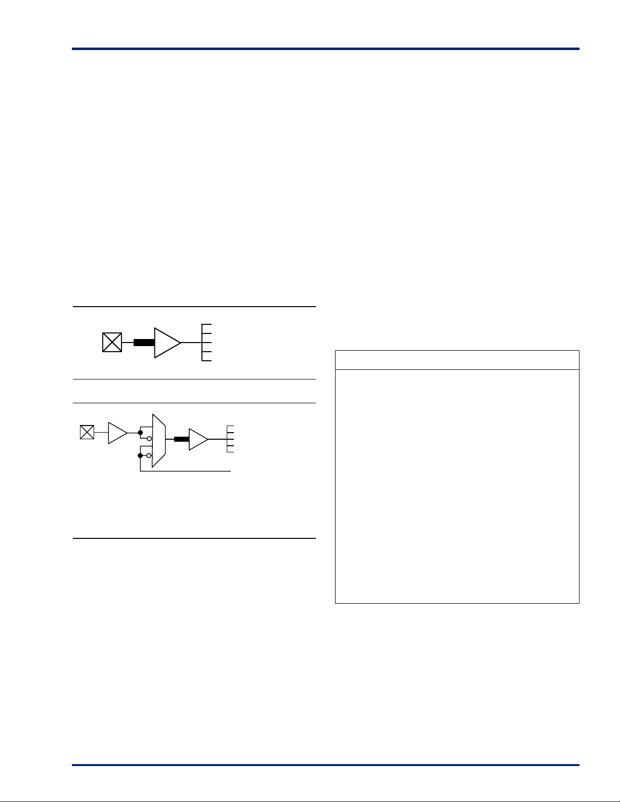
The R-cell contains a flip-flop featuring asynchronous clear,
asynchronous preset, and clock enable (using the S0 and S1
lines) control signals (Figure 1). The R-cell registers
feature programmable clock polarity selectable on a
register-by-register basis. This provides additional flexibility
while allowing mapping of synthesized functions into the eX
FPGA. The clock source for the R-cell can be chosen from
either the hard-wired clock or the routed clock.
Routed
Data Input
S0
The C-cell implements a range of combinatorial functions
up to 5 inputs (Figure 2). Inclusion of the DB input and its
associated inverter function dramatically increases the
number of combinatorial functions that can be
implemented in a single module from 800 options in
previous architectures to more than 4,000 in the eX
architecture.
Module Organization
Actel has arranged all C-cell and R-cell logic modules into
horizontal banks called Clusters. The eX devices contain
one type of Cluster, which contains two C-cells and one
R-cell.
To increase design efficiency and device performance, Actel
has further organized these modules into SuperClusters
(Figure 3 on page 4). The eX devices contain one type of
SuperClusters, which are two-wide groupings of one type of
clusters.
S1
Figure 1 • R-Cell
DirectConnect
Input
HCLK
CLKA,
CLKB,
Internal Logic
D0
D1
D2
D3
CKS
CKP
PSET
DQ
CLR
Sa
Y
Y
Sb
Figure 2 • C-Cell
DB
B1
A0 B0
v3.0 3
A1
Page 4
eX Family FPGAs
Routing Resources
Clusters and SuperClusters can be connected through the
use of two innovative local routing resources called
FastConnect and DirectConnect, which enable extremely
fast and predictable interconnection of modules within
Clusters and SuperClusters (Figure 4). This routing
architecture also dramatically reduces the number of
antifuses required to complete a circuit, ensuring the
highest possible performance.
DirectConnect is a horizontal routing resource that provides
connections from a C-cell to its neighboring R-cell in a given
SuperCluster. DirectConnect uses a hard-wired signal path
requiring no programmable interconnection to achieve its
fast signal propagation time of less than 0.1 ns (–P speed
grade).
R-Cell C-Cell
Routed
S1
Data Input
S0
PSET
DirectConnect
Input
FastConnect enables horizontal routing between any two
logic modules within a given SuperCluster and vertical
routing with the SuperCluster immediately below it. Only
one programmable connection is used in a FastConnect
path, delivering maximum pin-to-pin propagation of 0.3 ns
(–P speed grade).
In addition to DirectConnect and FastConnect, the
architecture makes use of two globally oriented routing
resources known as segmented routing and high-drive
routing. Actel’s segmented routing structure provides a
variety of track lengths for extremely fast routing between
SuperClusters. The exact combination of track lengths and
antifuses within each path is chosen by the 100 percent
automatic place-and-route software to minimize signal
propagation delays.
D0
D1
D2
YDQ
D3
Y
Sa Sb
HCLK
CLKA,
CLKB,
Internal Logic
CKS CKP
Figure 3 • Cluster Organization
Type 1 SuperClusters
CLR
DB
Cluster 1 Cluster 1
Type 1 SuperCluster
A0 B0 A1 B1
DirectConnect
• No antifuses
• 0.1 ns routing delay
FastConnect
• One antifuse
• 0.3 ns routing delay
Routing Segments
• Typically 2 antifuses
• Max. 5 antifuses
Figure 4 • DirectConnect and FastConnect for Type 1 SuperClusters
4v3.0
Page 5
eX Family FPGAs
Clock Resources
Actel’s high-drive routing structure provides three clock
networks. The first clock, called HCLK, is hardwired from
the HCLK buffer to the clock select MUX in each R-Cell.
HCLK cannot be connected to combinational logic. This
provides a fast propagation path for the clock signal,
enabling the 3.9ns clock-to-out (pad-to-pad) performance of
the eX devices. The hard-wired clock is tuned to provide a
clock skew of less than 0.1ns worst case.
The remaining two clocks (CLKA, CLKB) are global clocks
that can be sourced from external pins or from internal
logic signals within the eX device. CLKA and CLKB may be
connected to sequential cells or to combinational logic. If
CLKA or CLKB is sourced from internal logic signals then
the external clock pin cannot be used for any other input
and must be tied low or high. Figure 5 describes the clock
circuit used for the constant load HCLK. Figure 6 describes
the CLKA and CLKB circuit used in eX devices.
Constant Load
Clock Network
HCLKBUF
Figure 5 • eX HCLK Clock Pad
Clock Network
From Internal Logic
CLKBUF
CLKBUFI
CLKINT
CLKINTI
Figure 6 • eX Routed Clock Buffer
Other Architectural Features
Technology
Actel’s eX family is implemented on a high-voltage twin-well
CMOS process using 0.22
µ design rules. The metal-to-metal
antifuse is made up of a combination of amorphous silicon
and dielectric material with barrier metals and has an “on”
state resistance of 25
Ω with a capacitance of 1.0 fF for low
signal impedance.
Performance
The combination of architectural features described above
enables eX devices to operate with internal clock
frequencies exceeding 350 MHz for very fast execution of
complex logic functions. Thus, the eX family is an optimal
platform upon which to integrate the functionality
previously contained in CPLDs. In addition, designs that
previously would have required a gate array to meet
performance goals can now be integrated into an eX device
with dramatic improvements in cost and time to market.
Using timing-driven place-and-route tools, designers can
achieve highly deterministic device performance.
I/O Modules
Each I/O on an eX device can be configured as an input, an
output, a tristate output, or a bidirectional pin. Even without
the inclusion of dedicated I/O registers, these I/Os, in
combination with array registers, can achieve clock-to-out
(pad-to-pad) timing as fast as 3.9ns. I/O cells that have
embedded latches and flip-flops require instantiation in HDL
code; this is a design complication not encountered in eX
FPGAs. Fast pin-to-pin timing ensures that the device will
have little trouble interfacing with any other device in the
system, which in turn enables parallel design of system
components and reduces overall design time. See Table 1 for
more information.
Table 1 • I/O Features
Function Description
Input Buffer
Threshold
Selection
Flexible
Output
Driver
Output
Buffer
Power Up Individually selectable pull ups and pull
Hot Swapping
• TTL/3.3V LVTTL
• 2.5V LVCMOS 2
• 3.3V LVTTL
• 5.0V TTL/CMOS
“Hot-Swap” Capability
• I/O on an unpowered device does not
sink current
• Can be used for “cold sparing”
Selectable on an individual I/O basis
Individually selectable low-slew option
downs during power up (default is to power
up in tristate)
Enables deterministic power up of device
V
CCA
and V
can be powered in any order
CCI
eX I/Os are configured to be hot swappable. During power
up/down (or partial up/down), all I/Os are tristated. V
and V
do not have to be stable during power up/down,
CCI
CCA
and they do not require a specific power-up or power-down
sequence in order to avoid damage to the eX devices. After
the eX device is plugged into an electrically active system,
the device will not degrade the reliability of or cause
damage to the host system. The device’s output pins are
driven to a high impedance state until normal chip
v3.0 5
Page 6
eX Family FPGAs
operating conditions are reached. Please see the Actel SX-A
and RT54SX-S Devices in Hot-Swap and Cold-Sparing
Applications application note for more information on hot
swapping.
Power Requirements
The eX family supports mixed voltage operation and is
designed to tolerate 5.0V inputs in each case (Table 2).
Power consumption is extremely low due to the very short
distances signals, which are required to travel to complete a
circuit. Power requirements are further reduced because of
the small number of low-resistance antifuses in the path.
The antifuse architecture does not require active circuitry
to hold a charge (as do SRAM or EPROM), making it the
lowest-power architecture FPGA available today. Also, when
the device is in low power mode, the clock pins must not
float. They must be driven either HIGH or LOW. We
recommend that signals driving the clock pins be fixed at
HIGH or LOW rather than toggle to achieve maximum power
efficiency.
Table 2 • Supply Voltages
V
CCA
eX64
eX128
eX256
Low Power Mode
2.5V 2.5V 5.0V 2.5V
2.5V 3.3V 5.0V 3.3V
2.5V 5.0V 5.0V 5.0V
Maximum
V
CCI
Input
Tolerance
Maximum
Output
Drive
The new Actel eX family has been designed with a Low
Power Mode. This feature, activated with a special LP pin, is
particularly useful for battery-operated systems where
battery life is a primary concern. In this mode, the core of
the device is turned off and the device consumes minimal
power with low standby current. In addition, all input
buffers are turned off, and all outputs and bidirectional
buffers are tristated when the device enters this mode.
Since the core of the device is turned off, the states of the
registers are lost. The device must be re-initialized when
normal operating mode is achieved.
2.5V LP/Sleep Mode Specifications
Typical Conditions, V
Product Low Power Standby Current Units
eX64 100 µA
eX128 111 µA
eX256 134 µA
Boundary Scan Testing (BST)
CCA
, V
= 2.5V, TJ = 25° C
CCI
All eX devices are IEEE 1149.1 compliant. eX devices offer
superior diagnostic and testing capabilities by providing
Boundary Scan Testing (BST) and probing capabilities.
These functions are controlled through the special test pins
in conjunction with the program fuse. The functionality of
each pin is described in Table 3. In the dedicated test mode,
TCK, TDI, and TDO are dedicated pins and cannot be used
as regular I/Os. In flexible mode, TMS should be set HIGH
through a pull-up resistor of 10k
Ω. TMS can be pulled LOW
to initiate the test sequence.
Table 3 • Boundary Scan Pin Functionality
Program Fuse Blown
(Dedicated Test Mode)
TCK, TDI, TDO are
dedicated BST pins
No need for pull-up resistor
for TMS
Configuring Diagnostic Pins
Program Fuse Not Blown
(Flexible Mode)
TCK, TDI, TDO are flexible
and may be used as I/Os
Use a pull-up resistor of
10k
Ω on TMS
The JTAG and Probe pins (TDI, TCK, TMS, TDO, PRA, and
PRB) are placed in the desired mode by selecting the
appropriate check boxes in the “Variation” dialog window.
This dialog window is accessible through the Design Setup
Wizard under the Tools menu in Actel's Designer software.
TRST Pin
When the “Reserve JTAG Reset” box is checked, the TRST
pin will become a Boundary Scan Reset pin. In this mode,
the TRST pin will function as an asynchronous, active-low
input to initialize or reset the BST circuit. An internal
pull-up resistor will be automatically enabled on the TRST
pin.
The TRST pin will function as a user I/O when the “Reserve
JTAG Reset” box is not checked. The internal pull-up
resistor will be disabled in this mode.
Dedicated Test Mode
When the “Reserve JTAG” box is checked, the eX device is
placed in Dedicated Test mode, which configures the TDI,
TCK, and TDO pins for BST or in-circuit verification with
Silicon Explorer II. An internal pull-up resistor is
automatically enabled on both the TMS and TDI pins. In
Dedicated Test Mode, TCK, TDI, and TDO are dedicated test
pins and become unavailable for pin assignment in the Pin
Editor. The TMS pin will function as specified in the IEEE
1149.1 (JTAG) Specification.
Flexible Mode
When the “Reserve JTAG” box is not selected (default
setting in Designer software), eX is placed in Flexible mode,
which allows the TDI, TCK, and TDO pins to function as user
I/Os or BST pins. In this mode the internal pull-up resistors
on the TMS and TDI pins are disabled. An external 10k
pull-up resistor to V
is required on the TMS pin.
CCI
Ω
The TDI, TCK, and TDO pins are transformed from user I/Os
into BST pins when a rising edge on TCK is detected while
TMS is at logical low. Once the BST pins are in test mode
they will remain in BST mode until the internal BST state
6v3.0
Page 7
eX Family FPGAs
machine reaches the “logic reset” state. At this point the
BST pins will be released and will function as regular I/O
pins. The “logic reset” state is reached five TCK cycles after
the TMS pin is set to logical HIGH.
The Program fuse determines whether the device is in
Dedicated Test or Flexible mode. The default (fuse not
programmed) is Flexible mode.
Development Tool Support
The eX devices are fully supported by Actel’s line of FPGA
development tools, including the Actel Designer Series suite
and Libero, the FPGA design tool suite. Designer Series,
Actel’s suite of FPGA development tools for PCs and
Workstations, includes the ACTgen Macro Builder, timing
driven place-and-route, timing analysis tools, and fuse file
generation. Libero is a design management environment
that integrates the needed design tools, streamlines the
design flow, manages all design and log files, and passes
necessary design data between tools. Libero includes
Synplify, ViewDraw, Actel’s Designer Series, ModelSim HDL
Simulator, WaveFormer Lite, and Actel Silicon Explorer.
In addition, the eX devices contain internal probe circuitry
that provides built-in access to the output of every C-cell,
R-cell, and routed clock in the design, enabling 100-percent
real-time observation and analysis of a device's internal
logic nodes without design iteration. The probe circuitry is
accessed by Silicon Explorer II, an easy-to-use integrated
verification and logic analysis tool that can sample data at
100 MHz (asynchronous) or 66 MHz (synchronous). Silicon
Explorer II attaches to a PC’s standard COM port, turning
the PC into a fully functional 18-channel logic analyzer.
Silicon Explorer II allows designers to complete the design
verification process at their desks and reduces verification
time from several hours per cycle to only a few seconds.
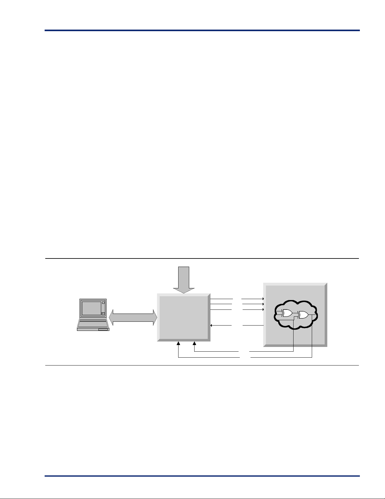
eX Probe Circuit Control Pins
The Silicon Explorer II tool uses the boundary scan ports
(TDI, TCK, TMS and TDO) to select the desired nets for
verification. The selected internal nets are assigned to the
PRA/PRB pins for observation. Figure 7 illustrates the
interconnection between Silicon Explorer II and the FPGA
to perform in-circuit verification. The TRST pin is equipped
with an internal pull-up resistor. To remove the boundary
scan state machine from the reset state during probing, it is
recommended that the TRST pin be left floating.
Design Considerations
For prototyping, the TDI, TCK, TDO, PRA, and PRB pins
should not be used as input or bidirectional ports. Because
these pins are active during probing, critical signals input
through these pins are not available while probing. In
addition, the Security Fuse should not be programmed
because doing so disables the probe circuitry.
Figure 7 • Probe Setup
Serial Connection
16
Channels
eX FPGA
TDI
TCK
TMS
Silicon Explorer II
TDO
PRA
PRB
v3.0 7
Page 8
eX Family FPGAs
2.5V/3.3V/5.0V Operating Conditions
Absolute Maximum Ratings
Symbol Parameter Limits Units
V
V
V
V
T
CCI
CCA
I
O
STG
DC Supply Voltage –0.3 to +6.0 V
DC Supply Voltage –0.3 to +3.0 V
Input Voltage –0.5 to +5.5 V
Output Voltage –0.5 to +V
Storage Temperature –65 to +150 °C
Note:
1. Stresses beyond those listed under “Absolute Maximum
Ratings” may cause permanent damage to the device. Exposure
1
+ 0.5 V
CCI
Recommended Operating Conditions
Parameter Commercial Industrial Units
Temperature
1
Range
2.5V Power Supply
Range (V
CCA, VCCI
3.3V Power Supply
Range (V
CCI
)
5.0V Power Supply
Range (V
CCI
)
0 to +70 –40 to +85 °C
2.3-2.7 2.3-2.7 V
)
3.0-3.6 3.0-3.6 V
4.75-5.25 4.5-5.5 V
Note:
1. Ambient temperature (TA).
to absolute maximum rated conditions for extended periods
may affect device reliability. Devices should not be operated
outside the Recommended Operating Conditions.
Typical eX Standby Current at 25°C
V
Product
V
CCA
CCI
= 2.5V
= 2.5V
V
CCA =
V
CCI
= 3.3V
eX64 397µA 497µA
eX128 696µA 795µA
eX256 698µA 796µA
2.5V
2.5V Electrical Specifications
Commercial Industrial
Symbol
V
OH
V
OL
V
IL
V
IH
I
OZ
1,2
tR, t
F
C
IO
3,4
I
CC
Parameter Min. Max. Min. Max. Units
V
= MIN, VI = V
DD
V
= MIN, VI = V
DD
V
= MIN, VI = V
DD
V
= MIN, VI = V
DD
V
= MIN, VI = V
DD
V
= MIN,VI = V
DD
Input Low Voltage, V
Input High Voltage, V
3-St ate Ou tput Le akage C ur rent, V
Input Transition Time tR, t
IH
IH
IH
IH
IH
IH
or V
or V
or V
or V
or V
or V
OUT
OUT
IL
IL
IL
IL
IL
IL
≤ V
VOL(max)
≥ V
F
VOH(min)
OUT
(I
= -100 µA) 2.1 2.1 V
OH
(I
= -1 mA) 2.0 2.0 V
OH
(I
= -2 mA) 1.7 1.7 V
OH
(IOL= 100µA) 0.2 0.2 V
(IOL= 1mA) 0.4 0.4 V
(IOL= 2 mA) 0.7 0.7 V
-0.3 0.7 -0.3 0.7 V
1.7 V
= V
or GND –10 10 –10 10 µA
CCI
I/O Capacitance 10 10 pF
Standby Current 1.0 3.0 mA
IV Curve5Can be derived from the IBIS model at www.actel.com/custsup/models/ibis.html.
Notes:
1. tR is the transition time from 0.7 V to 1.7V.
2. tF is the transition time from 1.7V to 0.7V.
3. ICC max Commercial –F = 5.0mA
4. ICC=I
CCI
+ I
CCA
+ 0.3 1.7 V
DD
+ 0.3 V
DD
10 10 ns
8v3.0
Page 9
eX Family FPGAs
3.3V Electrical Specifications
Commercial Industrial
Symbol Parameter
V
= MIN, VI = V
V
OH
V
OL
V
IL
V
IH
IIL/ I
I
OZ
tR, t
C
IO
I
CC
IH
F
3,4
DD
V
= MIN, VI = V
DD
V
= MIN, VI = V
DD
V
= MIN, VI = V
DD
Input Low Voltage 0.8 0.8 V
Input High Voltage 2.0 2.0 V
Input Leakage Current, VIN = V
3-State Output Leakage Current, V
1,2
Input Transition Time tR, t
I/O Capacitance 10 10 pF
Standby Current 1.5 10 mA
IH
IH
IH
IH
or V
or V
or V
or V
(I
IL
IL
IL
IL
or GND –10 10 –10 10 µA
CCI
= V
OUT
F
or GND –10 10 –10 10 µA
CCI
= -1mA) 0. 9 V
OH
(I
= -8mA) 2.4 2.4 V
OH
(IOL= 1mA) 0.1 V
(IOL= 12mA) 0.4 0.4 V
Min. Max. Min. Max. Units
CCI
IV Curve5Can be derived from the IBIS model at www.actel.com/custsup/models/ibis.html.
Notes:
1. tR is the transition time from 0.8 V to 2.0V.
2. tF is the transition time from 2.0V to 0.8V.
3. ICC max Commercial –F=5.0mA
4. ICC=I
CCI
+ I
CCA
5.0V Electrical Specifications
Commercial Industrial
0.9 V
CCI
CCI
0.1 V
CCI
10 10 ns
V
V
Symbol Parameter
V
= MIN, VI = V
V
OH
V
OL
V
IL
V
IH
IIL/ I
I
OZ
tR, t
C
IO
I
CC
IH
F
3,4
DD
V
= MIN, VI = V
DD
V
= MIN, VI = V
DD
V
= MIN, VI = V
DD
Input Low Voltage 0.8 0.8 V
Input High Voltage 2.0 2.0 V
Input Leakage Current, VIN = V
3-State Output Leakage Current, V
1,2
Input Transition Time tR, t
I/O Capacitance 10 10 pF
Standby Current 15 20 mA
IH
IH
IH
IH
or V
or V
or V
or V
(I
IL
IL
IL
IL
or GND –10 10 –10 10 µA
CCI
= V
OUT
F
or GND –10 10 –10 10 µA
CCI
= -1mA) 0. 9 V
OH
(I
= -8mA) 2.4 2.4 V
OH
(IOL= 1mA) 0.1 V
(IOL= 12mA) 0.4 0.4 V
Min. Max. Min. Max. Units
CCI
IV Curve5Can be derived from the IBIS model at www.actel.com/custsup/models/ibis.html
Notes:
1. tR is the transition time from 0.8 V to 2.0V.
2. tF is the transition time from 2.0V to 0.8V.
3. ICC max Commercial –F=20mA
4. ICC=I
CCI
+ I
CCA
0.9 V
CCI
CCI
0.1 V
CCI
10 10 ns
V
V
v3.0 9
Page 10
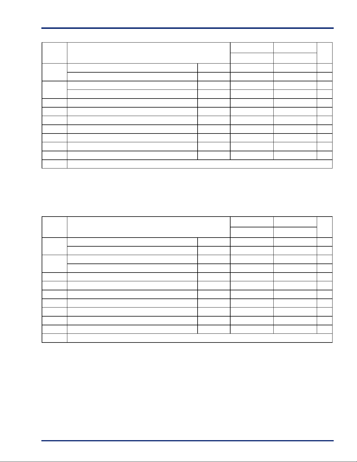
eX Dynamic Power Consumption – High Frequency
300
250
200
150
100
Power (mW)
50
0
50 100 150 200
Frequency (MHz)
Notes:
1. Device filled with 16-bit counters.
2. V
CCA
, V
= 2.7V, device tested at room temperature.
CCI
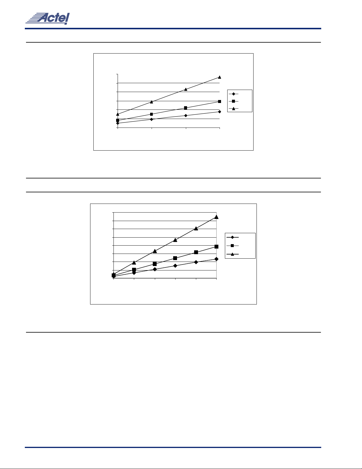
eX Dynamic Power Consumption – Low Frequency
eX Family FPGAs
eX 64
eX 128
eX 256
Notes:
1. Device filled with 16-bit counters.
2. V
CCA
, V
= 2.7V, device tested at room temperature.
CCI
80
70
60
50
40
30
Power (mW)
20
10
0
0 1020304050
Frequency (MH z)
eX64
eX128
eX256
10 v3.0
Page 11
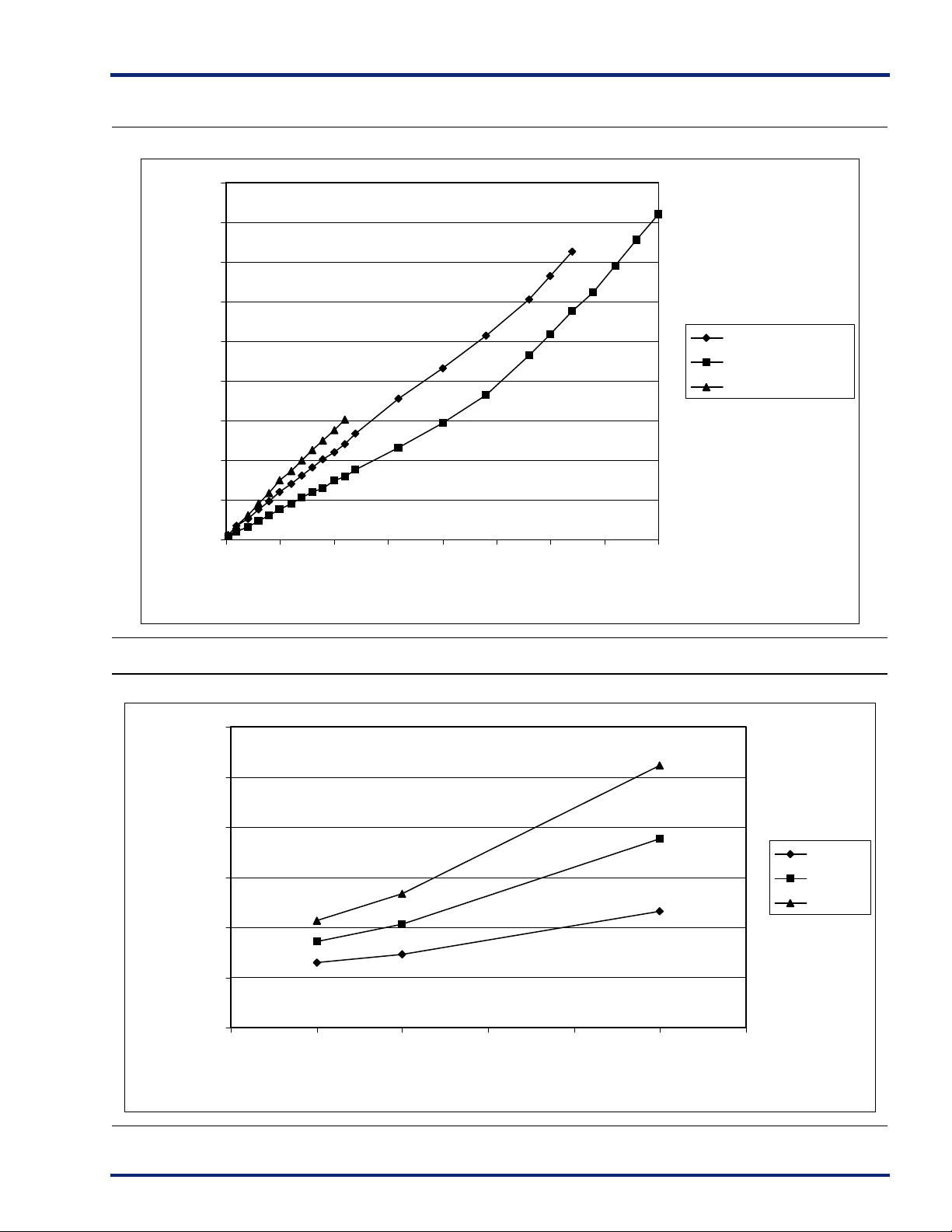
eX Family FPGAs
Total Dynamic Power (mW)
180
160
140
120
100
80
60
40
Total Dynamic Power (mW)
20
0
0 25 50 75 100 125 150 175 200
Freque nc y (MHz)
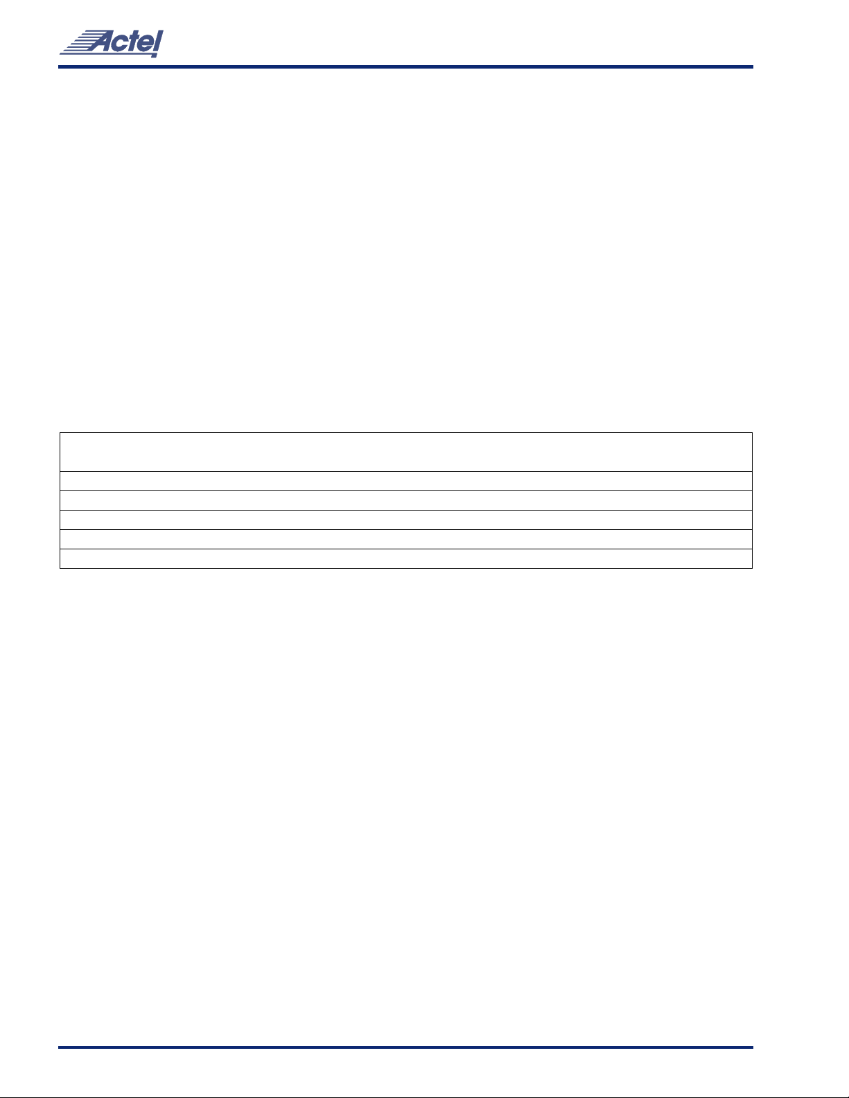
System Power at 5%, 10%, and 15% Duty Cycle
12,000
10,000
32-bit Dec ode r
8 x 8-bi t Count e rs
SDRAM Controller
8,000
6,000
4,000
System Power (uW)
2,000
0
5% DC
10% DC
15% DC
0 102030405060
Freque ncy ( M Hz)
v3.0 11
Page 12
Junction Temperature (TJ)
The temperature variable in the Designer Series software
refers to the junction temperature, not the ambient
temperature. This is an important distinction because the
heat generated from dynamic power consumption is usually
hotter than the ambient temperature. Equation 1, shown
below, can be used to calculate junction temperature.
Junction Temperature =
∆T + T
a
(1)
Where:
= Ambient Temperature
T
a
∆T = Temperature gradient between junction (silicon) and
ambient
∆T = θ
ja
* P
P = Power
eX Family FPGAs
θ
= Junction to ambient of package. θja numbers are
ja
located in the Package Thermal Characteristics section
below.
Package Thermal Characteristics
The device junction to case thermal characteristic is θjc,
θ
and the junction to ambient air characteristic is
thermal characteristics for
θ
are shown with two different
ja
. The
ja
air flow rates.
The maximum junction temperature is 150
°C.
A sample calculation of the absolute maximum power
dissipation allowed for a TQFP 100-pin package at
commercial temperature and still air is as follows:
Max. junction temp. (°C) Max. ambient temp. (°C)–
Maximum Power Allowed
Package Type Pin Count θ
Thin Quad Flat Pack (TQFP) 64 14 51.2 35 °C/W
Thin Quad Flat Pack (TQFP) 100 12 37.5 30 °C/W
Chip Scale Package (CSP) 49 3 71.3 56.0 °C/W
Chip Scale Package (CSP) 128 3 54.1 47.8 °C/W
Chip Scale Package (CSP) 180 3 57.8 51 °C/W
---------------------------------------------------------------------------------------------------------------------------------
θ
ja
(° C/W)
jc
150° C70°C–
-----------------------------------
37.5°C/W
θ
ja
Still Air
2.1W===
θ
ja
300 ft/min Units
12 v3.0
Page 13

eX Family FPGAs
eX Timing Model*
Routed
Clock
Input Delays Internal Delays Predicted
I/O Module
t
INYH
t
RCKH
(100% Load)
I/O Module
t
INYH
= 0.7 ns
= 1.3 ns
= 0.7 ns
t
IRD1
t
IRD2
t
IRD1
t
t
t
t
SUD
HD
SUD
HD
= 0.0 ns
= 0.3 ns
= 0.4 ns
= 0.5 ns
= 0.0 ns
= 0.3 ns
= 0.5ns
Combinatorial
Cell
t
= 0.7 ns
PD
Register
Cell
DQ
t
= 0.6 ns
RCO
Register
Cell
DQ
t
RD1
t
RD1
t
RD1
t
RD4
t
RD8
= 0.3 ns
= 0.3 ns
Routing
Delays
= 0.3 ns
= 0.7 ns
= 1.2 ns
Output Delays
I/O Module
I/O Module
t
ENZL
t
= 2.6 ns
DHL
I/O Module
t
ENZL
t
= 2.6 ns
DHL
t
DHL
= 1.9 ns
= 1.9 ns
= 2.6 ns
Hard-Wired
Clock
t
HCKH
= 1.1 ns
t
RCO
= 0.6 ns
*Values shown for eX128–P, worst-case commercial conditions (5.0V, 35pF Pad Load).
Hard-Wired Clock
External Setup = t
INYH
+ t
IRD1
+ t
SUD
– t
HCKH
Routed Clock
External Setup = t
= 0.7 + 0.3 + 0.5 – 1.1 = 0.4 ns
Clock-to-Out (Pad-to-Pad), typical
+ t
=t
HCKH
RCO
+ t
RD1
+ t
DHL
Clock-to-Out (Pad-to-Pad), typical
= 1.1 + 0.6 + 0.3 + 2.6 = 4.6 ns
INYH
+ t
IRD2
+ t
SUD
– t
RCKH
= 0.7 + 0.4 + 0.5 – 1.3= 0.3 ns
+ t
+ t
=t
RCKH
RCO
RD1
+ t
DHL
= 1.3+ 0.6 + 0.3 + 2.6 = 4.8 ns
v3.0 13
Page 14

Output Buffer Delays
eX Family FPGAs
E
V
CC
In
Out
V
OL
50%
t
DLH
50%
V
OH
1.5V
AC Test Loads
Load 1
(Used to measure
propagati o n dela y)
To the output
under test
t
DHL
35 pF
GND
1.5V
D
En
Out
TRIBUFF
V
CC
50%
V
CC
1.5V
t
ENZL
50%
V
OL
PAD
t
ENLZ
Load 2
(Used to measure enable delays)
V
CC
GND
R to VCC for t
To the output
under test
R to GND for t
R = 1 kΩ
To AC test loads (shown below)
GND
10%
En
Out
50%
GND
t
ENZH
(Used to measure disable delays)
V
PZL
PZH
To the output
under test
V
CC
Load 3
CC
50%
V
OH
1.5V
GND
R to VCC for t
R to GND for t
R = 1 kΩ
t
ENHZ
GND
90%
PLZ
PHZ
35 pF
Input Buffer Delays C-Cell Delays
Y
0V
50%
S, A or B
Out
GND
Out
50%
t
In
Out
GND
PAD
1.5V
INBUF
3V
1.5V
V
CC
50%
S
A
Y
B
V
CC
t
PD
GND
t
PD
GND
50%
50%
V
CC
50%
PD
50% 50%
t
PD
5 pF
V
CC
14 v3.0
Page 15

eX Family FPGAs
Cell Timing Characteristics
Flip-Flops
D
PRESET
Q
CLK
(Positive edge triggered)
D
t
HPWH
t
RPWH
,
CLK
CLR
PRESET
t
SUD
Q
Timing Characteristics
Timing characteristics for eX devices fall into three
categories: family-dependent, device-dependent, and
design-dependent. The input and output buffer
characteristics are common to all eX family members.
Internal routing delays are device-dependent. Design
dependency means actual delays are not determined until
after placement and routing of the user’s design are
complete. Delay values may then be determined by using
the Timer utility or performing simulation with post-layout
delays.
Critical Nets and Typical Nets
Propagation delays are expressed only for typical nets,
which are used for initial design performance evaluation.
Critical net delays can then be applied to the most timing
critical paths. Critical nets are determined by net property
assignment prior to placement and routing. Up to
six percent of the nets in a design may be designated as
critical.
CLR
t
HD
t
HP
t
,
HPWL
t
RCO
Long Tracks
t
RPWL
t
CLR
t
WASYN
t
PRESET
Some nets in the design use long tracks. Long tracks are
special routing resources that span multiple rows, columns,
or modules. Long tracks employ three to five antifuse
connections. This increases capacitance and resistance,
resulting in longer net delays for macros connected to long
tracks. Typically, no more than six percent of nets in a fully
utilized device require long tracks. Long tracks contribute
approximately 4 ns to 8.4 ns delay. This additional delay is
represented statistically in higher fanout routing delays.
Timing Derating
eX devices are manufactured with a CMOS process.
Therefore, device performance varies according to
temperature, voltage, and process changes. Minimum
timing parameters reflect maximum operating voltage,
minimum operating temperature, and best-case processing.
Maximum timing parameters reflect minimum operating
voltage, maximum operating temperature, and worst-case
processing.
Temperature and Voltage Derating Factors
(Normalized to Worst-Case Commercial, TJ = 70° C, V
Junction Temperature (TJ)
V
CCA
2.3
2.5
2.7
–55 –40 0 25 70 85 125
0.75 0.79 0.88 0.89 1.00 1.04 1.16
0.70 0.74 0.82 0.83 0.93 0.97 1.08
0.66 0.69 0.79 0.79 0.88 0.92 1.02
v3.0 15
CCA
= 2.3V)
Page 16

eX Family Timing Characteristics
eX Family FPGAs
(Worst-Case Commercial Conditions, V
= 2.3V, TJ = 70°C)
CCA
‘–P’ Speed ‘Std’ Speed ‘–F’ Speed
Parameter Description Min. Max. Min. Max. Min. Max. Units
C-Cell Propagation Delays
t
PD
Internal Array Module 0.7 1.0 1.4 ns
Predicted Routing Delays
t
DC
t
FC
t
RD1
t
RD2
t
RD3
t
RD4
t
RD8
t
RD12
FO=1 Routing Delay, DirectConnect 0.1 0.1 0.2 ns
FO=1 Routing Delay, FastConnect 0.3 0.5 0.7 ns
FO=1 Routing Delay 0.3 0.5 0.7 ns
FO=2 Routing Delay 0.4 0.6 0.8 ns
FO=3 Routing Delay 0.5 0.8 1.1 ns
FO=4 Routing Delay 0.7 1.0 1.3 ns
FO=8 Routing Delay 1.2 1.7 2.4 ns
FO=1 2 Routing Delay 1.7 2.5 3.5 ns
1
2
R-Cell Timing
t
RCO
t
CLR
t
PRESET
t
SUD
t
HD
t
WASYN
t
RECASYN
t
HASYN
Sequential Clock-to-Q 0.6 0.9 1.3 ns
Asynchronous Clear-to-Q 0.6 0.8 1.2 ns
Asynchronous Preset-to-Q 0.7 0.9 1.3 ns
Flip-Flop Data Input Set-Up 0.5 0.7 1.0 ns
Flip-Flop Data Input Hold 0.0 0.0 0.0 ns
Asynchronous Pulse Width 1.3 1.9 2.6 ns
Asynchronous Recovery Time 0.3 0.5 0.7 ns
Asynchronous Hold Time 0.3 0.5 0.7 ns
2.5V Input Module Propagation Delays
t
INYH
t
INYL
Input Data Pad-to-Y HIGH 0.6 0.9 1.3 ns
Input Data Pad-to-Y LOW 0.8 1.1 1.5 ns
3.3V Input Module Propagation Delays
t
INYH
t
INYL
Input Data Pad-to-Y HIGH 0.7 1.0 1.4 ns
Input Data Pad-to-Y LOW 0.9 1.3 1.8 ns
5.0V Input Module Propagation Delays
t
INYH
t
INYL
Input Module Predicted Routing Delays
t
IRD1
t
IRD2
t
IRD3
t
IRD4
t
IRD8
t
IRD12
Input Data Pad-to-Y HIGH 0.7 1.0 1.4 ns
Input Data Pad-to-Y LOW 0.9 1.3 1.8 ns
2
FO=1 Routing Delay 0.3 0.4 0.5 ns
FO=2 Routing Delay 0.4 0.6 0.8 ns
FO=3 Routing Delay 0.5 0.8 1.1 ns
FO=4 Routing Delay 0.7 1.0 1.3 ns
FO=8 Routing Delay 1.2 1.7 2.4 ns
FO=1 2 Routing Delay 1.7 2.5 3.5 ns
Notes:
1. For dual-module macros, use tPD + t
RD1
+ t
PDn
, t
+ t
+ t
or t
+ t
+ t
RCO
RD1
PDn
PD1
RD1
, whichever is appropriate.
SUD
2. Routing delays are for typical designs across worst-case operating conditions. These parameters should be used for estimating device
performance. Post-route timing analysis or simulation is required to determine actual worst-case performance.
16 v3.0
Page 17

eX Family FPGAs
eX Family Timing Characteristics (Continued)
(Worst-Case Commercial Conditions V
CCA
= 2.3V, V
= 4.75V, TJ = 70°C)
CCI
‘–P’ Speed ‘Std’ Speed ‘–F’ Speed
Parameter Description Min. Max. Min. Max. Min. Max. Units
Dedicated (Hard-Wired) Array Clock Networks
t
HCKH
Input LOW to HIGH
(Pad to R-Cell Input) 1.1 1.6 2.3 ns
t
HCKL
Input HIGH to LOW
(Pad to R-Cell Input) 1.1 1.6 2.3 ns
t
HPWH
t
HPWL
t
HCKSW
t
HP
f
HMAX
Minimum Pulse Width HIGH 1.4 2.0 2.8 ns
Minimum Pulse Width LOW 1.4 2.0 2.8 ns
Maximum Skew <0.1 <0.1 <0.1 ns
Minimum Period 2.8 4.0 5.6 ns
Maximum Frequency 357 250 178 MHz
Routed Array Clock Networks
t
RCKH
Input LOW to HIGH (Light Load)
(Pad to R-Cell Input) MAX. 1.1 1.6 2.2 ns
t
RCKL
Input HIGH to LOW (Light Load)
(Pad to R-Cell Input) MAX. 1.0 1.4 2.0 ns
t
RCKH
Input LOW to HIGH (50% Load)
(Pad to R-Cell Input) MAX. 1.2 1.7 2.4 ns
t
RCKL
Input HIGH to LOW (50% Load)
(Pad to R-Cell Input) MAX. 1.2 1.7 2.4 ns
t
RCKH
Input LOW to HIGH (100% Load)
(Pad to R-Cell Input) MAX. 1.3 1.9 2.6 ns
t
RCKL
Input HIGH to LOW (100% Load)
(Pad to R-Cell Input) MAX. 1.3 1.9 2.6 ns
t
RPWH
t
RPWL
t
RCKSW
t
RCKSW
t
RCKSW
1
1
1
Min. Pulse Width HIGH 1.5 2.1 3.0 ns
Min. Pulse Width LOW 1.5 2.1 3.0 ns
Maximum Skew (Light Load) 0.2 0.3 0.4 ns
Maximum Skew (50% Load) 0.1 0.2 0.3 ns
Maximum Skew (100% Load) 0.1 0.1 0.2 ns
Note:
1. Clock skew improves as the clock network becomes more heavily loaded.
v3.0 17
Page 18

eX Family Timing Characteristics (Continued)
eX Family FPGAs
(Worst-Case Commercial Conditions V
CCA
= 2.3V, V
= 2.3V or 3.0V, TJ = 70°C)
CCI
‘–P’ Speed ‘Std’ Speed ‘–F’ Speed
Parameter Description Min. Max. Min. Max. Min. Max. Units
Dedicated (Hard-Wired) Array Clock Networks
t
HCKH
t
HCKL
t
HPWH
t
HPWL
t
HCKSW
t
HP
f
HMAX
Input LOW to HIGH
(Pad to R-Cell Input)
Input HIGH to LOW
(Pad to R-Cell Input)
1.1 1.6 2.3
1.1 1.6 2.3
ns
ns
Minimum Pulse Width HIGH 1.4 2.0 2.8 ns
Minimum Pulse Width LOW 1.4 2.0 2.8 ns
Maximum Skew <0.1 <0.1 <0.1 ns
Minimum Period 2.8 4.0 5.6 ns
Maximum Frequency 357 250 178 MHz
Routed Array Clock Networks
t
RCKH
t
RCKL
t
RCKH
t
RCKL
t
RCKH
t
RCKL
t
RPWH
t
RPWL
t
RCKSW
t
RCKSW
t
RCKSW
1
1
1
Input LOW to HIGH (Light Load)
(Pad to R-Cell Input) MAX.
Input HIGH to LOW (Light Load)
(Pad to R-Cell Input) MAX.
Input LOW to HIGH (50% Load)
(Pad to R-Cell Input) MAX.
Input HIGH to LOW (50% Load)
(Pad to R-Cell Input) MAX.
Input LOW to HIGH (100% Load)
(Pad to R-Cell Input) MAX.
Input HIGH to LOW (100% Load)
(Pad to R-Cell Input) MAX.
1.0 1.4 2.0
1.0 1.4 2.0
1.2 1.7 2.4
1.2 1.7 2.4
1.4 2.0 2.8
1.4 2.0 2.8
ns
ns
ns
ns
ns
ns
Min. Pulse Width HIGH 1.4 2.0 2.8 ns
Min. Pulse Width LOW 1.4 2.0 2.8 ns
Maximum Skew (Light Load) 0.2 0.3 0.4 ns
Maximum Skew (50% Load) 0.2 0.2 0.3 ns
Maximum Skew (100% Load) 0.1 0.1 0.2 ns
Note:
1. Clock skew improves as the clock network becomes more heavily loaded.
18 v3.0
Page 19

eX Family FPGAs
eX Family Timing Characteristics (Continued)
(Worst-Case Commercial Conditions V
= 2.3V, TJ = 70°C)
CCA
‘–P’ Speed ‘Std’ Speed ‘–F’ Speed
Parameter Description Min. Max. Min. M ax. Min. Max. Units
2.5V LVTTL Output Module Timing1 (V
t
DLH
t
DHL
t
DHLS
t
ENZL
t
ENZLS
t
ENZH
t
ENLZ
t
ENHZ
d
TLH
d
THL
d
THLS
Data-to-Pad LOW to HIGH 3.3 4.7 6.6 ns
Data-to-Pad HIGH to LOW 3.5 5.0 7.0 ns
Data-to-Pad HIGH to LOW—Low Slew 11.6 16.6 23.2 ns
Enable-to-Pad, Z to L 2.5 3.6 5.1 ns
Enable-to-Pad Z to L—Low Slew 11.8 16.9 23.7 ns
Enable-to-Pad, Z to H 3.4 4.9 6.9 ns
Enable-to-Pad, L to Z 2.1 3.0 4.2 ns
Enable-to-Pad, H to Z 2.4 5.67 7.94 ns
Delta Delay vs. Load LOW to HIGH 0.034 0.046 0.066 ns/pF
Delta Delay vs. Load HIGH to LOW 0.016 0.022 0.05 ns/pF
Delta Delay vs. Load HIGH to LOW—Low
Slew
3.3V LVTTL Output Module Timing1 (V
t
DLH
t
DHL
t
DHLS
t
ENZL
t
ENZLS
t
ENZH
t
ENLZ
t
ENHZ
d
TLH
d
THL
d
THLS
Data-to-Pad LOW to HIGH 2.8 4.0 5.6 ns
Data-to-Pad HIGH to LOW 2.7 3.9 5.4 ns
Data-to-Pad HIGH to LOW—Low Slew 9.7 13.9 19.5 ns
Enable-to-Pad, Z to L 2.2 3.2 4.4 ns
Enable-to-Pad Z to L—Low Slew 9.7 13.9 19.6 ns
Enable-to-Pad, Z to H 2.8 4.0 5.6 ns
Enable-to-Pad, L to Z 2.8 4.0 5.6 ns
Enable-to-Pad, H to Z 2.6 3.8 5.3 ns
Delta Delay vs. Load LOW to HIGH 0.02 0.03 0.046 ns/pF
Delta Delay vs. Load HIGH to LOW 0.016 0.022 0.05 ns/pF
Delta Delay vs. Load HIGH to LOW—Low
Slew
5.0V TTL Output Mo dul e Tim i n g1 (V
t
DLH
t
DHL
t
DHLS
t
ENZL
t
ENZLS
t
ENZH
t
ENLZ
Data-to-Pad LOW to HIGH 2.0 2.9 4.0 ns
Data-to-Pad HIGH to LOW 2.6 3.7 5.2 ns
Data-to-Pad HIGH to LOW—Low Slew 6.8 9.7 13.6 ns
Enable-to-Pad, Z to L 1.9 2.7 3.8 ns
Enable-to-Pad Z to L—Low Slew 6.8 9.8 13.7 ns
Enable-to-Pad, Z to H 2.1 3.0 4.1 ns
Enable-to-Pad, L to Z 3.3 4.8 6.6 ns
CCI
CCI
CCI
= 2.3V)
0.05 0.072 0.1 ns/pF
= 3.0V)
0.05 0.072 0.1 ns/pF
= 4.75V)
Note:
1. Delays based on 35 pF loading.
v3.0 19
Page 20

Pin Description
eX Family FPGAs
CLKA/B Clock A and B
These pins are clock inputs for clock distribution networks.
Input levels are compatible with standard TTL or LVTTL
specifications. The clock input is buffered prior to clocking
the R-cells. If not used, this pin must be set LOW or HIGH on
the board. It must not be left floating.
GND Ground
LOW supply voltage.
HCLK Dedicated (Hard-wired)
Array Clock
This pin is the clock input for sequential modules. Input
levels are compatible with standard TTL or LVTTL
specifications. This input is directly wired to each R-cell and
offers clock speeds independent of the number of R-cells
being driven. If not used, this pin must be set LOW or HIGH
on the board. It must not be left floating.
I/O Input/Output
The I/O pin functions as an input, output, tristate, or
bidirectional buffer. Based on certain configurations, input
and output levels are compatible with standard TTL or
LVTTL specifications. Unused I/O pins are automatically
tristated by the Designer Series software.
LP Low Power Pin
Controls the low power mode of the eX devices. The device
is placed in the low power mode by connecting the LP pin
to logic high. In low power mode, all I/Os are tristated, all
input buffers are turned OFF, and the core of the devices is
turned OFF. To exit the low power mode, the LP pin must
be set LOW. The device enters the low power mode 800ns
after the LP pin is driven to a logic HIGH. It will resume
normal operation in 200
µs after the LP pin is driven to a
logic low. The logic high level on the LP pin must never
exceed the V
NC No Connection
voltage. Refer to the VSV pin description.
SV
This pin is not connected to circuitry within the device.
These pins can be driven to any voltage or can be left
floating with no effect on the operation of the device.
PRA, I/O
PRB, I/O Probe A/B
The Probe pin is used to output data from any user-defined
design node within the device. This independent diagnostic
pin can be used in conjunction with the other probe pin to
allow real-time diagnostic output of any signal path within
the device. The Probe pin can be used as a user-defined I/O
when verification has been completed. The pin’s probe
capabilities can be permanently disabled to protect
programmed design confidentiality.
TCK, I/O Test Clock
Test clock input for diagnostic probe and device
programming. In flexible mode, TCK becomes active when
the TMS pin is set LOW (refer to Table 3 on page 6). This pin
functions as an I/O when the boundary scan state machine
reaches the “logic reset” state.
TDI, I/O Test Data Input
Serial input for boundary scan testing and diagnostic probe.
In flexible mode, TDI is active when the TMS pin is set LOW
(refer to Table 3 on page 6). This pin functions as an I/O
when the boundary scan state machine reaches the “logic
reset” state.
TDO, I/O Test Data Output
Serial output for boundary scan testing. In flexible mode,
TDO is active when the TMS pin is set LOW (refer to Table 3
on page 6). This pin functions as an I/O when the boundary
scan state machine reaches the "logic reset" state. When
Silicon Explorer is being used, TDO will act as an output
when the "checksum" command is run. It will return to user
IO when "checksum" is complete.
TMS Test Mode Select
The TMS pin controls the use of the IEEE 1149.1 Boundary
Scan pins (TCK, TDI, TDO, TRST). In flexible mode when
the TMS pin is set LOW, the TCK, TDI, and TDO pins are
boundary scan pins (refer to Table 3 on page 6). Once the
boundary scan pins are in test mode, they will remain in that
mode until the internal boundary scan state machine
reaches the “logic reset” state. At this point, the boundary
scan pins will be released and will function as regular I/O
pins. The “logic reset” state is reached 5 TCK cycles after
the TMS pin is set HIGH. In dedicated test mode, TMS
functions as specified in the IEEE 1149.1 specifications.
TRST, I/O Boundary Scan Reset Pin
Once it is configured as the JTAG Reset pin, the TRST pin
functions as an active-low input to asynchronously initialize
or reset the boundary scan circuit. The TRST pin is equipped
with an internal pull-up resistor. This pin functions as an I/O
when the “Reserve JTAG Reset Pin” is not selected in
Designer.
V
CCI
Supply Voltage
Supply voltage for I/Os. See Table 2 on page 6.
V
CCA
Supply Voltage
Supply voltage for Array. See Table 2 on page 6.
V
SV
Programming Voltage
Supply voltage used for device programming. This pin can be
tied to V
fuse is programmed, the V
CCA
or V
but cannot exceed 3.6V. If the security
CCI
limit is extended to 6.0V.
SV
20 v3.0
Page 21

eX Family FPGAs
Package Pin Assignments
64-Pin TQFP (Top View)
64
1
64-Pin
TQFP
v3.0 21
Page 22

64-Pin TQFP
Pin Number
1
eX64
Function
GND GND 33 GND GND
eX128
Function Pin Number
2 TDI, I/O TDI, I/O 34 I/O I/O
3
4
5
6 V
I/O I/O
TMS TMS
GND GND
CCI
V
CCI
7 I/O I/O 39 I/O I/O
8
9
I/O I/O
NC I/O
10 NC I/O 42 I/O I/O
11 TRST, I/O TRST, I/O 43 I/O I/O
12 I/O I/O 44 V
13
14
NC I/O
GND GND
15 I/O I/O 47 I/O I/O
16 I/O I/O 48 I/O I/O
17
18
19 V
I/O I/O
I/O I/O
CCI
V
CCI
20 I/O I/O 52 V
21 PRB, I/O PRB, I/O 53 I/O I/O
22
23
V
CCA
V
CCA
GND GND
24 I/O I/O 56 CLKB CLKB
25 HCLK HCLK 57 V
26
27
I/O I/O
I/O I/O
28 I/O I/O 60 I/O I/O
29 I/O I/O 61 V
30 I/O I/O 62 I/O I/O
31
32
I/O I/O
TDO, I/O TDO, I/O
1. Please read the VSV and LP pin descriptions for restrictions on their use.
eX Family FPGAs
35
36
37
eX64
Function
I/O I/O
1
V
SV
V
CCI
eX128
Function
V
SV
V
CCI
38 I/O I/O
40
41
45
46
49
50
NC I/O
NC I/O
CCA
GND/LP
1
GND/ LP
GND GND
I/O I/O
I/O I/O
V
CCA
51 I/O I/O
V
V
V
CCI
CCA
CCI
54
55
58
59
63
64
CCI
I/O I/O
CLKA CLKA
CCA
GND GND
PRA, I/O PRA, I/O
CCI
I/O I/O
TCK, I/O TCK, I/O
1
1
22 v3.0
Page 23

eX Family FPGAs
Package Pin Assignments (Continued)
100-Pin TQFP (Top View)
100
1
100-Pin
TQFP
v3.0 23
Page 24

eX Family FPGAs
100-TQFP
Pin Number
eX64
Function
eX128
Function
eX256
Function Pin Number
eX64
Function
eX128
Function
1 GND GND GND 51 GND GND GND
2 TDI, I/O TDI, I/O TDI, I/O 52 NC NC I/O
3 NC NC I/O 53 NC NC I/O
4 NC NC I/O 54 NC NC I/O
5 NC NC I/O 55 I/O I/O I/O
6 I/O I/O I/O 56 I/O I/O I/O
7 TMS TMS TMS 57
8V
CCI
V
CCI
V
CCI
58 V
1
V
SV
CCI
1
V
SV
V
CCI
9 GND GND GND 59 NC I/O I/O
10 NC I/O I/O 60 I/O I/O I/O
11 NC I/O I/O 61 NC I/O I/O
12 I/O I/O I/O 62 I/O I/O I/O
13 NC I/O I/O 63 NC I/O I/O
14 I/O I/O I/O 64 I/O I/O I/O
15 NC I/O I/O 65 NC I/O I/O
16 TRST, I/O TRST, I/O TRST, I/O 66 I/O I/O I/O
17 NC I/O I/O 67 V
CCA
18 I/O I/O I/O 68 GND/LP
1
V
CCA
GND/LP
19 NC I/O I/O 69 GND GND GND
20 V
CCI
V
CCI
V
CCI
70 I/O I/O I/O
21 I/O I/O I/O 71 I/O I/O I/O
22 NC I/O I/O 72 NC I/O I/O
23 NC NC I/O 73 NC NC I/O
24 NC NC I/O 74 NC NC I/O
25 I/O I/O I/O 75 NC NC I/O
26 I/O I/O I/O 76 NC I/O I/O
27 I/O I/O I/O 77 I/O I/O I/O
28 I/O I/O I/O 78 I/O I/O I/O
29 I/O I/O I/O 79 I/O I/O I/O
30 I/O I/O I/O 80 I/O I/O I/O
31 I/O I/O I/O 81 I/O I/O I/O
32 I/O I/O I/O 82
33 I/O I/O I/O 83
34 PRB, I/O PRB, I/O PRB, I/O 84
35 V
CCA
V
CCA
V
CCA
85
36 GND GND GND 86
37 NC NC NC 87
38 I/O I/O I/O 88
39 HCLK HCLK HCLK 89
40 I/O I/O I/O 90
41 I/O I/O I/O 91
42 I/O I/O I/O 92
43 I/O I/O I/O 93
44 V
CCI
V
CCI
V
CCI
94
45 I/O I/O I/O 95
46 I/O I/O I/O 96
47 I/O I/O I/O 97
48 I/O I/O I/O 98
49 TDO, I/O TDO, I/O TDO, I/O 99
50 NC I/O I/O 100
V
CCI
V
CCI
I/O I/O
I/O I/O
I/O I/O
I/O I/O
CLKA CLKA
CLKB CLKB
NC NC
V
CCA
V
CCA
GND GND
PRA, I/O PRA, I/O
I/O I/O
I/O I/O
I/O I/O
I/O I/O
I/O I/O
I/O I/O
I/O I/O
TCK, I/O TCK, I/O
1. Please read the VSV and LP pin descriptions for restrictions on their use.
eX256
Function
1
V
SV
V
CCI
V
1
CCA
GND/LP
V
CCI
1
I/O
I/O
I/O
I/O
CLKA
CLKB
NC
V
CCA
GND
PRA, I/O
I/O
I/O
I/O
I/O
I/O
I/O
I/O
TCK, I/O
24 v3.0
Page 25

eX Family FPGAs
Package Pin Assignments (Continued)
49-Pin CSP (Top View)
A1 Ball Pad Corner
1
A
B
C
D
E
F
G
2
3
4
6
5
7
49-Pin CSP
Pin Number
eX64
Function
eX128
Function Pin Number
A1 I/O I/O D5 V
A2 I/O I/O D6 I/O I/O
A3 I/O I/O D7 I/O I/O
A4 I/O I/O E1 I/O I/O
A5 V
CCA
V
CCA
A6 I/O I/O E3 V
A7 I/O I/O E4 GND GND
B1 TCK, I/O TCK, I/O E5 I/O I/O
B2 I/O I/O E6 I/O I/O
B3 I/O I/O E7 V
B4 PRA, I/O PRA, I/O F1 I/O I/O
B5 CLKA CLKA F2 I/O I/O
B6 I/O I/O F3 I/O I/O
B7 GND/LP
1
GND/LP
1
C1 I/O I/O F5 HCLK HCLK
C2 TDI, I/O TDI, I/O F6 I/O I/O
C3 V
CCI
V
CCI
C4 GND GND G1 I/O I/O
C5 CLKB CLKB G2 I/O I/O
C6 V
CCA
V
CCA
C7 I/O I/O G4 PRB, I/O PRB, I/O
D1 I/O I/O G5 V
D2 TMS TMS G6 I/O I/O
D3 GND GND G7 I/O I/O
D4 GND GND
1. Please read the VSV and LP pin descriptions for restrictions on their use.
eX64
Function
1
SV
eX128
Function
1
V
SV
E2 TRST, I/O TRST, I/O
CCI
CCI
V
CCI
V
CCI
F4 I/O I/O
F7 TDO, I/O TDO, I/O
G3 I/O I/O
CCA
V
CCA
v3.0 25
Page 26

Package Pin Assignments (Continued)
eX Family FPGAs
128-Pin CSP (Top View)
A1 Ball Pad Corner
2
1
34
56
8
7
9
10 11
12
A
B
C
D
E
F
G
H
K
L
M
J
26 v3.0
Page 27

eX Family FPGAs
128-CSP
Pin Number
eX64
Function
eX128
Function
eX256
Function Pin Number
eX64
Function
eX128
Function
A1 I/O I/O I/O D4 I/O I/O I/O
A2 TCK, I/O TCK, I/O TCK, I/O D5 I/O I/O I/O
A3 V
CCI
V
CCI
V
CCI
D6 GND GND GND
A4 I/O I/O I/O D7 I/O I/O I/O
A5 I/O I/O I/O D8 GND GND GND
A6 V
CCA
V
CCA
V
CCA
D9 I/O I/O I/O
A7 I/O I/O I/O D10 I/O I/O I/O
A8 I/O I/O I/O D11 I/O I/O I/O
A9 V
CCI
V
CCI
V
CCI
D12 V
CCI
V
CCI
A10 I/O I/O I/O E1 NC I/O I/O
A11 I/O I/O I/O E2 V
CCI
V
CCI
A12 I/O I/O I/O E3 I/O I/O I/O
B1 TMS TMS TMS E4 GND GND GND
B2 I/O I/O I/O E9 GND GND GND
B3 I/O I/O I/O E10 I/O I/O I/O
B4 I/O I/O I/O E11 GND/LP
B5 I/O I/O I/O E12 V
CCA
1
GND/LP
V
1
CCA
B6 PRA, I/O PRA, I/O PRA, I/O F1 NC I/O I/O
B7 CLKB CLKB CLKB F2 NC I/O I/O
B8 I/O I/O I/O F3 NC I/O I/O
B9 I/O I/O I/O F4 I/O I/O I/O
B10 I/O I/O I/O F9 GND GND GND
B11 GND GND GND F10 NC I/O I/O
B12 I/O I/O I/O F11 I/O I/O I/O
C1 I/O I/O I/O F12 I/O I/O I/O
C2 TDI, I/O TDI, I/O TDI, I/O G1 NC I/O I/O
C3 I/O I/O I/O G2 TRST, I/O TRST, I/O TRST, I/O
C4 I/O I/O I/O G3 I/O I/O I/O
C5 I/O I/O I/O G4 GND GND GND
C6 CLKA CLKA CLKA G9 GND GND GND
C7 I/O I/O I/O G10 NC I/O I/O
C8 I/O I/O I/O G11 I/O I/O I/O
C9 I/O I/O I/O G12 NC I/O I/O
C10 NC I/O I/O H1 GND GND GND
C11 NC I/O I/O H2 I/O I/O I/O
C12 I/O I/O I/O H3 V
CCI
V
CCI
D1 NC I/O I/O H4 GND GND GND
D2 I/O I/O I/O H9 I/O I/O I/O
D3 I/O I/O I/O H10 V
CCI
V
CCI
eX256
Function
V
CCI
V
CCI
GND/LP
V
CCA
V
CCI
V
CCI
1
v3.0 27
Page 28

128-CSP
eX Family FPGAs
Pin Number
H11 V
eX64
Function
1
SV
eX128
Function
1
V
SV
eX256
Function Pin Number
1
V
SV
K12 I/O I/O I/O
eX64
Function
eX128
Function
H12 NC I/O I/O L1 I/O I/O I/O
J1 NC NC VSV
1
L2 I/O I/O I/O
J2 I/O I/O I/O L3 NC I/O I/O
J3 V
CCI
V
CCI
V
CCI
L4 I/O I/O I/O
J4 I/O I/O I/O L5 I/O I/O I/O
J5 I/O I/O I/O L6 I/O I/O I/O
J6 I/O I/O I/O L7 I/O I/O I/O
J7 GND GND GND L8 I/O I/O I/O
J8 I/O I/O I/O L9 I/O I/O I/O
J9 GND GND GND L10 I/O I/O I/O
J10 I/O I/O I/O L11 NC I/O I/O
J11 I/O I/O I/O L12 V
CCI
V
CCI
J12 NC I/O I/O M1 GND GND GND
K1 NC I/O I/O M2 I/O I/O I/O
K2 I/O I/O I/O M3 I/O I/O I/O
K3 I/O I/O I/O M4 I/O I/O I/O
K4 I/O I/O I/O M5 I/O I/O I/O
K5 I/O I/O I/O M6 I/O I/O I/O
K6 PRB, I/O PRB, I/O PRB, I/O M7 V
CCA
V
CCA
K7 HCLK HCLK HCLK M8 I/O I/O I/O
K8 I/O I/O I/O M9 I/O I/O I/O
K9 I/O I/O I/O M10 I/O I/O I/O
K10 I/O I/O I/O M11 I/O I/O I/O
K11 TDO, I/O TDO, I/O TDO, I/O M12 I/O I/O I/O
1. Please read the VSV and LP pin descriptions for restrictions on their use.
eX256
Function
V
CCI
V
CCA
28 v3.0
Page 29

eX Family FPGAs
Package Pin Assignments (Continued)
180-Pin CSP (Top View)
A1 Ball Pad Corner
1
345 67
2
A
B
C
9
8
10
11
12
13
14
D
E
F
G
H
J
K
L
M
N
P
v3.0 29
Page 30

eX Family FPGAs
180-Pin CSP
Pin Number
eX256
Function P in Number
eX256
Function Pin Number
eX256
Function Pin Number
A1 I/O D6 I/O H5 GND M4 I/O
A2 I/O D7 CLKA H10 GND M5 I/O
A3 GND D8 I/O H11 I/O M6 I/O
A4 NC D9 I/O H12 I/O M7 I/O
A5 NC D10 I/O H13 I/O M8 I/O
A6 NC D11 I/O H14 I/O M9 I/O
A7 NC D12 I/O J1 I/O M10 I/O
A8 NC D13 I/O J2 GND M11 I/O
A9 NC D14 I/O J3 I/O M12 I/O
A10 NC E1 I/O J4 V
CCI
M13 V
A11 NC E2 I/O J5 GND M14 I/O
A12 I/O E3 I/O J10 I/O N1 I/O
A13 I/O E4 I/O J11 V
A14 I/O E5 I/O J12 V
CCI
SV
1
N2 GND
N3 I/O
B1 I/O E6 I/O J13 I/O N4 I/O
B2 I/O E7 GND J14 I/O N5 I/O
B3 TCK, I/O E8 I/O K1 I/O N6 I/O
B4 V
CCI
E9 GND K2 V
SV
1
N7 I/O
B5 I/O E10 I/O K3 I/O N8 V
B6 I/O E11 I/O K4 V
B7 V
CCA
B8 I/O E13 V
E12 I/O K5 I/O N10 I/O
CCI
K6 I/O N11 I/O
CCI
N9 I/O
B9 I/O E14 I/O K7 I/O N12 I/O
B10 V
CCI
F1 I/O K8 GND N13 I/O
B11 I/O F2 I/O K9 I/O N14 I/O
B12 I/O F3 V
CCI
K10 GND P1 I/O
B13 I/O F4 I/O K 11 I/O P2 I/O
B14 I/O F5 GND K12 I/O P3 I/O
C1 I/O F10 GND K13 I/O P4 NC
C2 TMS F11 I/O K14 I/O P5 NC
CCA
1
L1 I/O P6 NC
L2 I/O P7 NC
C3 I/O F12 GND/LP
C4 I/O F13 V
C5 I/O F14 I/O L3 I/O P8 NC
C6 I/O G1 V
CCA
L4 I/O P9 NC
C7 PRA, I/O G2 I/O L5 I/O P10 NC
C8 CLKB G3 I/O L6 I/O P11 NC
C9 I/O G4 I/O L7 PRB, I/O P12 GND
C10 I/O G5 I/O L8 HCLK P13 I/O
C11 I/O G10 GND L9 I/O P14 I/O
C12 GND G11 I/O L10 I/O
C13 I/O G12 I/O L11 I/O
C14 I/O G13 I/O L12 TDO, I/O
D1 I/O G14 V
CCA
L13 I/O
D2 I/O H1 I/O L14 I/O
D3 TDI, I/O H2 I/O M1 I/O
D4 I/O H3 TRST, I/O M2 I/O
D5 I/O H4 I/O M3 I/O
1. Please read the VSV and LP pin descriptions for restrictions on their use.
eX256
Function
CCI
CCA
30 v3.0
Page 31

eX Family FPGAs
List of Changes
The following table lists critical changes that were made in the current version of the document.
Previous version Changes in current version (v3.0) Page
The “Recommended Operating Conditions” on page 8 has been changed. page 8
The “3.3V Electrical Specifications” on page 9 has been updated. page 9
v2.0.1
Advanced v0.4
Advanced v0.3
Advanced v0.2
Advanced v.1
The “5.0V Electrical Specifications” on page 9 has been updated. page 9
The “Total Dynamic Power (mW)” on page 11 is new. page 11
The System Power at 5%, 10%, and 15% Duty Cycle is new. page 11
The “eX Timing Model*” on page 13 has been updated. page 13
The I/O Features table, Table 1 on page 5, was updated. page 5
The table, “2.5V LP/Sleep Mode Specifications Typical Conditions, VCCA, VCCI =
2.5V, TJ = 25° C” on page 6, was updated.
“Typical eX Standby Current at 25°C” on page 8 is a new table. page 8
The table in the section, “Package Thermal Characteristics” on page 12 has been
updated for the 49-Pin CSP.
The “eX Timing Model*” on page 13 has been updated. page 12
The timing numbers found in, “eX Family Timing Characteristics” on page16 have
been updated.
The VSV pin has been added to the “Pin Description” on page20. page 18
Please see the following pin tables for the VSV pin and an important footnote
including the pin: “64-Pin TQFP” on page 22,“100-TQFP” on page 24,“49-Pin CSP”
on page 25,“128-CSP” on page 27, and “180-Pin CSP” on page 30.
The figure, “100-Pin TQFP (Top View)” on page 23 has been updated. page 22
In the Product Profile table, the Maximum User I/Os for eX64 was changed to 84. page 1
In the Product Profile table, the Maximum User I/Os for eX128 was changed to 100. page 1
The Mechanical Drawings section has been removed from the data sheet. The
mechanical drawings are now contained in a separate document, “Package
Characteristics and Mechanical Drawings,” available on the Actel web site.
A new section describing Clock Resources has been added. page 5
A new table describing I/O Features has been added. page 6
The Pin Description section has been updated and clarified. page 21
The original Electrical Specifications table was separated into two tables (2.5V and
3.3/5.0V). In both tables, several different currents are specified for VOH and VOL.
A new table listing 2.5V l ow power specifi catio ns and asso ciated power graphs were
added.
Pin functions for eX256 TQ100 have been added to the 100-TQFP table. page 25
A CS49 pin drawing and pin assignment table including eX64 and eX128 pin
functions have been added.
A CS128 pin drawing and pin assignment table including eX64, eX128, and eX256
pin functions have been added.
A CS180 pin drawing and pin assignment table for eX256 pin functions have been
added.
The following table note was added to the eX Timing Characteristics table for
clarification: Clock skew improves as the clock network becomes more heavily
loaded.
page 6
page 11
pages 15-18
pages- 21, 23, 24,
26, 27, 29
Page 8 and 9
page 9
page 26
pages 26-27
pages 27, 31
pages 14-15
v3.0 31
Page 32

eX Family FPGAs
Data Sheet Categories
In order to provide the latest information to designers, some data sheets are published before data has been fully
characterized. Product Briefs are modified versions of data sheets. Data sheets are marked as “Advanced,” “Preliminary,” and
“Web-only.” The definition of these categories are as follows:
Product Brief
The product brief is a modified version of an Advanced data sheet containing general product information. This brief
summarizes specific device and family information for non-release products.
Advanced
The data sheet contains initial estimated information based on simulation, other products, devices, or speed grades. This
information can be used as estimates, but not for production.
Preliminary
The data sheet contains information based on simulation and/or initial characterization. The information is believed to be
correct, but changes are possible.
Unmarked (production)
The data sheet contains information that is considered to be final.
Web-only Versions
Web-only versions have three numbers in the version number (example: v2.0.1). A web-only version means Actel is posting
the data sheet so customers have the latest information, but we are not printing the version because some information is
going to change shortly after posting.
32 v3.0
Page 33

eX Family FPGAs
v3.0 33
Page 34

eX Family FPGAs
34 v3.0
Page 35

eX Family FPGAs
v3.0 35
Page 36

Actel and the Actel logo are registered trademar ks of Act el Corporation.
All other tradem arks are the property of their owners.
http://www.actel.com
Actel Europe Ltd.
Maxfli Court, Riverside Way
Camberley, Surrey GU15 3YL
United Kingdom
Tel: +44 (0)1276 401450
Fax: +44 (0)1276 401490
Actel Corporation
955 East Arques Avenue
Sunnyvale, California 94086
USA
Tel: (408) 739-1010
Fax: (408) 739-1540
Actel Asia-Pacific
EXOS Ebisu Bldg. 4F
1-24-14 Ebisu Shibuya-ku
Tokyo 150 Japan
Tel: +81 03-3445-7671
Fax: +81 03-3445-7668
5172154-4/12.01
Page 37

Copyright © Each Manufacturing Company.
All Datasheets cannot be modified without permission.
This datasheet has been download from :
www.AllDataSheet.com
100% Free DataSheet Search Site.
Free Download.
No Register.
Fast Search System.
www.AllDataSheet.com
 Loading...