

Datasheet ETC5067N, ETC5067FN, ETC5067D, ETC5064N, ETC5064FN Datasheet (SGS Thomson Microelectronics)
...Page 1
ETC5064/64-X
ETC5067/67-X
November 1994
POWER AMP LIFIER
SERIALINTERFACECODEC/FILTERWITHRECEIVE
ORDERING NUMBERS:
ETC5064FN
ETC5064FN-X
ETC5067FN
ETC5067FN-X
.COMPLETE CODEC AND FILTERING SYS-
TEMINCLUDING:
-
Transmit high-passandlow-passfiltering.
-
Receivelow-passfilterwithsinx/x correction.
-
ActiveRCnoise filter.
-
µ-law or A-law compatibleCODER and DECODER.
-
Internalprecision voltage reference.
-
SerialI/O interface.
-
Internalauto-zerocircuitry.
-
Receivepush-pullpower amplifiers.
.µ-LAW ETC5064
.A-LAW ETC5067
.MEETSOREXCEEDS ALL D3/D4 ANDCCITT
SPECIFICATIONS.
.± 5 V OPERATION.
.LOWOPERATINGPOWER-TYPICALLY70mW
.POWER-DOWNSTANDBYMODE-TYPICALLY
3mW
.AUTOMATICPOWERDOWN
.TTL ORCMOSCOMPATIBLEDIGITALINTER-
FACES
.MAXIMIZES LINE INTERFACE CARD CIR-
CUIT DENSITY
.0°CTO70°C OPERATION:ETC5064/67
.–40°CTO85°C OPERATION:ETC5064-X/67-X
DESCRIPTION
TheETC5064(µ-law),ETC5067(A-law) are monolithicPCM CODEC/FILTERS utilizing the A/D and
D/AconversionarchitectureshownintheBlockDiagramsand a serialPCM interface. Thedevices are
fabricatedusing double-polyCMOS process.
Similar to the ETC505Xfamily, these devicesfeaturean additionalReceive Power Amplifier to providepush-pullbalancedoutputdrivecapability.The
receivegain can be adjustedby means of two external resistorsfor an output level of up to ± 6.6 V
acrossa balanced600Ω load.
Also included is an Analog Loopback switch and
TS
X
output.
DIP20
(Plastic) N
PL CC2 0
FN
SO20
D
ORDERING NUMBERS:
ETC5064N
ETC5064N-X
ETC5067N
ETC5067N-X
ORDERING NUMBERS:
ETC5064D
ETC5064D-X
ETC5067D
ETC5067D-X
1/18
Page 2
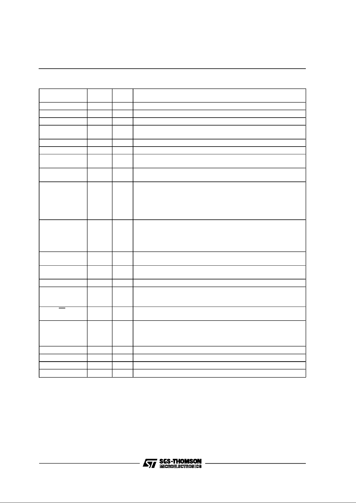
BLOCK DIAGRAM (ETC5064 - ETC5064-X - ETC5067 - ETC5067-X)
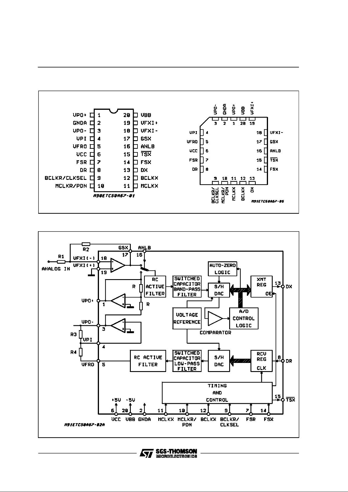
PIN CONNECTIONS (Top views)
DIP 20 &
SO20
PLCC20
ETC5064 - ETC5064-X - ETC5067 - ETC5067-X
2/18
Page 3
PIN DESCRIPTION
Name
Pin
Type (*)
N Description
VPO
+
O 1 The Non-inverting Output of the Receive Power Amplifier
GNDA GND 2 Analog Ground. All signals are referenced to this pin.
VPO
-
O 3 The Inverting Output of the Receive Power Amplifier
VPI I 4 Inverting Input to the Receive Power Amplifier. Also powers down both
amplifiers when connected to V
BB
.
VF
R
O O 5 Analog Output of the Receive Filter.
V
CC
S 6 Positive Power Supply Pin. VCC=+5V±5%
FS
R
I 7 Receive Frame Sync Pulse which enableBCLKRto shift PCM data into
D
R
.FSRis an 8KHz pulse train. See figures 1 and 2 for timing details.
D
R
I 8 Receive Data Input. PCM data is shifted into DRfollowing the FSRleading
edge
BCLK
R
/CLKSEL I 9 The bit Clock which shifts data into DRafter the FSRleading edge. May
vary from 64KHz to 2.048MHz.
Alternatively, may be a logic input which selectseither 1.536MHz/1.544MHz
or 2.048MHz for master clock in synchronous mode and BCLK
X
is used
for both transmit and receive directions (see table 1). This input has an
internal pull-up.
MCKL
R
/PDN I 10 Receive Master Clock. Must be 1.536MHz, 1.544MHz or 2.048MHz. May
be asynchronous with MCLK
X
, but should be synchronous with MCLKXfor
best performance. When MCLK
R
is connected continuously low, MCLKXis
selected for all internal timing. When MCLK
R
is connected continuously
high, the device is powered down.
MCLK
X
I 11 Transmit Master Clock. Must be 1.536MHz, 1.544MHz or 2.048MHz. May
be asynchronous with MCLK
R
.
BCLK
X
I 12 The bit clock which shifts out the PCM data on DX. May vary from 64KHz
to 2.048MHz, but must be synchronous with MCLK
X
.
D
X
O 13 The TRI-STATEPCM data output which is enabled by FSX.
FS
X
I 14 Transmit frame sync pulse input whichenables BCLKXto shift out the
PCM data on D
X
.FSXis an 8KHz pulse train. See figures 1 and 2 for
timing details.
TS
X
O 15 Open drain output which pulses low during the encoder time slot. Must to
be grounded if not used.
ANLB I 16 Analog Loopback Control Input. Must be set to logic ’0’ for normal
operation. When pulled to logic ’1’, the transmit filter input is disconnected
from the output of the transmit preamplifier and connected to the VPO
+
output of the receive power amplifier.
GS
X
O 17 Analog output of the transmit input amplifier. Used to set gain externally.
VF
X
I
-
I 18 Inverting input of the transmit input amplifier.
VF
X
I
+
I 19 Non-inverting input of the transmit input amplifier.
V
BB
S 20 Negative Power Supply Pin. VBB= -5V ±5%
(*) I: Input, O: Output, S: Power Supply.
TRI-STATE is a trademark of National Semiconductor Corp.
ETC5064 - ETC5064-X - ETC5067 - ETC5067-X
3/18
Page 4

FUNCTIO NAL DE SCRIPTION
POWER-UP
Whenpowerisfirstapplied,power-onresetcircuitry
initializes the device and places it into the powerdown mode. All non-essential circuits are deactivatedand the D
X
andVFRO outputsare put in high
impedancestates.Topower-upthedevice,alogical
low level or clock must be applied to the
MCLK
R
/PDN pin andFSXand/orFSRpulsesmust
bepresent.Thus2 power-downcontrolmodesare
available.The first is to pull the MCLK
R
/PDN pin
high;the alternativeis toholdboth FS
X
andFSRinputs continuouslylow. The device will power-down
approximately 2 ms after the last FS
X
pulse. The
TRI-STATEPCMdataoutput, D
X
, willremainin the
highimpedancestate untilthe secondFS
X
pulse.
SYNCHRONOUSOPERATION
For synchronousoperation,the same masterclock
and bit clock shouldbe used for boththe transmit
andreceivedirections.In thismode,a clockmustbe
appliedto MCLK
X
andthe MCLKR/PDNpin can be
used as a power-down control. A low level on
MCLK
R
/PDNpowersup thedevice anda high level
powersdownthedevice.In eithercase,MCLKXwill
beselectedasthemasterclockforboththetransmit
andreceivecircuits.A bitclockmustalsobeapplied
toBCLK
X
andtheBCLR/CLKSELcanbe usedtose-
lect theproper internal dividerfor a master clock of
1.536 MHz, 1.544 MHz or 2.048 MHz. For 1.544
MHz operation, the device automaticallycompensatesfor the 193 rd clock pulse each frame.
Withafixedlevel onthe BCLK
R
/CKSELpin,BCLK
X
willbe selectedasthe bit clock for boththe transmit
and receivedirections. Table 1 indicates the frequenciesof operation which can be selected, dependingonthestateofBCLK
R
/CLKSEL.Inthissyn-
chronousmode, the bit clock,BCLK
X
, may be from
64kHzto2.048MHz,butmustbesynchronouswith
MCLK
X
.
EachFS
X
pulsebegins the encodingcycle and the
PCM dat a from theprevious encodecycle isshiftout
of the enabled D
X
output on the positive edge of
BCLK
X
. After8 bit clock periods, the TRISTATED
X
outputis returnedto a high impedancestate.With an
FS
R
pulse, PCMdata is latched via the DRinputon
thenegat i veedgeofBCLK
X
(or on BCKLRifrunning).
FS
X
andFSRmustbe sy nc hronouswit hMCLKX/R.
ASYNCHRONOUSOPERATION
Forasynchronousoperation,separatetransmitand
receiveclocksmaybe applied.MCLK
X
andMCLK
R
mustbe2.048MHzforthe ETC5067or1.536MHz,
1.544MHz for the ETC5064, andneed not be synchronous.Forbesttransmissionperformance,however,MCLK
R
shouldbe synchronouswithMCLKX,
which iseasilyachievedby applyingonlystaticlogic
levelstotheMCLK
R
/PDNpin.Thiswillautomatically
connectMCLK
X
toallinternalMCLKRfunctions(see
pin description). For 1.544MHz operation,the deviceautomaticallycompensatesforthe 193rdclock
pulse each frame. FS
X
startseach encodingcycle
andmust besynchronouswith MCLK
X
andBCLKX.
FS
R
starts each decodingcycle and must be syn-
chronouswithBCLK
R
.BCLKRmust bea clock, the
logiclevels shown in Table 1 are not validin asynchronous mode. BCLK
X
and BCLKRmay operate
from 64kHzto 2.048 MHz.
SHORTFRAME SYNCOPERATION
The device can utilize either a short frame sync
pulseoralongframesyncpulse.Uponpowerinitialization,the deviceassumes a shortframemode. In
this mode,both frame sync pulses. FS
X
and FSR,
mustbe one bit clock periodlong, with timing relationshipsspecifiedin figure 2. With FS
X
highduring
a falling edge of BCLK
R
, the next rising edge of
BCLK
X
enablesthe DXTRI-STATE output buffer,
whichwilloutputthesignbit.Thefollowingsevenrising edgesclock out the remaining seven bits, and
the next falling edge disables the D
X
output. With
FS
R
highduringa falling edge ofBCLKR(BCLKXin
synchronousmode), thenextfallingedgeofBCLK
R
latches in the sign bit. The following seven falling
edges latch in the seven remaining bits. Both devicesmay utilizethe shortframe sync pulsein synchronousor asynchronousoperatingmode.
LONGFRAMESYNC OPERATION
To use the long frame mode, both the frame sync
pulses,FS
X
andFSR,mustbethreeormorebitclock
periods long, with timing relationships specified in
figure3. Basedonthe transmitframesyncFS
X
,the
devicewill sensewhether short or longframe sync
Table1: Selectionof MasterClock Frequencies.
BCLKR/CLKSEL
Master Clock
Frequency Selected
ETC5067
ETC5067-X
ETC5064
ETC5064-X
Clocked 2.048MHz 1.536MHz or
1.544MHz
0 1.536MHz or
1.544MHz
2.048MHz
1 (or open circuit) 2.048MHz 1.536MHz or
1.544MHz
ETC5064 - ETC5064-X - ETC5067 - ETC5067-X
4/18
Page 5

pulses are being used. For 64 kHz operation, the
framesync pulsesmust be kept low fora minimum
of 160 ns (see Fig 1). The D
X
TRI-STATE output
bufferis enabledwiththe risingedge of FS
X
or the
rising edgeof BCLK
X
, whichever comes later, and
the first bitclocked out is the sign bit. The following
sevenBCLK
X
risingedgesclockout the remaining
sevenbits. The D
X
outputis disabled by thefalling
BCLK
X
edge following the eighth risingedge,or by
FS
X
goinglow,whichevercomeslater.Arisingedge
onthereceiveframesyncpulse,FS
R
, will cause the
PCM data at D
R
to be latched in on the next eight
falling edges of BCLK
R
(BCLKxin synchronous
mode).Bothdevicesmay utilizethelongframesync
pulsein synchronousor asynchronousmode.
TRANSMITSECTION
Thetransmitsectioninputisanoperationalamplifier
withprovisionforgainadjustmentusingtwoexternal
resistors,seefigure4.Thelownoiseandwidebandwidth allow gains in excess of 20 dB across the
audiopassband to be realized.The op amp drives
a unity gain filter consisting of RC active pre-filter,
followed by an eighth order switched-capacitor
bandpassfilterdirectlydrives the encodersampleand-holdcircuit. TheA/D is of compandingtypeaccordingto A-law(ETC5067and ETC5067-X)or µlaw (ETC5064 and ETC5064-X) coding conventions. A precision voltage reference is trimmed in
manufacturingto providean inputover load (t
MAX
)
of nominally2.5V peak (see table of Transmission
Characteristics).The FS
X
framesyncpulsecontrols
thesamplingofthefileroutput,andthenthesuccessive-approximationencodingcyclebegins.The8-bit
code is then loaded into a buffer and shifted out
throughD
X
atthenextFSXpulse.thetotal encoding
delaywillbe approximately165µs (dueto thetransmitfilter)plus125µs(due toencodingdelay),which
totals290µs.Any offsetvoltagedue to thefiltersor
comparator iscancelledby signbit integration.
RECEIVESECTION
The receive section consistof an expandingDAC
which drives a fifth order switched-capacitor low
passfilter clocked at256kHz. Thedecoderis A-law
(ETC5067 and ETC5067-X) or µ–law (ETC5064
and ETC5064-X)and the 5 th orderlow passfilter
corrects for the sin x/xattenuationdue tothe 8kHz
sampleand hold. The filter is then followedby a 2
nd order RC active post-filter and power amplifier
capableofdriving a600Ω loadtoa levelof 7.2dBm.
The receive section is unity-gain. Upon the occurenceof FS
R
, the data at theDRinputis clocked
in on the falling edge of the next eight BCLK
R
(BCKLX)periods.Attheendofthedecodertimeslot,
the decoding cycle begins,and 10µs later the decoderDACoutputis updated.Thetotaldecoder delay is about10µs (decoderup-date)plus 110µs (fil-
ter delay) plus 62.5µs (1/2 frame),which givesapproximately180µs.
RECEIVEPOWER AMPLIFIERS
Two invertingmode power amplifiersareprovided
for directly driving a matched line interface transformer.The gain of thefirst power amplifier can be
adjustedtoboostthe± 2.5Vpeakoutputsignalfrom
thereceivefilterup± 3.3Vpeakintoanunbalanced
300Ωload,or±4.0Vintoan unbalanced15kΩ load.
Thesecondpower amplifier isinternally connected
in unity-gain inverting mode to give 6dB of signal
gainforbalancedloads.Maximumpowertransferto
a 600Ω subscriber line termination is obtained by
differientiallydrivinga balancedtransformerwitha
√2 : 1 turns ratio,as shown in figure4.A totalpeak
powerof15.6dBmcan bedeliveredto theloadplus
termination.Both power amplifier can be powered
downindependentlyfromthePDNinputbyconnecting the VPI input to V
BB
saving approximately 12
mW of power.
ABSOLUTEMAXIMUM RATINGS
Symbol Parameter Value Unit
V
CC
VCCto GNDA 7 V
V
BB
VBBto GNDA -7 V
V
IN,VOUT
Voltage at any Analog Input or Output VCC+0.3to VBB-0.3 V
Voltage at any Digital Input or Output V
CC
+0.3to GNDA -0.3 V
T
oper
Operating Temperature Range: ETC5064/67
ETC5064-X/67-X
-25 to +125
-40 to +125
°C
°C
T
stg
Storage Temperature Range -65 to +150 °C
Lead Temperature (soldering, 10 seconds) 300 °C
ETC5064 - ETC5064-X - ETC5067 - ETC5067-X
5/18
Page 6
ELECTRICALOPERATING CHARACTERISTICS
V
CC
=5.0V±5%,VBB=-5V±5%,GNDA=0V,TA=0°Cto70°C (ETC5064-X/67-X:TA=–40°Cto85°),unless
otherwisenoted;typicalcharacteristicsspecifiedat V
CC
=5.0V, VBB=-5.0V,TA=25°C; allsignals arerefer-
encedto GNDA.
DIGITAL INTERFACE (All devices)
Symbol Parameter Min. Typ. Max. Unit
V
IL
Input Low Voltage 0.6 V
V
IH
Input High Voltage 2.2 V
V
OL
Output Low Voltage
I
L
= 3.2 mA D
X
IL= 3.2 mA, Open Drain TS
X
0.4
0.4
V
V
V
OH
Output High Voltage
IH = 3.2 mA D
X
2.4 V
I
IL
Input Low Current (GNDA ≤ VIN≤ VIL)all digital inputs
Except BCLK
R
–10 10 µA
I
IH
Input High Current (VIH≤ VIN≤ VCC) Except ANLB – 10 10 µA
I
OZ
Output Currentin High Impedance State (TRI-STATE)
(GNDA ≤ V
O
≤ VCC)D
X
–10 10 µA
ANALOG INTERFACE WITH TRANSMITINPUT AMPLIFIER (all devices)
Symbol Parameter Min. Typ. Max. Unit
I
I
XA Input Leakage Current VFxI+or VFxI
–
(– 2.5 V ≤ V ≤ + 2.5 V)
– 200 200 nA
R
I
XA Input Resistance VFXI+or VFXI
–
(– 2.5 V ≤ V ≤ + 2.5 V)
10 MΩ
R
O
XA Output Resistance (closed loop, unity gain) 1 3 Ω
R
L
XA Load Resistance GS
X
10 kΩ
C
L
XA Load Capacitance GS
X
50 pF
V
O
XA Output Dynamic Range (RL≥ 10 kΩ)GS
X
– 2.8 +2.8 V
A
V
XA Voltage Gain (VFXI+to GSX) 5000 V/V
F
U
XA Unity Gain Bandwidth 1 2 MHz
V
OS
XA Offset Voltage – 20 20 mV
V
CM
XA Common-mode Voltage – 2.5 2.5 V
CMRRXA Common-mode Rejection Ratio 60 dB
PSRRXA Power Supply Rejection Ratio 60 dB
ANALOG INTERFACE WITH RECEIVE FILTER (all devices)
Symbol Parameter Min. Typ. Max. Unit
R
O
RF Output Resistance VFRO13Ω
R
L
RF Load Resistance (VFRO=±2.5 V) 10 kΩ
C
L
RF Load Capacitance 25 pF
VOS
R
O Output DC Offset Voltage – 200 200 mV
ETC5064 - ETC5064-X - ETC5067 - ETC5067-X
6/18
Page 7

ANALOG INTERFACE WITH POWERAMPLIFIERS (all devices)
Symbol Parameter Min. Typ. Max. Unit
IPI Input Leakage Current (– 1.0 V ≤ VPI ≤ 1.0 V) – 100 100 nA
RIPI Input Resistance (– 1.0 ≤ VPI ≤ 1.0 V) 10 MΩ
VIOS Input Offset Voltage – 25 25 mV
ROP Output Resistance (inverting unity–gain at VPO
+
or VPO–)1Ω
F
C
Unity–gain Bandwidth, Open Loop (VPO–) 400 kHz
C
L
P Load Capacitance (VPO+or VPO–to GNDA)
R
L
≥ 1500 Ω
R
L
= 600 Ω
R
L
= 300 Ω
100
500
1000
pF
GAp
+
Gain VPO–to VPO+to GNDA, Level at VPO–= 1. 77 Vrms
(+ 3 dBmO)
– 1 V/V
PSRRp Power Supply Rejection of V
CC
or V
BB
(VPO–connected to VPI)
0 kHz – 4 kHz
0 kHz – 50 kHz
60
36
dB
POWER DISSIPATION (all devices)
Symbol Parameter Min. Typ. Max. Unit
I
CC
0 Power-down Current at ETC6064/67
ETC5064-X/67-X
0.5
0.5
1.5 mA
mA
I
BB
0 Power-down Current at ETC6064/67
ETC5064-X/67-X
0.05
0.05
0.3
0.4
mA
mA
I
CC
1 Active Current at ETC6064/67
ETC5064-X/67-X
7.0
7.0
10.0
12.0mAmA
I
BB
1 Active Current at ETC6064/67
ETC5064-X/67-X
7.0
7.0
10.0
12.0mAmA
ELECTRICAL OPERATING CHARACTERISTICS (Continued)
ETC5064 - ETC5064-X - ETC5067 - ETC5067-X
7/18
Page 8

All TIMING SPECIFICATIONS
Symbol Parameter Min. Typ. Max. Unit
1/t
PM
Frequency of master clocks
MCLK
X
and MCLK
R
Depends on the device used and the
BCLK
R
/CLKSEL Pin
1.536
2.048
1.544
MHz
t
WMH
Width of MasterClock High MCLKXand MCLK
R
160 ns
t
WML
Width of MasterClock Low MCLKXand MCLK
R
160 ns
t
RM
Rise Time of Master Clock MCLKXand MCLK
R
50 ns
t
FM
Fall Time of Master Clock MCLKXand MCLK
R
50 ns
t
PB
Period of Bit Clock 485 488 15.725 ns
t
WBH
Width of BitClock High (VIH= 2.2 V) 160 ns
t
WBL
Width of BitClock Low (VIL= 0.6 V) 160 ns
t
RB
Rise Time of Bit Clock (tPB= 488 ns) 50 ns
t
FB
Fall Time of Bit Clock (tPB= 488 ns) 50 ns
t
SBFM
Set-up time from BCLKXhigh to MCLKXfalling edge.
(first bit clock after the leading edge of FS
X
)
100 ns
t
HBF
Holding Time from Bit Clock Low to the Frame Sync
(long frame only)
0ns
t
SFB
Set-up Time from Frame Sync to Bit Clock (longframe only) 80 ns
t
HBFI
Hold Time from 3rd Period of Bit Clock FSXor FS
R
Low to Frame Sync (long frameonly)
100 ns
t
DZF
Delay Time to valid data from FSXor BCLKX, whichever
comes later and delay time from FSX to data output disabled
(C
L
= 0 pF to 150 pF)
20 165 ns
t
DBD
Delay Time from BCLKXhigh to data valid
(load = 150 pF plus 2 LSTTL loads)
0 150 ns
t
DZC
Delay Time from BCLKXlow to dataoutput disabled 50 165 ns
t
SDB
Set-up Time from DRvalid to BCLK
R/X
low 50 ns
t
HBD
Hold Time from BCLK
R/X
low to DRinvalid 50 ns
t
HOLD
Holding Time from Bit Clock High to Frame Sync (short frame only) 0 ns
t
SF
Set-up Time from FS
X/R
to BCLK
X/R
Low
(short frame sync pulse) - Note 1
80 ns
t
HF
Hold Time from BCLK
X/R
Low to FS
X/R
Low
(short frame sync pulse) - Note 1
100 ns
t
XDP
Delay Time to TSXlow (load = 150 pF plus 2 LSTTI loads) 140 ns
t
WFL
Minimum Width of the Frame Sync Pulse (low level)
(64 bit/s operating mode)
160 ns
Note : 1.For short frame sync timing. FSXand FSRmust go high while their respective bit clocks are high.
Figure 1 : 64 k bits/s TIMING DIAGRAM. (see next page for complete timing)
ETC5064 - ETC5064-X - ETC5067 - ETC5067-X
8/18
Page 9

Figure2 : ShortFrame SyncTiming.
ETC5064 - ETC5064-X - ETC5067 - ETC5067-X
9/18
Page 10

Figure 3 : Long FrameSync Timing.
ETC5064 - ETC5064-X - ETC5067 - ETC5067-X
10/18
Page 11

TRANSMISSION CHARACTERISTICS
(all devices)T
A
=0°Cto70°C (ETC5064-X/67-X:TA= –40°Cto85°), VCC=5V±5%,VBB=–5V±5%,
GNDA=0V,f=1.02kHz,V
IN
=0dBm0transmitinputamplifierconnectedforunity–gainnon–inverting.(unless
otherwisespecified).
AMPLITUDERESPONSE
Symbol Paramet er Mi n . T yp. Max. Un i t
Absolute Levels - Nominal 0 dBm0 is 4 dBm (600Ω).
0 dBm0
1.2276 Vrms
t
MAX
Max Overload Level
3.14 dBm0 ETC5067
3.17 dBm0 ETC5064
2.492
2.501
VPK
G
XA
Transmit Gain, Absolute (TA=25°C, VCC= 5V, VBB= -5V)
Input at GS
X
= 0dBm0 at 1020Hz
-0.15 0.15 dB
GXR Transmit Gain, Relative to GXA
f = 16Hz
f = 50Hz
f = 60Hz
f = 180Hz
f = 200Hz
f = 300Hz -3000Hz
f = 3200Hz (ETC5064-X/67-X)
f = 3300Hz
f = 3400Hz
f = 4000Hz
f = 4600Hz and up, measure response from oHz to 4000Hz
-
-
-
-2.8
-1.8
-0.15
-0.35
-0.35
-0.7
-40
-30
-26
-0.2
-0.1
0.15
0.20
0.05
0
-14
-32
dB
G
XAT
Absolute Transmit Gain Variation with Temperature
T
A
=0°C to +70°C
T
A
= –40°C to +85°C (ETC5064-X/67-X)
-0.1
-0.15
0.1
0.15
dB
G
XAV
Absolute Transmit Gain Variation with Supply Voltage
(V
CC
=5V±5%, VBB= -5V ±5%)
-0.05 0.05 dB
G
XRL
Transmit Gain Variation with Level
Sinusolidal Test Method Reference Level = -10dBm0
VF
X
I+= -40dBm0 to +3dBm0
VF
X
I+= -50dBm0 to -40dBm0
VF
X
I+= -55dBm0 to -50dBm0
-0.2
-0.4
-1.2
0.2
0.4
1.2
dB
G
RA
Receive Gain, Absolute (TA=25°C, VCC= 5V, VBB= -5V)
Input = Digital Code Sequence for 0dBm0 Signal at 1020Hz
-0.15 0.15 dB
G
RR
Receive Gain, Relative to G
RA
f = 0Hz to 3000Hz
f = 3200Hz (ETC5064-X/67-X)
f = 3300Hz
f = 3400Hz
f = 4000Hz
-0.15
-0.35
-0.35
-0.7
0.15
0.20
0.05
0
-14
dB
G
RAT
Absolute Receive Gain Variation with Temeperature
T
A
=0°C to +70°C
T
A
= –40°C to +85°C (ETC5064-X/67-X)
-0.1
-0.15
0.1
0.15
dB
G
RAV
Absolute Receive Gain Variation with Supply Voltage
(V
CC
=5V±5%, VBB= -5V ±5%)
-0.05 0.05 dB
G
RRL
Receive Gain Variation with Level
Sinusoidal Test Method; Reference Input PCM code
corresponds to an ideally encoded -10dBm0 signal
PCM level = -40dBm0 to +3dBm0
PCM level = -50dBm0 to -40dBm0
PCM level = -55dBm0 to -50dBm0
-0.2
-0.4
-1.2
0.2
0.4
1.2
dB
V
RO
Receive Filter Output at VFRORL= 10KΩ -2.5 2.5 V
ETC5064 - ETC5064-X - ETC5067 - ETC5067-X
11/18
Page 12

TRANSMI SS I ON CHARACTERI S TI CS (continued).
ENVELOPEDELAY DISTORTION WITH FREQUENCY
Symbol Parameter Min. Typ. Max. Unit
D
XA
Transmit Delay, Absolute (f = 1600 Hz) 290 315 µs
D
XR
Transmit Delay, Relative to D
XA
f = 500 Hz-600 Hz
f = 600 Hz-800 Hz
f = 800 Hz-1000 Hz
f = 1000 Hz-1600 Hz
f = 1600 Hz-2600Hz
f = 2600 Hz-2800 Hz
f = 2800 Hz-3000 Hz
195
120
50
20
55
80
130
220
145
75
40
75
105
155
µs
D
RA
Receive Delay, Absolute (f = 1600 Hz) 180 200 µs
D
RR
Receive Delay, Relative to D
RA
f = 500 Hz-1000 Hz
f = 1000 Hz-1600 Hz
f = 1600 Hz-2600 Hz
f = 2600 Hz-2800 Hz
f = 2800 Hz-3000 Hz
–40
–30
–25
–20
70
100
145
90
125
175
µs
NOISE
Symbol Parameter Min. Typ. Max. Unit
N
XP
Transmit Noise, P Message (A-LAW, VFXI+= 0 V) Weighted 1)
ETC5064
ETC5064-X
–74
–74
–69
–67
dBm0p
dBm0p
N
RP
Receive Noise, P Message Weighted
(A-LAW, PCM Code Equals Positive Zero)
– 82 – 79 dBm0p
N
XC
Transmit Noise, C Message Weighted
(µ-LAW,VFxI
+
=0V) ETC5064
ETC5064-X
12
12
1516dBrnC0
dBrnC0
N
RC
Receive Noise, C Message Weighted
(µ-LAW,PCM Code Equals Alternating Positive and Negative Zero) 8 11 dBrnC0
N
RS
Noise, Single Frequency
f = 0 kHz to 100 kHz, Loop around Measurement, VF
X
I+=0V
– 53 dBm0
PPSR
X
Positive Power Supply Rejection, Transmit (note 2)
V
CC
= 5.0 VDC+ 100 mVrms, f = 0 kHz-50 kHz
40 dBp
NPSR
X
Negative Power Supply Rejection, Transmit (note 2)
V
BB
= 5.0 VDC+ 100 mVrms, f = 0 kHz-50 kHz
40 dBp
PPSR
R
Positive Power Supply Rejection, Receive (PCM code equals
positive zero, V
CC
= 5.0 VDC+ 100 mVrms)
f = 0 Hz-4000Hz A LAW
µ LAW
f = 4 kHz-25 kHz
f = 25 kHz-50 kHz
40
40
40
36
dBp
dBc
dB
dB
NPSR
R
Negative Power Supply Rejection, Receive (PCM code equals
positive zero, V
BB
= – 5.0 VDC+ 100 mVrms)
f = 0 Hz-4000Hz A LAW
µ LAW
f = 4 kHz-25 kHz
f = 25 kHz-50 kHz
40
40
40
36
dBp
dBc
dB
dB
SOS Spurious out-of-band Signals at the Channel Output
0 dBm0, 300 Hz-3400 Hz input PCM applied at D
R
4600 Hz-7600 Hz
7600 Hz-8400 Hz
8400 Hz-100,000 Hz
–32
–40
–32
dB
dB
dB
ETC5064 - ETC5064-X - ETC5067 - ETC5067-X
12/18
Page 13

TRANSMIS S I O N CHARACTERIS TICS (continued).
DISTORTION
Symbol Parameter Min. Typ. Max. Unit
STD
X
or
STD
R
Signal to Total Distortion (sinusoidal test method)
Transmit or Receive Half-channel
Level = 3.0 dBm0
= 0 dBm0 to – 30 dBm0
= – 40 dBm0 XMT
RCV
= – 55 dBm0 XMT
RCV
33
36
29
30
14
15
dBp
(ALAW)
dBc
(µLAW)
SFD
X
Single Frequency Distortion, Transmit (TA=25°C) – 46 dB
SFD
R
Single Frequency Distortion, Receive (TA=25°C) – 46 dB
IMD Intermodulation Distortion
Loop Around Measurement, VF
X
I+= – 4 dBm0 to
– 21 dBm0, two Frequencies in the Range 300 Hz-3400 Hz
–41 dB
CROSSTALK
Symbol Parameter Min. Typ. Max. Unit
CT
X-R
Transmit to Receive Crosstalk, 0dBm0 Transmit
f = 300 Hz-3400 Hz, D
R
= Steady PCM Code ETC5064/67
ETC5064-X/67-X
–90 –75
–65dBdB
CT
R-X
Receive to Transmit Crosstalk, 0dBm0 Receive Level (note 2)
f = 300 Hz-3400 Hz, VF
X
I=0V ETC5064/67
ETC5064-X/67-X
–90 –70
–65dBdB
POWER AMPLIFIERS
Symbol Parameter Min. Typ. Max. Unit
V
OL
Maximum 0 dBm0 Level for Better than ± 0.1 dB Linearity Over
the Range 10 dBm0 to + 3 dBm0
(balanced load, R
L
connected between VPO+and VPO–)
R
L
= 600 Ω
R
L
= 1200 Ω
R
L
=30kΩ
33
3.5
4.0
Vrms
S/D
P
Signal/Distortion RL= 600 Ω, 0 dBm0 50 dB
Notes : 1. Measured by extrapolation from the distortion test results.
2. PPSRX, NPSRX, CTR–X measured with a –50dBm0 activating signal applied at VF
X
I
+
ENCODINGFORMAT AT DXOUTPUT
A-Law
(Including even bit inversion)
µLaw
V
IN
(at GSX) = + Full-scale 1 0 1 0 1 0 1 0 1 0 0 0 0 0 0 0
V
IN
(at GSX)=0V 1 1 0 1 0 1 0 1
01010101
11111111
01111111
V
IN
(at GSX) = – Full-scale 0 0 1 0 1 0 1 0 0 0 0 0 0 0 0 0
ETC5064 - ETC5064-X - ETC5067 - ETC5067-X
13/18
Page 14

APPLI CATI O N INFO RMATI ON
POWERSUPPLIES
Whilethe pinsat theETC506X familyare wellpro-
tectedagainstelectricalmisure,it is recommended
that the standardCMOS practice be followed, ensuringthatgroundisconnectedtothe devicebefore
any other connections are made. In applications
wheretheprintedcircuit boardmaybepluggedinto
a ”hot” socket with power and clocks already present, an extra long ground pin in the connector
shouldbe used.
All groundconnectionstoeach deviceshouldmeet
ata commonpointascloseas possibletotheGNDA
pin. This minimizes theinteractionof groundreturn
currentsflowingthrougha commonbusimpedance.
0.1µFsupplydecouplingcapacitorsshouldbe connectedfromthis commongroundpoint to VCC and
VBBas close to the device as possible.
For best performance, the ground point of each
CODEC/FILTERon a cardshouldbe connectedto
a commoncardgroundinstarformation,ratherthan
viaagroundbus.Thiscommongroundpointshould
be decoupledto VCC and VBB with 10µF capacitors.
For best performance,TSx should be grounded if
not used.
Figure 4 : TypicalAsynchronousApplication.
ETC5064 - ETC5064-X - ETC5067 - ETC5067-X
14/18
Page 15

SO20 PACKAGE MECHANICAL DATA
DIM.
mm inch
MIN. TYP. MAX. MIN. TYP. MAX.
A 2.65 0.104
a1 0.1 0.2 0.004 0.008
a2 2.45 0.096
b 0.35 0.49 0.014 0.019
b1 0.23 0.32 0.009 0.013
C 0.5 0.020
c1 45° (typ.)
D 12.6 13.0 0.496 0.510
E 10 10.65 0.394 0.419
e 1.27 0.050
e3 11.43 0.450
F 7.4 7.6 0.291 0.300
L 0.5 1.27 0.020 0.050
M 0.75 0.030
S8°(max.)
ETC5064 - ETC5064-X - ETC5067 - ETC5067-X
15/18
Page 16

PLCC20 PACKAGE MECHANICAL DATA
DIM.
mm inch
MIN. TYP. MAX. MIN. TYP. MAX.
A 9.78 10.03 0.385 0.395
B 8.89 9.04 0.350 0.356
D 4.2 4.57 0.165 0.180
d1 2.54 0.100
d2 0.56 0.022
E 7.37 8.38 0.290 0.330
e 1.27 0.050
e3 5.08 0.200
F 0.38 0.015
G 0.101 0.004
M 1.27 0.050
M1 1.14 0.045
ETC5064 - ETC5064-X - ETC5067 - ETC5067-X
16/18
Page 17

DIP20 PACKAGE MECHANICAL DATA
DIM.
mm inch
MIN. TYP. MAX. MIN. TYP. MAX.
a1 0.254 0.010
B 1.39 1.65 0.055 0.065
b 0.45 0.018
b1 0.25 0.010
D 25.4 1.000
E 8.5 0.335
e 2.54 0.100
e3 22.86 0.900
F 7.1 0.280
I 3.93 0.155
L 3.3 0.130
Z 1.34 0.053
ETC5064 - ETC5064-X - ETC5067 - ETC5067-X
17/18
Page 18

Information furnished is believed to be accurate and reliable. However, SGS-THOMSON Microelectronics assumes no responsibility for
the consequences of use of such information nor for any infringement of patents or other rights of third partieswhich may result from its
use. No license is granted by implication or otherwise under any patent or patent rights of SGS-THOMSON Microelectronics. Specifications mentioned in this publication are subject to change without notice. This publication supersedes and replaces all information previously supplied. SGS-THOMSON Microelectronics products are not authorized for use as critical components in life support devices or
systems without express written approval of SGS-THOMSON Microelectronics.
1994 SGS-THOMSON Microelectronics - All Rights Reserved
SGS-THOMSON Microelectronics GROUP OF COMPANIES
Australia - Brazil - France - Germany - Hong Kong - Italy- Japan - Korea - Malaysia - Malta - Morocco - The Netherlands - Singapore-
Spain - Sweden - Switzerland - Taiwan - Thaliand - United Kingdom - U.S.A.
ETC5064 - ETC5064-X - ETC5067 - ETC5067-X
18/18
 Loading...