

Datasheet ETC5057N, ETC5057FN, ETC5057D, ETC5054N, ETC5054FN Datasheet (SGS Thomson Microelectronics)
...Page 1
ETC5054
ETC5057
SERIAL INTERFACECODEC/FILTER
COMPLETE CODEC AND FILTERING SYSTEM (DEVICE)INCLUDING:
– Transmithigh-passand low-pass filtering.
– Receivelow-passfilterwith sin x/x correction.
– ActiveRC noise filters
– µ-laworA-lawcompatibl eCOderandDECoder .
– Internalprecisionvoltage reference.
– SerialI/O interface.
– Internalauto-zerocircuitry.
A-LAW 16 PINS (ETC5057FN,20 PINS)
µ-LAW WITHOUT SIGNALING, 16 PINS
(ETC5054FN,20 PINS)
MEETS OR EXCEEDS ALL D3/D4 AND
CCITT SPECIFICATIONS
±
5V OPERATION
LOW OPERATING POWER - TYPICALLY 60
mW
POWER-DOWN STANDBY MODE - TYPICALLY 3 mW
AUTOMATIC POWER-DOWN
TTL OR CMOS COMPATIBLE DIGITAL IN-
TERFACES
MAXIMIZES LINE INTERFACE CARD CIR-
CUIT DENSITY
0to70°C OPERATION
DESCRIPTION
The ETC5057/ETC5054 family consists of A-law
and µ–law monolithic PCM CODEC/filters utilizing
the A/D and D/A conversionarchitectureshown in
the block diagram below, and a serial PCM interface. The devices are fabricated using doublepoly CMOS process. The encode portion of each
device consists of an input gain adjust amplifier,
an active RC pre-filter which eliminates very high
frequency noise prior to entering a switched-capacitor band-pass filter that rejects signals below
200 Hz and above 3400 Hz. Also included are
auto-zerocircuitry and a compandingcoder which
samples the filtered signal and encodes it in the
companded A-law orµ–law PCM format. The decode portion of each device consists of an expanding decoder, which reconstructs the analog
signal from the companded A-law or µ–law code,
a low-pass filter which corrects for the sin x/x response of the decoder output and rejects signals
above 3400 Hz and is followed by a single-ended
power amplifier capable of driving low impedance
loads. The devices require 1.536 MHz, 1.544
MHz, or 2.048 MHz transmit and receive master
clocks, which may be asynchronous,transmit and
receive bit clocks which may vary from 64 kHz to
2.048 MHz, and transmit and receive frame sync
pulses. The timing of the frame sync pulses and
PCM data is compatible with both industry standard formats.
This is advanced information on a new product now in development or undergoing evaluation. Details are subject to change without notice.
March 2000
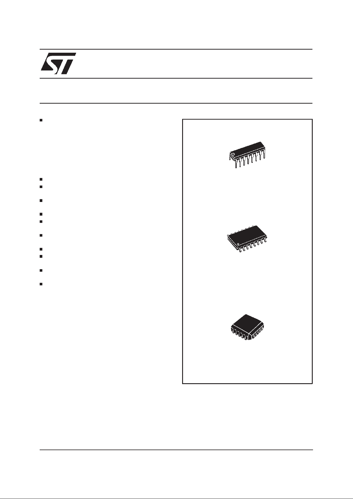
DIP16 (Plastic)
ORDERING NUMBERS:
ETC5057N
ETC5054N
SO16 (Wide)
ORDERING NUMBERS:
ETC5057D
ETC5054D
PLCC20
ORDERING NUMBERS:
ETC5057FN
ETC5054FN
1/18
Page 2
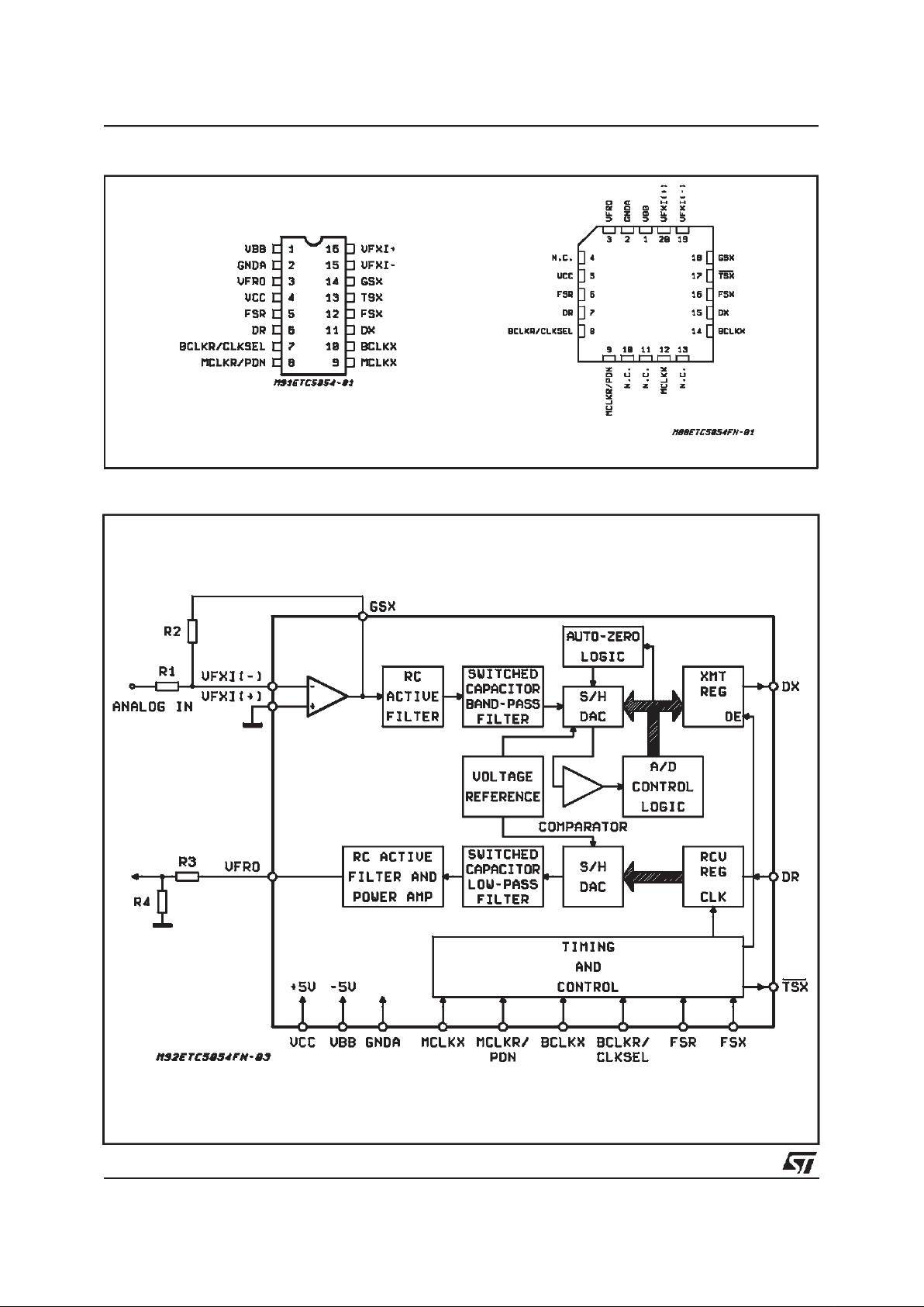
PIN CONNECTIONS (Topview)
DIP and SO
PLCC
BLOCKDIAGRAM
ETC5054 - ETC5057
2/18
Page 3
PIN DESCRIPTION
Name
Pin
Type
*
N
°
DIP
and
SO
N
°
PLCC
(**)
Function Description
V
BB
S 1 1 Negative
Power Supply
VBB=–5V±5%.
GNDA GND 2 2 Analog Ground All signals are referenced to this pin.
VF
R
O O 3 3 Receive Filter
Output
Analog Output of the Receive Filter
V
CC
S 4 5 Positive Power
Supply
VCC=+5V±5%.
FS
R
I 5 6 Receive Frame
Sync Pulse
Enables BCLKRto shift PCM data into DR.FSRis an
8kHz pulse train. See figures 1, 2 and 3 for timing
details.
D
R
I 6 7 Receive Data
Input
PCM data is shifted into DRfollowing the FSRleading
edge.
BCLK
R
/CLKSEL I 7 8 Shift-inClock Shifts data into DRafter the FSRleading edge. May
vary from 64 kHz to 2.048 MHz. Alternatively, may be
a logic input which selects either 1.536 MHz/1.544
MHz or 2.048 MHz for master clock in synchronous
mode and BCLK
X
is used for both transmit and receive
directions (see table 1). This input has an internal pullup.
MCLKR/PDN I 8 9 Receive Master Clock Must be 1.536 MHz, 1.544 MHz or 2.048 MHz. May be
asynchronous with MCLK
X
, but should be
synchronous with MCLK
X
for best performance. When
MCLK
R
is connected continuously low, MCLKXis
selected for all internal timing. When MCLK
R
is
connected continuously high, the device is powered
down.
MCLK
X
I 9 12 TransmitMaster Clock Must be 1.536 MHz, 1.544 MHz or 2.048 MHz. May be
asynchronous with MCLK
R
.
BCLK
XI
10 14 Shift-out Clock Shifts out the PCM data on DX. May vary from 64 kHz
to 2.048 MHz, but must be synchronous with MCLK
X
.
D
X
O 11 15 Transmit
Data Output
The TRI-STATE PCM data output which is enabled
by FS
X
.
FS
X
I 12 16 Transmit Frame
Sync Pulse
Enables BCLKXto shift out the PCM data on DX.FSXis
an 8 kHz pulse train. See figures 1, 2 and 3 for timing
details.
TS
X
O 13 17 Transmit Time Slot Open drain output which pulses low during the encoder
time slot. Recommended to be grounded if not used.
GS
X
O 14 18 Gain Set Analog output of the transmit input amplifier. Used to
set gain externally.
VF
X
I
–
I 15 19 Inverting Amplifier
Input
Inverting Input of the Transmit Input Amplifier.
VF
X
I
+
I 16 20 Non-inverting Amplifier
Input
Non-inverting Input of the Transmit Input Amplifier.
(*) I: Input, O: Output,S: Power Supply
(**) Pins 4,10,11 and 13 are not connected
TRI-STATEis a trademark of NationalSemiconductor Corp.
ETC5054 - ETC5057
3/18
Page 4

FUNCTIONAL DESCRIPTION
POWER-UP
When power is first applied, power-on reset cir-
cuitry initializes the device and places it into
the power-down mode. All non-essential circuits
are deactivatedand the D
X
and VFRO outputs are
put in high impedance states. To power-up the
device, a logical low level or clock must be applied to the MCLK
R
/PDN pin and FSXand/or FS
R
pulses must be present. Thus, 2 power-down
control modes are available. The first is to pull the
MCLK
R
/PDN pin high ; the alternative is to hold
both FS
X
and FSRinputs continuously low. The
device will power-down approximately 2 ms after
the last FS
X
or FSRpulse. Power-up will occur on
the first FS
X
or FSRpulse. The TRI-STATE PCM
data output, D
X
, will remain in the high impedance
state until the secondFS
X
pulse.
SYNCHRONOUS OPERATION
For synchronous operation, the same master
clock and bit clock should be used for both the
transmit and receive directions. In this mode, a
clock must be applied to MCLK
X
and the
MCLK
R
/PDN pin can be used as a power-down
control. A low level on MCLK
R
/PDN powers up
the device and a high level powers down the device. In either case, MCLK
X
will be selected as
the master clock for both the transmit and receive
circuits.A bit clock must also be applied to BCLK
X
and the BCLKR/CKSEL can be used to select the
proper internal divider for a master clock of 1.536
MHz, 1.544 MHz or 2.048 MHz. For 1.544 MHz
operation, the device automatically compensates
for the 193rd clock pulse each frame. With a fixed
level on the BCLK
R
/CLKSEL pin, BCLKXwill be
selected as the bit clock for both the transmit and
receive directions. Table 1 indicates the frequencies of operation which can be selected, depending on the state of BCLK
R
/CLKSEL. In this syn-
chronous mode, the bit clock, BCLK
X
, may be
from 64 kHz to 2.048 MHz, but must be synchronous with MCLK
X
.
Each FS
X
pulse begins the encoding cycle and
the PCM data from the previous encode cycle is
shifted out of the enabled D
X
output on the posi-
tive edge of BCLK
X
. After 8 bit clock periods, the
TRI-STATE D
X
output is returned to a high im-
pedance state. With and FS
R
pulse, PCM data is
latched via the D
R
input on the negative edge of
BCLK
X
(or BCLKRif running). FSXand FSRmust
be synchronouswith MCLK
X/R
.
ASYNCHRONOUSOPERATION
For asynchronous operation, separate transmit
and receive clocks may be applied, MCLK
X
and
MCLK
R
must be 2.048 MHz for the ETC5057, or
1.536 MHz, 1.544 MHz for the ETC5054, and
need not be synchronous. For best transmission
performance, however, MCLK
R
should be syn-
chronous with MCLK
X
, which is easily achieved
by applying only static logic levels to the
MCLK
R
/PDN pin. This will automatically connect
MCLK
X
to all internal MCLKRfunctions (see pin
description).For 1.544 MHz operation, the device
automatically compensates for the 193rd clock
pulse each frame. FS
X
startseach encoding cycle
and must be synchronous with MCLK
X
and
BCLK
X
.FSRstartseach decoding cycle and must
be synchronous with BCLK
R
. BCLKRmust be a
clock, the logic levels shown in table 1 are not
valid in asynchronous mode. BCLK
X
and BCLK
R
may operate from 64 kHz to 2.048 MHz.
SHORTFRAME SYNC OPERATION
The device can utilize either a short frame sync
pulse or a long frame sync pulse. Upon power initialization, the device assumes a short frame
mode. In this mode, both frame sync pulses, FS
X
and FSR, must be one bit clock period long, with
timing relationships specifiedin figure 2. With FS
X
high during a falling edge of BCLKXthe next rising edge of BCLK
X
enables the DXTRI-STATE
output buffer, which will output the sign bit. The
followingseven rising edges clock out the remaining seven bits, and the next falling edge disables
the D
X
output.With FSRhigh during a fallingedge
of BCLK
R
(BCLKXin synchronous mode), the
next falling edge of BCLK
R
latchesin the sign bit.
The following seven falling edges latch in the
seven remaining bits. Both devices may utilize the
short frame sync pulse in synchronous or asynchronousoperatingmode.
LONGFRAME SYNC OPERATION
To use the long frame mode, both the frame sync
pulses, FS
X
and FSR, must be three or more bit
clock periodslong, with timing relationships specified in figure 3. Basedon the transmit frame sync,
FS
X
, the device will sense whether short or long
frame sync pulses are being used. For 64 kHz operation,the frame sync pulse must be kept low for
a minimum of 160 ns (see fig. 1). The D
X
TRISTATE output buffer is enabled with the rising
edge of FS
X
or the rising edge of BCLKX, whichever comes later, and the first bit clocked out is
the sign bit. The following seven BCLK
X
rising
Table 1:SelectionofMasterClockFrequencies.
BCLKR/CLKSEL
Master Clock Frequency
Selected
ETC5057 ETC5054
Clocked
0
1 (or open circuit)
2.048 MHz
1.536 MHz or
1.544 MHz
2.048 MHz
1.536 MHz or
1.544 MHz
2.048 MHz
1.536 MHz or
1.544 MHz
ETC5054 - ETC5057
4/18
Page 5
edges clock out the remaining seven bits. The D
X
output is disabled by the falling BCLKXedge following the eighth rising edge, or by FS
X
going
low, which-evercomes later. A rising edge on the
receive frame sync pulse, FS
R
, will cause the
PCM data at D
R
to be latched in on the next eight
falling edges of BCLK
R
(BCLKXin synchronous
mode). Both devices may utilize the long frame
sync pulse in synchronous or asynchronous
mode.
TRANSMITSECTION
The transmit sectioninput is an operational ampli-
fier with provision for gain adjustment using two
external resistors, see figure6. The low noise and
wide bandwidth allow gains in excess of 20 dB
across the audio passband to be realized. The op
amp drives a unitygain filter consisting of RD active pre-filter, followed by an eighth order
switched-capacitorbandpassfilter clocked at 256
kHz. The outputof this filter directly drives the encoder sample-and-holdcircuit. The A/D is of companding type according to A-law (ETC5057)or µ–
law (ETC5054) coding conventions. A precision
voltage reference is trimmed in manufacturing to
provide an input overload (t
MAX
) of nominally2.5V
peak (see table of transmission characteristics).
The FS
X
frame sync pulse controls the sampling
of the filter output, and then the successive-ap-
proximation encoding cycle begins. The 8-bit
code is then loaded into a buffer and shifted out
through D
X
at the next FSXpulse. The total encoding delay will be approximately 165 µs (due to
the transmit filter) plus 125µs (due to encoding
delay), which totals 290µs. Any offset vol-tage
due to the filters or comparator is cancelled by
sign bit integration.
RECEIVESECTION
The receive section consists of an expanding
DAC which drives a fifth order switched-capacitor
low pass filter clocked at 256 kHz. The decoder is
A-law (ETC5057) or µ–law (ETC5054) and the
5th order low pass filter corrects for the sin x/x attenuation due to the 8 kHz sample and hold.
The filter is then followedby a2nd order RC active post-filterand power amplifier capable of driving a 600Ω load to a level of 7.2 dBm. The receive section is unity-gain.Upon the occurenceof
FS
R
, the data at the DRinput is clocked in on the
falling edge of the next eight BCLK
R
(BCLKX)periods. At the end of the decoder time slot, the decoding cycle begins, and 10µs later the decoder
DAC output is updated. The total decoder delay
is∼10µs (decoder update) plus 110µs (filter
delay) plus 62.5µs (1/2 frame), which gives ap-
proximately 180µs. A mute circuitry is a active
during 10ms when power up.
ABSOLUTE MAXIMUM RATINGS
Symbol Parameter Value Unit
V
CC
VCCto GNDA 7 V
V
BB
VBBto GNDA – 7 V
V
IN,VOUT
Voltage at any AnalogInput or Output VCC+ 0.3 to VBB– 0.3 V
Voltage at Any Digital Input or Output V
CC
+ 0.3 to GNDA – 0.3 V
T
oper
Operating Temperature Range – 25 to + 125
°
C
T
stg
Storage Temperature Range – 65 to + 150
°
C
Lead Temperature (soldering, 10 seconds) 300
°
C
ELECTRICALOPERATING CHARACTERISTICS VCC= 5.0 V ± 5%, VBB= – 5.0 V ± 5%GNDA= 0 V,
T
A
=0°Cto70°C; Typical Characteristics Specifiedat VCC=5.0 V, VBB= – 5.0 V, TA=25°C ; all signals
are referenced to GNDA.
Symbol Parameter Min. Typ. Max. Unit
V
IL
Input Low Voltage 0.6 V
V
IH
Input High Voltage 2.2 V
V
OL
Output Low Voltage
I
L
= 3.2mA D
X
IL= 3.2mA, Open Drain TS
X
0.4
0.4
V
V
V
OH
Output High Voltage
I
H
= 3.2mA D
X
2.4 V
I
IL
Input Low Current (GNDA ≤ VIN≤ VIL, all digital inputs) –10 10 µA
I
IH
Input High Current (VIH≤ VIN≤ VCC) except BCLKR/BCLKSEL –10 10 µA
I
OZ
Output Current in HIGH Impedance State (TRI-STATE)
(GNDA ≤ V
O
≤ VCC)D
X
–10 10 µA
ETC5054 - ETC5057
5/18
Page 6
ANALOG INTERFACEWITH TRANSMIT INPUT AMPLIFIER (all devices)
Symbol Parameter Min. Typ. Max. Unit
I
I
XA Input Leakage Current VFXI+or VFXI
-
(–2.5V ≤ V ≤ +2.5V)
– 200 200 nA
R
I
XA Input Resistance VFXI+or VFXI
-
(–2.5V≤V≤+2.5V)
10 MΩ
R
O
XA OutputResistance (closed loop, unity gain) 1 3
Ω
R
L
XA Load Resistance GS
X
10 k
Ω
C
L
XA Load Capacitance GS
X
50 pF
V
O
XA Output Dynamic Range (R
L
≥
10KΩ)GS
X
±
2.8 V
AV
X
A Voltage Gain (VFXI+to GSX) 5000 V/V
F
U
XA Unity Gain Bandwidth 1 2 MHz
V
OS
XA Offset Voltage – 20 20 mV
V
CM
XA Common-mode Voltage – 2.5 2.5 V
CMRRXA Common-mode Rejection Ratio 60 dB
PSRRXA Power Supply Rejection Ratio 60 dB
ANALOG INTERFACEWITH RECEIVE FILTER (all devices)
Symbol Parameter Min. Typ. Max. Unit
R
O
RF OutputResistance VFRO13Ω
R
L
RF Load Resistance (VFRO=±2.5V) 600 Ω
C
L
RF Load Capacitance 500 pF
VOS
R
O Output DC Offset Voltage – 200 200 mV
POWERDISSIPATION(all devices)
Symbol Parameter Min. Typ. Max. Unit
I
CC
0 Power-down Current 0.5 1.5 mA
I
BB
0 Power-down Current 0.05 0.3 mA
I
CC
1 ActiveCurrent 6.0 9.0 mA
I
BB
1 Active Current 6.0 9.0 mA
ETC5054 - ETC5057
6/18
Page 7

TIMING SPECIFICATIONS
Symbol Parameter Min. Typ. Max. Unit
1/t
PM
Frequency of master clocks
Depends on the device used and the BCLK
R
/CLKSEL Pin
MCLK
X
and MCLK
R
1.536
1.544
2.048
MHz
MHz
MHz
t
WMH
Width of Master Clock High MCLKXand MCLKR160 ns
t
WML
Width of Master Clock Low MCLKXand MCLKR160 ns
t
RM
Rise Time of Master Clock MCLKXand MCLK
R
50 ns
t
FM
Fall Time of Master Clock MCLKXand MCLK
R
50 ns
t
PB
Period of Bit Clock 485 488 15.725 ns
t
WBH
Width of Bit Clock High (VIH= 2.2V) 160 ns
t
WBL
Width of Bit Clock Low (VIL= 0.6V) 160 ns
t
RB
Rise Time of Bit Clock (tPB= 488ns) 50 ns
t
FB
Fall Time of Bit Clock (tPB= 488ns) 50 ns
t
SBFM
Set-up time from BCLKXhigh to MCLKXfalling edge.
(first bit clock after the leading edge of FS
X
)
100 ns
t
HBF
Holding Time from Bit Clock Low to the Frame Sync
(long frame only)
0ns
t
SFB
Set-up Time from Frame Sync to Bit Clock (long frame only) 80 ns
t
HBFI
Hold Time from 3rd Period of Bit Clock FSXor FS
R
Low to Frame Sync (long frame only)
100 ns
t
DZF
Delay time to valid data fromFSXorBCLKX, whichever comes later
and delay time from FS
X
to data outputdisabled.
(C
L
= 0pF to 150pF)
20 165 ns
t
DBD
Delay time from BCLKXhighto data valid.
(load = 150pF plus 2 LSTTL loads)
0 180 ns
t
DZC
Delay time from BCLKXlow to data output disabled. 50 165 ns
t
SDB
Set-up time from DRvalid to BCLK
R/X
low. 50 ns
t
HBD
Hold time from BCLK
R/X
low to DRinvalid. 50 ns
t
HOLD
Holding Time from Bit Clock High to FrameSync
(short frame only)
0ns
t
SF
Set-up Time from FS
X/R
to BCLK
X/R
Low
(short frame sync pulse) - Note 1
80 ns
t
HF
Hold Time from BCLK
X/R
Low to FS
X/R
Low
(short frame sync pulse) - Note 1
100 ns
t
XDP
Delay Time to TSXlow (load = 150pF plus 2 LSTTL loads) 140 ns
t
WFL
Minimum Width of the FrameSync Pulse (low level)
64kbit/s operating mode)
160 ns
Figure 1: 64kbits/sTIMINGDIAGRAM (see next pagefor complete timing).
Note 1: For short frame sync timing FSXand FSRmust go high while their respective bit clocks are high.
FSx
FS
R
ETC5054 - ETC5057
7/18
Page 8

Figure 2: ShortFrame Sync Timing
ETC5054 - ETC5057
8/18
Page 9

Figure 3: Long Frame Sync Timing
ETC5054 - ETC5057
9/18
Page 10

TRANSMISSIONCHARACTERISTICS
T
A
= 0 to 70°C, VCC= +5V ±5%, VBB= –5V ±5%, GNDA = 0V, f = 1.0KHz, VIN= 0dBm0 transmit input
amplifier connected for unity-gainnon-inverting(unless otherwise specified).
AMPLITUDERESPONSE
Symbol Parameter Min. Typ. Max. Unit
Absolute levels - nominal 0 dBm0 levelis 4 dBm (600 Ω)
0 dBm0
1.2276 Vrms
t
MAX
Max Overload Level
3.14 dBm0 (A LAW)
3.17 dBm0 (U LAW)
2.492
2.501
V
PK
V
PK
G
XA
Transmit Gain, Absolute (TA = 25 °C, VCC= 5 V, VBB=–5V)
Input at GS
X
= 0 dBm0 at 1020 Hz – 0.15 0.15 dB
G
XR
Transmit Gain, Relative to GXA
f = 16 Hz
f = 50 Hz
f = 60 Hz
f = 180 Hz
f = 200 Hz
f = 300 Hz - 3000 Hz
f = 3300 Hz
f = 3400 Hz
f = 4000 Hz
f = 4600 Hz and up, Measure Response from 0Hz to 4000 Hz
– 2.8
– 1.8
– 0.15
– 0.35
– 0.7
–40
–30
–26
– 0.2
– 0.1
0.15
0.05
0
–14
–32
dB
G
XAT
Absolute Transmit Gain Variation with Temperature
TA = 0 to +70°C – 0.1 0.1 dB
G
XAV
Absolute Transmit Gain Variationwith Supply Voltage
(V
CC
=5V±5%, VBB=–5V±5 %) – 0.05 0.05 dB
G
XRL
Transmit Gain Variations with Level
Sinusoidal Test Method Reference Level = – 10 dBm0
VFXI+ = – 40 dBm0 to + 3 dBm0
VF
X
I+ = – 50 dBm0 to – 40 dBm0
VF
X
I+ = – 55 dBm0 to – 50 dBm0
– 0.2
– 0.4
– 1.2
0.2
0.4
1.2
dB
dB
dB
G
RA
Receive Gain, Absolute (TA=25°C, VCC= 5V, VBB= –5V)
Input = Digital Code Sequence for 0dBm0 Signal at 1020Hz – 0.15 0.15 dB
G
RR
Receive Gain, Relative to GRA
f = 0Hz to 3000Hz
f = 3300Hz
f = 3400Hz
f = 4000Hz
– 0.35
– 0.35
– 0.7
0.20
0.05
0
–14
dB
dB
dB
dB
G
RAT
Absolute Transmit Gain Variationwith Temperature
T
A
= 0 to +70°C – 0.1 0.1 dB
G
RAV
Absolute Receive Gain Variation with Supply Voltage
(V
CC
=5V±5%, VBB=–5V±5 %) – 0.05 0.05 dB
G
RRL
Receive Gain Variations with Level
Sinusoidal Test Method; Reference input PCM code
corresponds to an ideally encoded – 10 dBm0 signal
PCM level = – 40 dBm0 to + 3dBm0
PCM level = – 50 dBm0 to – 40 dBm0
PCM level = – 55 dBm0 to – 50 dBm0
– 0.2
– 0.4
– 1.2
0.2
0.4
1.2
dB
dB
dB
V
RO
Receive Output Drive Level (RL= 600Ω) – 2.5 2.5 V
ETC5054 - ETC5057
10/18
Page 11

ENVELOPEDELAYDISTORTION WITH FREQUENCY
Symbol Parameter Min. Typ. Max. Unit
D
XA
Transmit Delay, Absolute (f = 1600Hz) 290 315
µ
s
D
XR
Transmit Delay, Relative to D
XA
f = 500Hz - 600Hz
f = 600Hz - 800Hz
f = 800Hz - 1000Hz
f = 1000Hz - 1600Hz
f = 1600Hz - 2600Hz
f = 2600Hz - 2800Hz
f = 2800Hz - 3000Hz
195
120
50
20
55
80
130
220
145
75
40
75
105
155
µs
D
RA
Receive Delay, Absolute (f = 1600Hz) 180 200
µ
s
D
RR
Receive Delay, Relative to D
RA
f = 500Hz - 1000Hz
f = 1000Hz - 1600Hz
f = 1600Hz - 2600Hz
f = 2600Hz - 2800Hz
f = 2800Hz - 3000Hz
–40
–30
–25
–20
70
100
145
90
125
175
µ
s
TRANSMISSION(continued)
NOISE
Symbol Parameter Min. Typ. Max. Unit
N
XP
Transmit Noise, P Message Weighted (A LAW, VFXI+= 0 V) 1) – 74 – 69 dBm0p
N
RP
Receive Noise, P Message Weighted
(A LAW, PCM code equals positive zero) – 82 – 79 dBm0p
N
XC
Transmit Noise, C Message Weighted µ LAW (VFXI+= 0 V) 12 15 dBmC0
N
RC
Receive Noise, C Message Weighted
(µ LAW, PCM Code Equals AlternatingPositive and Negative Zero) 8 11 dBrnC0
N
RS
Noise, Single Frequency
f = 0 kHz to 100 kHz, Loop around Measurement,
VF
X
I+= 0 Vrms – 53 dBm0
PPSR
X
Positive Power Supply Rejection, Transmit (note 2)
V
CC
= 5.0 VDC+ 100 mVrms, f = 0 kHz-50 kHz 40 dBp
NPSR
X
Negative Power Supply Rejection, Transmit (note2)
V
BB
= – 5.0VDC+ 100 mVrms,
f = 0 kHz-50 kHz 40 dBp
PPSR
R
Positive Power Supply Rejection,Receive
(PCM code equals positive zero, V
CC
= 5.0 VDC+ 100mVrms)
f = 0Hz to 4000Hz
f = 4KHz to25KHz
f = 25KHz to 50KHz
40
40
36
dBp
dB
dB
NPSR
R
Negative Power Supply Rejection, Receive
(PCM code equals positive zero, VBB = 5.0 VD
C
+ 100mVrms)
f = 0Hz to 4000Hz
f = 4KHz to25KHz
f = 25KHz to 50KHz
40
40
36
dBp
dB
dB
ETC5054 - ETC5057
11/18
Page 12

NOISE (continued)
Symbol Parameter Min. Typ. Max. Unit
SOS Spurius out-of-band Signalsat theChannel Output
Loop around measurement, 0dBm0, 300Hz - 3400Hz input applied
to DR, measure individual image signals at DX
4600Hz - 7600Hz
7600Hz - 8400Hz
8400Hz - 100,000Hz
–32
–40
–32
dB
dB
dB
TRANSMISSIONCHARACTERISTICS (continued)
DISTORTION
Symbol Parameter Min. Typ. Max. Unit
STD
X
or
STD
R
Signal to TotalDistortion (sinusoidal test method)
Transmit or Receive Half-channel
Level = 3.0dBm0
Level = 0dBm0 to –30dBm0
Level = –40dBm0 XMT
RCV
Level = –55dBm0 XMT
RCV
33
36
29
30
14
15
dBp
SFD
X
Single Frequency Distortion, Transmit (TA=25°C) –46 dB
SFD
R
Single Frequency Distortion, Receive (TA=25°C) –46 dB
IMD IntermodulationDistortion
Loop Around Measurement, VFXI+ = –4dBm0 to –21dBm0, two
Frequencies in the Range 300Hz - 3400Hz
–41 dB
CROSSTALK
Symbol Parameter Min. Typ. Max. Unit
CT
X-R
Transmit to Receive Crosstalk, 0 dBm0 Transmit Level
f = 300Hz to 3400Hz, D
R
= Steady PCM Mode – 90 – 75 dB
CT
R-X
Receive to Transmit Crosstalk, 0 dBm0 Receive Level
f = 300Hz to 3400Hz, (note2) – 90 – 70 dB
Notes:
1) Measured by extrapolation from distortiontest results.
2) PPSR
X
, NPSRX,CT
R-X
is measured with a –50dBm0 activating signal applied at VFXI+.
ENCODINGFORMATAT DXOUTPUT
A-Law (including even bit inversion)
µ
Law
V
IN
(at GSX) = +Full-scale 1 0 10101010000000
V
IN
(at GSX)=0V
1011001100110011101111111111111
1
V
IN
(at GSX) = – Full-scale 0 0 10101000000000
ETC5054 - ETC5057
12/18
Page 13

APPLICATIONINFORMATION
POWERSUPPLIES
While the pins at the ETC505X family are well
protected against electrical misuse, it is recommended that the standard CMOS practice be followed, ensuring that ground is connected to the
device before any-other connectionsare made. In
applications where the printed circuit board may
be plugged into a ”hot” socket with power and
clocks already present, an extra long ground pin
in the connector should be used.
All ground connections to each device should
meet at a common point as close as possible to
the GNDA pin. This minimizes the interaction of
ground return currents flowing through a common
bus impedance. 0.1µF supply decoupling capacitors should be connected from this common
ground point to V
CC
and VBBas close to the device as possible.
For best performance, the ground point of each
CODEC/FILTER on a card should be connected
to a commoncard ground in star formation,rather
than via a ground bus. This common ground point
should be decoupled to V
CC
and VBBwith 10µF
capacitors.
RECEIVEGAINADJUSTMENT
For applications where a ETC505X family
CODEC/filter receive output must drive a 600Ω
load, but a peak swing lower then±2.5V is required, the receive gain can be easily adjusted by
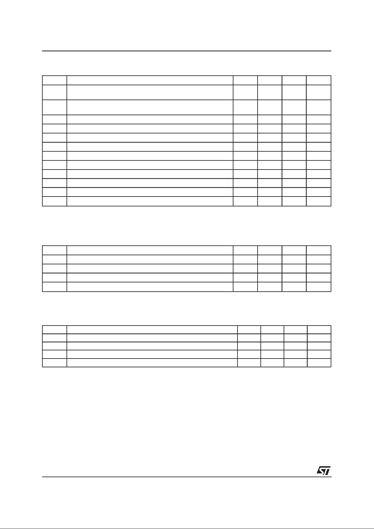
inserting a matched T-pad or π –pad at the output. Table II lists the required resistor values for
600Ω terminations. As these are generally nonstandard values, the equations can be used to
compute the attenuationof the closest pratical set
of resistors. It may be necessary to use unequal
valuesfor the R1 or R4 arms of the attenuatorsto
achieve a precise attenuation. Generally it is tolerable to allow a small deviation of the input impedance from nominal while still maintaining a
good return loss. For example a 30dB return loss
against 600Ω is obtained if the output impedance
of the attenuator is in the range 282Ωto 319
Ω
(assuminga perfect transformer).
Figure 4: T-PADAttenuator
Figure 5: Π-PADAttenuator
Table 2 : AttenuatorTables For
Z1 = Z2 = 300 Ω (all values in Ω).
dB R1 R2 R3 R4
0.1
0.2
0.3
0.4
0.5
0.6
0.7
0.8
0.9
1.0
2
3
4
5
6
7
8
9
10
11
12
13
14
15
16
18
20
1.7
3.5
5.2
6.9
8.5
10.4
12.1
13.8
15.5
17.3
34.4
51.3
68
84
100
115
129
143
156
168
180
190
200
210
218
233
246
26k
13k
8.7k
6.5k
5.2k
4.4k
3.7k
3.3k
2.9k
2.6k
1.3k
850
650
494
402
380
284
244
211
184
161
142
125
110
98
77
61
3.5
6.9
10.4
13.8
17.3
21.3
24.2
27.7
31.1
34.6
70
107
144
183
224
269
317
370
427
490
550
635
720
816
924
1.17k
1.5k
52k
26k
17.4k
13k
10.5k
8.7k
7.5k
6.5k
5.8k
5.2k
2.6k
1.8k
1.3k
1.1k
900
785
698
630
527
535
500
473
450
430
413
386
366
R1 = Z1
N
2
+ 1
N
2
−
1
−2 √Z1 . Z 2
N
N
2
−
1
R2=2
√
Z1.Z
2
N
N
2
− 1
Where: N =
√
POWERIN
POWEROUT
and: S =
√
Z1
Z2
Also : Z =
√
Z
SC
.
Z
OC
Where ZSC= impedancewith shortcircuit termination and Z
OC
= impedancewithopencircuitter-
mination.
R3
=
√
Z1 . Z 2
2
N
2
− 1
N
R3 = Z1
N
2
−
1
N
2
−
2NS+1
ETC5054 - ETC5057
13/18
Page 14

Figure 6: TypicalSynchronousApplication.
ETC5054 - ETC5057
14/18
Page 15

DIM.
mm inch
MIN. TYP. MAX. MIN. TYP. MAX.
A 2.35 2.65 0.093 0.104
A1 0.1 0.3 0.004 0.012
B 0.33 0.51 0.013 0.020
C 0.23 0.32 0.009
0.013
D 10.1 10.5 0.398 0.413
E 7.4 7.6 0.291 0.299
e 1.27 0.050
H 10 10.65 0.394 0.419
h 0.25 0.75 0.010 0.030
L 0.4 1.27 0.016 0.050
K0°(min.)8° (max.)
hx
45
A
e
B
D
E
A1
H
L
C
K
16
1
8
9
SO16 Wide
OUTLINE AND
MECHANICAL DATA
ETC5054 - ETC5057
15/18
Page 16

DIP16
DIM.
mm inch
MIN. TYP. MAX. MIN. TYP. MAX.
a1 0.51 0.020
B 0.77 1.65 0.030 0.065
b 0.5 0.020
b1 0.25 0.010
D 20 0.787
E 8.5 0.335
e 2.54 0.100
e3 17.78 0.700
F 7.1 0.280
I 5.1 0.201
L 3.3 0.130
Z 1.27 0.050
OUTLINE AND
MECHANICAL DATA
ETC5054 - ETC5057
16/18
Page 17

3212019
4
5
6
7
8
910111213
M1
M1
B
A
14
15
16
17
18
G (Seating Plane Coplanarity)
PLCC20ME
E
e
F
d2
d1
D
M
M
PLCC20
DIM.
mm inch
MIN. TYP. MAX. MIN. TYP. MAX.
A 9.78 10.03 0.385 0.395
B 8.89 9.04 0.350 0.356
D 4.2 4.57 0.165 0.180
d1 2.54 0.100
d2 0.56 0.022
E 7.37 8.38 0.290 0.330
e 1.27 0.050
F 0.38 0.015
G 0.101 0.004
M 1.27 0.050
M1 1.14 0.045
OUTLINE AND
MECHANICAL DATA
ETC5054 - ETC5057
17/18
Page 18

Information furnished is believed to be accurate and reliable. However, STMicroelectronics assumes no responsibility for the consequences
of use of such information nor for any infringement of patents or other rights of third parties which may result from its use. No license is
granted by implication or otherwise under any patent or patent rights of STMicroelectronics. Specification mentioned in this publication are
subject to change without notice. This publication supersedes and replaces all information previously supplied. STMicroelectronics products
are not authorized for use as critical components in life support devices or systems without express written approval of STMicroelectronics.
The ST logo is a registered trademark of STMicroelectronics
2000 STMicroelectronics – Printed in Italy – All Rights Reserved
STMicroelectronics GROUP OF COMPANIES
Australia - Brazil - China - Finland - France - Germany - Hong Kong - India - Italy - Japan - Malaysia - Malta - Morocco -
Singapore - Spain - Sweden - Switzerland - United Kingdom - U.S.A.
http://www.st.com
ETC5054 - ETC5057
18/18
 Loading...