

Page 1
NPN DARLINGTON POWER MODULE
■ HIGH CURRENTPOWER BIPOLAR MODULE
■ VERY LOW R
■ SPECIFIEDACCIDENTAL OVERLOAD
AREAS
■ ULTRAFASTFREEWHEELING DIODE
■ ISOLATEDCASE (2500V RMS)
■ EASY TO MOUNT
■ LOW INTERNAL PARASITIC INDUCTANCE
INDUSTRIALAPPLICATIONS:
■ MOTOR CONTROL
■ SMPS & UPS
■ WELDING EQUIPMENT
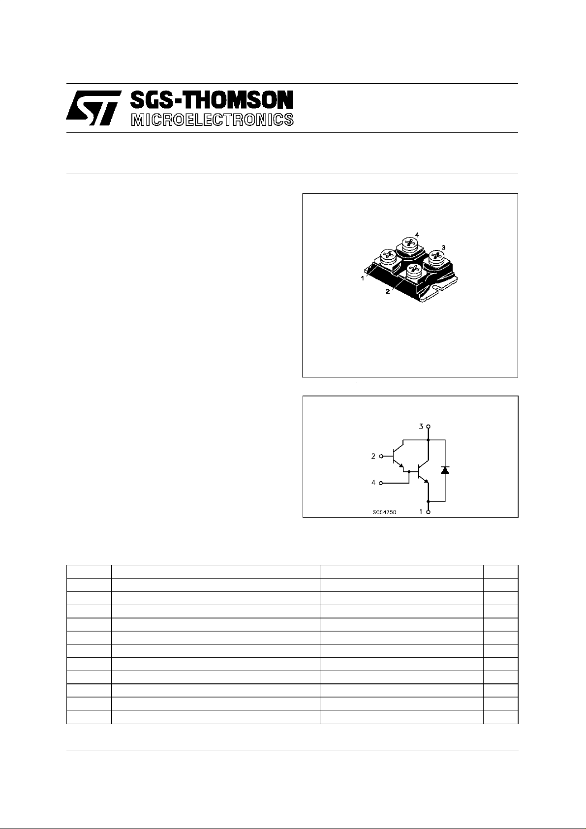
JUNCTION CASE
th
ESM5045DV
ISOTOP
INTERNAL SCHEMATIC DIAGRAM
ABSOLUTE MAXIMUM RATINGS
Symbol Parameter Value Unit
V
V
CEO(sus)
V
I
I
P
T
V
Collector-Emitter Voltage (VBE= -5 V) 600 V
CEV
Collector-Emitter Voltage (IB= 0) 450 V
Emitter-Base Voltage (IC=0) 7 V
EBO
Collector Current 60 A
I
C
Collector Peak Current(tp=10ms) 90 A
CM
Base Current 6 A
I
B
Base Peak Current (tp=10ms) 12 A
BM
Tota l Dissipat io n at Tc=25oC 175 W
tot
Storage Temperature -55 to 150
stg
Max. OperatingJunctionTemperature 150
T
j
Insulation WithstandVoltage (AC-RMS) 2500
ISO
o
C
o
C
o
C
September1997
1/8
Page 2

ESM5045DV
THERMAL DATA
R
thj-case
R
thj-case
R
thc-h
Thermal Resistance Ju nction-case (transistor) Max
Thermal Resistance Ju nction-case (diode) Max
Thermal Resistance Cas e-heatsinkWith Conductive
Grease Applied Max
0.71
1.2
0.05
o
C/W
o
C/W
o
C/W
ELECTRICAL CHARACTERISTICS (T
=25oC unless otherwise specified)
case
Symbol Parameter Test Conditions Min. Typ. Max. Unit
I
# Collector Cut-off
CER
I
CEV
I
EBO
V
CEO(SUS)
Curren t (R
BE
=5Ω)
# Collector Cut-off
Curren t (V
BE
=-5)
# Emitter Cut-off Current
(I
=0)
C
* Co lle cto r- Emitter
Sustaining Voltage
∗ DC Current Gain IC=50A VCE= 5 V 150
h
FE
V
∗ Collector-Emitter
CE(sat)
Saturation Voltage
V
∗ Ba se -Emit ter
BE(sat )
Saturation Voltage
di
/dt RateofRiseof
C
On-state Collector
(3 µs)••Collector-Emitter
V
CE
Dynamic Voltage
(5 µs)•• C o lle c t o r -Emitter
V
CE
Dynamic Voltage
Storage Time
s
Fall Time
t
f
Cross-over Time
c
Maximum Co llect or
V
t
t
CEW
Emitter Voltage
Without Snubber
∗ Diode Forward Voltage IF=50A Tj=100oC1.51.8V
V
F
I
RM
Reverse Recovery
Current
∗ Pulsed:Pulse duration= 300µs, duty cycle1.5%
Toevaluatethe conductionlosses ofthe diodeuse the followingequations:
V
= 1.5+ 0.0055IFP =1.5I
F
# Seetestcircuits in databookintroduction
F(AV)
+ 0.0055I
V
CE=VCEV
VCE=V
V
CE=VCEV
VCE=V
=5V 1 mA
V
EB
IC=0.2A L=25mH
V
= 450 V
clamp
IC=35A IB= 0.7 A
I
=35A IB=0.7A Tj= 100oC
C
I
=50A IB= 2.8 A
C
I
=50A IB=2.8A Tj= 100oC
C
IC=50A IB= 2.8 A
I
=50A IB=2.8A Tj= 100oC
C
VCC=300V RC=0 tp=3µs
I
=1.05A Tj= 100oC
B1
VCC= 300 V RC=8.5Ω
I
=1.05A Tj= 100oC
B1
VCC= 300 V RC=8.5 Ω
I
=1.05A Tj= 100oC
B1
I
= 35A VCC=50V
C
V
=-5V RBB=0.6Ω
BB
V
= 450 V IB1=0.7A
clamp
L = 0.07 mH T
I
=60A IB1=2.8A
CWo f f
V
=-5V VCC=50V
BB
L=42µHR
T
=125oC
j
VCC=200V IF=50A
di
/dt = -300 A/µsL<0.05µH
F
T
=100oC
j
2
F(RMS)
CEV
CEV
Tj= 100oC
Tj= 100oC
= 100oC
j
=0.6Ω
BB
450 V
1.2
1.4
1.4
1.6
2.3
2.3 3
300 400 A/µs
4.5 8 V
2.5 4.5 V
3.2
0.25
0.75
450 V
32 38 A
1.5
20
1
13
2
2
5
0.5
1.5
mA
mA
mA
mA
V
V
V
V
V
V
µs
µs
µs
2/8
Page 3
ESM5045DV
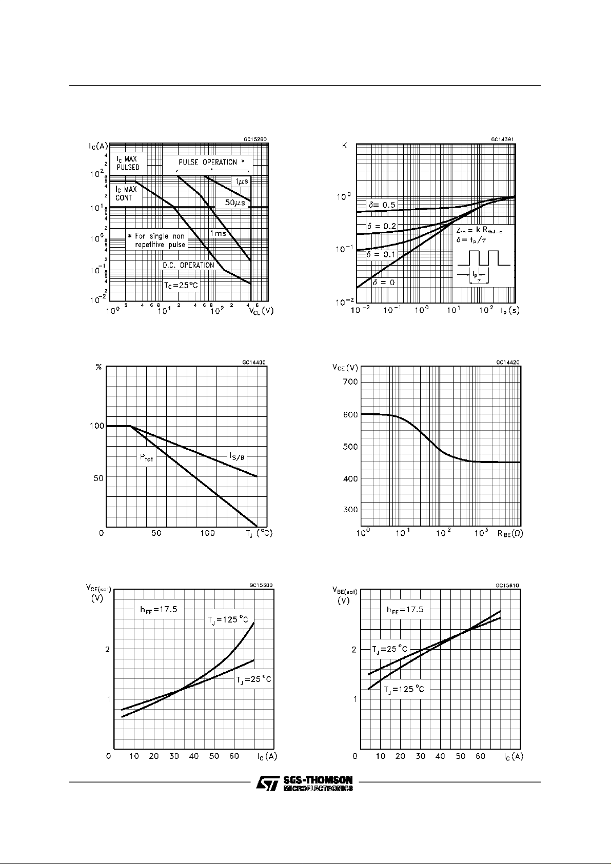
Safe OperatingAreas
Derating Curve
Thermal Impedance
Collector-emitter Voltage Versus
base-emitterResistance
CollectorEmitter Saturation Voltage
Base-Emitter SaturationVoltage
3/8
Page 4

ESM5045DV
ReverseBiased SOA
ReverseBiased AOA
FowardBiased SOA
ForwardBiased AOA
Switching Times Inductive Load
4/8
SwitchingTimes Inductive Load Versus
Temperature
Page 5

ESM5045DV
Dc Current Gain Typical VFVersus I
F
Peak Reverse Current Versus diF/dt Turn-onSwitching Test Circuit
Turn-on Switching Waveforms
5/8
Page 6

ESM5045DV
Turn-onSwitching Test Circuit Turn-offSwitching Waveforms
Turn-offSwitching Test Circuit of Diode Turn-offSwitching Waveform of Diode
6/8
Page 7

ISOTOPMECHANICALDATA
ESM5045DV
DIM.
MIN. TYP. MAX. MIN. TYP. MAX.
A 11.8 12.2 0.466 0.480
B 8.9 9.1 0.350 0.358
C 1.95 2.05 0.076 0.080
D 0.75 0.85 0.029 0.033
E 12.6 12.8 0.496 0.503
F 25.15 25.5 0.990 1.003
G 31.5 31.7 1.240 1.248
H 4 0.157
J 4.1 4.3 0.161 0.169
K 14.9 15.1 0.586 0.594
L 30.1 30.3 1.185 1.193
M 37.8 38.2 1.488 1.503
N 4 0.157
O 7.8 8.2 0.307 0.322
mm inch
G
A
B
O
N
D
E
F
H
J
C
K
L
M
7/8
Page 8

ESM5045DV
Informationfurnished is believed to be accurate andreliable. However, SGS-THOMSON Microelectronicsassumes no responsability for the
consequencesof use of such informationnor for any infringementof patents or otherrights of third partieswhich may results from its use.No
license isgrantedby implicationor otherwise underany patentor patentrights ofSGS-THOMSON Microelectronics.Specifications mentioned
in thispublication are subjectto change without notice. This publicationsupersedes and replacesall informationpreviously supplied.
SGS-THOMSON Microelectronicsproductsare notauthorizedforuse ascritical componentsin lifesupportdevices orsystems withoutexpress
written approvalof SGS-THOMSONMicroelectonics.
1997 SGS-THOMSONMicroelectronics - Printed in Italy- All Rights Reserved
Australia- Brazil - Canada - China- France- Germany- Hong Kong- Italy - Japan- Korea - Malaysia- Malta - Morocco - TheNetherlands -
Singapore - Spain- Sweden - Switzerland- Taiwan - Thailand- UnitedKingdom - U.S.A
SGS-THOMSONMicroelectronicsGROUP OF COMPANIES
...
8/8
 Loading...