

Page 1
NPN DARLINGTON POWER MODULE
■ HIGH CURRENT POWERBIPOLARMODULE
■ VERYLOW R
■ SPECIFIEDACCIDENTAL OVERLOAD
AREAS
■ ULTRAFASTFREEWHEELING DIODE
■ ISOLATEDCASE (2500VRMS)
■ EASY TOMOUNT
■ LOW INTERNAL PARASITICINDUCTANCE
APPLICATIONS:
■ MOTORCONTROL
■ SMPS& UPS
■ DC/DC &DC/AC CONVERTERS
■ WELDINGEQUIPMENT
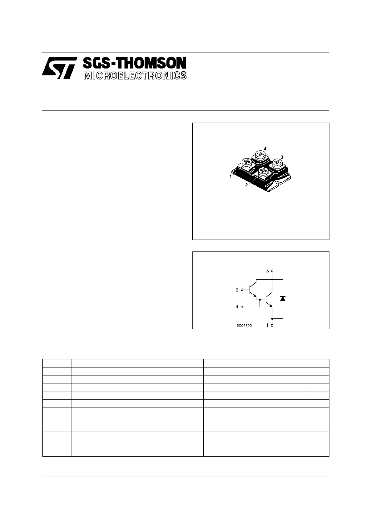
JUNCTIONCASE
th
ESM4045DV
ISOTOP
INTERNAL SCHEMATIC DIAGRAM
ABSOLUTE MAXIMUM RATINGS
Symb o l Parame t er Val u e Uni t
V
V
CEO(sus)
V
I
I
P
T
V
Collector-Emitter Voltage (VBE= -5 V) 600 V
CEV
Collector-Emitter Voltage (IB= 0) 450 V
Emitter-Base Voltage (IC=0) 7 V
EBO
Collect or Current 42 A
I
C
Collect or Peak Current ( tp=10ms) 63 A
CM
Base Current 4 A
I
B
Base Peak Current (tp=10ms) 8 A
BM
Total Dissipat ion at Tc=25oC 150 W
tot
Stora ge T emperat u re -55 to 150
stg
Max. Oper at i ng Junction T emperature 150
T
j
Insul at ion Withst and Voltage (AC-RMS) 2500
ISO
o
C
o
C
o
C
July 1997
1/8
Page 2

ESM4045DV
THERMAL DATA
R
thj-case
R
thj-case
R
thc-h
Thermal Resistance Junction-cas e (transistor) Max
Thermal Resistance Junction-case (diode) Max
Ther mal Res istance Cas e-hea tsink With Conductiv e
Gr ease Applied Max
0.83
1.5
0.05
o
C/W
o
C/W
o
C/W
ELECTRICAL CHARACTERISTICS (T
=25oC unlessotherwise specified)
case
Symbol Parameter Test Condition s Min. Typ. Max. Unit
I
# Collector Cut-off
CER
I
CEV
I
EBO
V
CEO(SUS)
Current (R
BE
=5Ω)
# Collector Cut-off
Current (V
BE
=-5)
# Emitter Cut-off Current
=0)
(I
C
* Collector-Emitter
Sust aining Volt ag e
∗ DC Current G ain IC=35A VCE= 5 V 220
h
FE
V
∗ Co llector- Emitt er
CE(sat)
Saturation Voltage
V
∗ Base-Emitt er
BE(sat )
Saturation Voltage
di
/dt Rate of Rise of
C
On-stat e Collector
(3 µs) Collector-Emitt er
V
CE
Dynamic Voltage
V
(5 µ s) Collect or- E mitt er
CE
Dynamic Voltage
St orage Time
s
t
Fall Time
f
Cross-over Time
c
Maximum Collector
V
t
t
CEW
Emit ter Voltage
Wit hout S nubber
V
∗ Diode For ward V oltage IF=35A Tj= 100oC1.51.85V
F
I
RM
Reverse Recovery
Current
∗
Pulsed: Pulse duration = 300 µs, duty cycle 1.5 %
To evaluate the conduction losses of the diode use the following equations:
= 1.5 + 0.001 IFP = 1.5 I
V
F
# See test circuits in databook introduction
F(AV)
+ 0.001 I
V
CE=VCEV
VCE=V
V
CE=VCEV
VCE=V
V
=5V 1 mA
EB
CEV
CEV
Tj=100oC
Tj=100oC
IC=0.2A L=25mH
= 450 V
V
clamp
IC=25A IB=0.5A
I
=25A IB=0.5A Tj=100oC
C
=35A IB=2A
I
C
I
=35A IB=2A Tj=100oC
C
IC=35A IB=2A
=35A IB=2A Tj= 100oC
I
C
VCC=300V RC=0 tp=3µs
=0.75A Tj=100oC
I
B1
VCC=300V RC=12Ω
=0.75A Tj=100oC
I
B1
VCC=300V RC=12Ω
=0.75A Tj=100oC
I
B1
IC=25A VCC=50V
=-5V RBB=0.6Ω
V
BB
V
= 450 V IB1= 0.5 A
clamp
L=0.1mH T
I
=42A IB1=2A
CWo f f
=-5V VCC=50V
V
BB
L = 0.06 mH R
= 125oC
T
j
=100oC
j
=0.6Ω
BB
VCC=200V IF=35A
di
/dt = -200 A/µ sL<0.05µH
F
= 100oC
T
j
2
F(RMS)
1.5
20
1
13
mA
mA
mA
mA
450 V
1.15
1.3
1.4
1.5
2.3
2.3 3
2
2
V
V
V
V
V
V
200 250 A/µ s
4.5 8 V
2.5 4.5 V
3.2
0.25
0.75
5
0.5
1.5
µs
µs
µs
450 V
20 24 A
2/8
Page 3
ESM4045DV
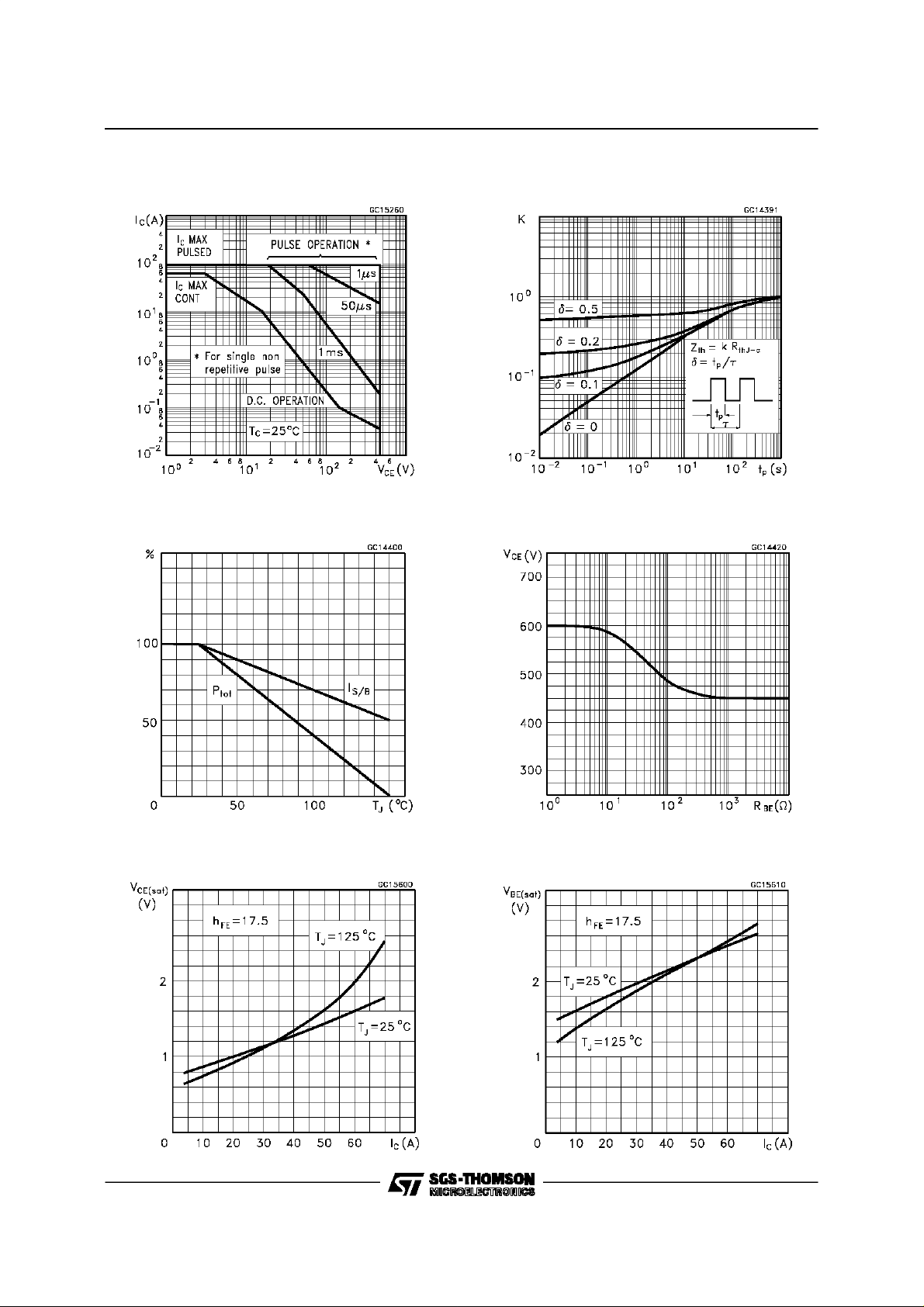
Safe OperatingAreas
Derating Curve
ThermalImpedance
Collector-emitter VoltageVersus
base-emitterResistance
CollectorEmitter SaturationVoltage
Base-EmitterSaturationVoltage
3/8
Page 4

ESM4045DV
ReverseBiased SOA
ReverseBiased AOA
FowardBiased SOA
ForwardBiased AOA
SwitchingTimes InductiveLoad
4/8
SwitchingTimes InductiveLoad Versus
Temperature
Page 5

ESM4045DV
Dc Current Gain TypicalV
VersusI
F
F
Peak Reverse Current Versus diF/dt Turn-onSwitching TestCircuit
Turn-onSwitching Waveforms
5/8
Page 6

ESM4045DV
Turn-onSwitching Test Circuit Turn-off Switching Waveforms
Turn-offSwitching TestCircuit ofDiode Turn-off Switching Waveformof Diode
6/8
Page 7

ISOTOPMECHANICAL DATA
ESM4045DV
DIM.
MIN. TYP. MAX. MIN. TYP. MAX.
A 11.8 12.2 0.466 0.480
B 8.9 9.1 0.350 0.358
C 1.95 2.05 0.076 0.080
D 0.75 0.85 0.029 0.033
E 12.6 12.8 0.496 0.503
F 25.15 25.5 0.990 1.003
G 31.5 31.7 1.240 1.248
H 4 0.157
J 4.1 4.3 0.161 0.169
K 14.9 15.1 0.586 0.594
L 30.1 30.3 1.185 1.193
M 37.8 38.2 1.488 1.503
N 4 0.157
O 7.8 8.2 0.307 0.322
mm inch
G
A
B
O
N
D
E
F
H
J
C
K
L
M
7/8
Page 8

ESM4045DV
Informationfurnished isbelieved to beaccurate and reliable.However, SGS-THOMSON Microelectronicsassumes no responsability for the
consequencesof useof such information nor for any infringementof patents or other rights of third parties which may results fromits use.No
license is grantedby implication or otherwiseunderanypatentor patentrights ofSGS-THOMSONMicroelectronics. Specificationsmentioned
in this publicationare subject to change withoutnotice. This publicationsupersedes and replacesall informationpreviously supplied.
SGS-THOMSON Microelectronicsproducts arenotauthorizedfor use ascritical componentsinlifesupportdevices or systemswithout express
written approvalof SGS-THOMSONMicroelectonics.
1997 SGS-THOMSONMicroelectronics -Printed in Italy- All Rights Reserved
Australia- Brazil - Canada- China- France - Germany- Hong Kong - Italy- Japan- Korea - Malaysia - Malta - Morocco - The Netherlands-
Singapore - Spain- Sweden - Switzerland- Taiwan - Thailand- UnitedKingdom- U.S.A
SGS-THOMSON Microelectronics GROUP OF COMPANIES
...
8/8
 Loading...