

Page 1
®
ESDA6V1U1
Applicati on Spec ific Di scretes
A.S.D.
APPLICATIONS
Where transient overvoltage protection in ESD
sensitive equipment is required, such as :
- COMPUTERS
- PRINTERS
- COMMUNICATION S YS TEM S
- GSM HA NDS ETS AND A CCE SS ORI ES
- CAR RA DIO
It is particulary recommended for parallel port
protection where the line interface withstands only
2 kV ESD surge.
FEATURES
6 UNIDIRECTIONAL TRANSIL FUNCTIONS
LOW LEAKAGE CURRENT: IR max. < 2 µA
200 W PEAK PULSE POWER (8/20 µs)
TRANSIL ARRAY
FOR ESD PROTECTION
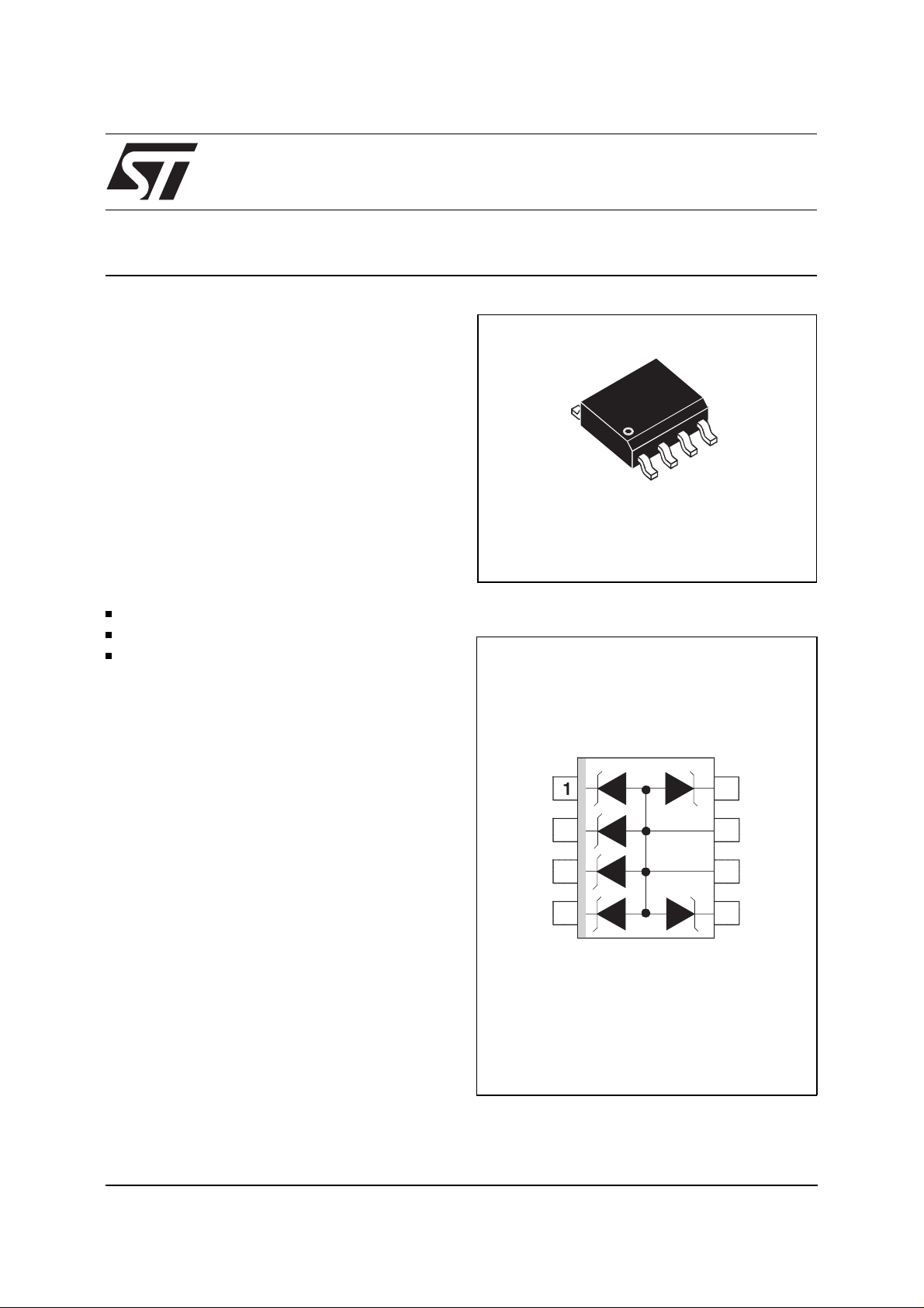
SO8
FUNCTIONAL DIAGRAM
DESCRITION
The ESDA6V1U1 is a monolithic voltage
suppressor designed to protect components whic h
are connected to data and transmission lines
against ESD.
It clamps the voltage just above the logic level
supply for positive transients, and to a diode drop
below ground for negative transients.
BENEFITS
High ESD protection level : up to 25 kV
High integration
Suitable for high density boards
COMPLIES WITH THE FOLLOWING STANDARDS :
IEC 1000-4-2 : level 4
MIL STD 883C-Method 3015-6 : class3
(human body model)
I/O 1
I/O 2
I/O 3
I/O 4
8
I/O 6
2
3
4
7
6
5
GND
GND
I/O 5
January 1998 - Ed : 2
1/6
Page 2
ESDA6V1U1
ABSOLUTE MAXIMUM RATINGS
(T
amb
= 25°C)
Symbol Parameter Value Unit
V
PP
Electrostatic discharge
25 kV
MIL STD 883C - Method 3015-6
P
PP
T
stg
T
j
T
L
ELECTRICAL CHARACTERISTICS
Peak pulse power (8/20µs) 200 W
Storage temperature range
Maximum junction temperature
- 55 to + 150
125
Maximum lead temperature for soldering during 10s 260 °C
(T
= 25°C)
amb
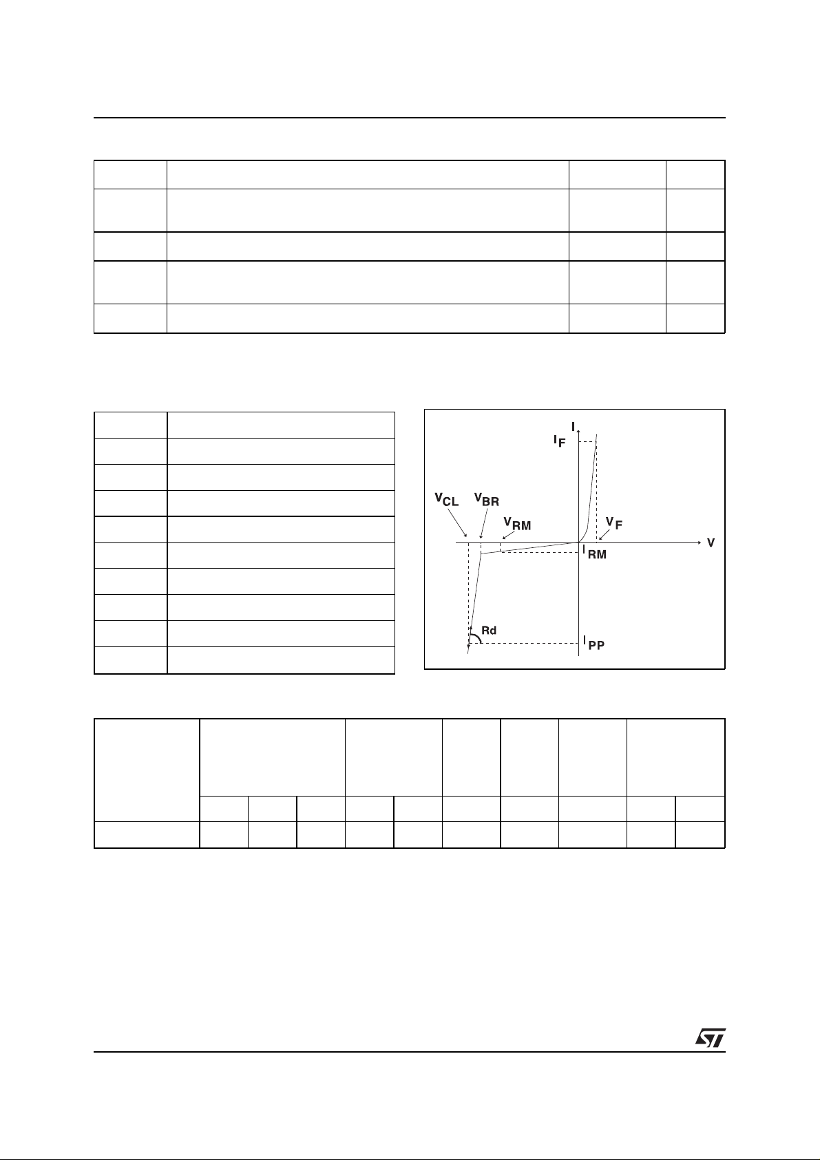
Symbol Parameter
V
RM
V
BR
V
CL
I
RM
Stand-off voltage
Breakdown voltage
Clamping voltage
Leakage current
°C
°C
I
PP
α
T Voltage temperature coefficient
Peak pulse current
C Capacitance
Rd Dynamic resistance
V
F
Types VBR @
Forward voltage drop
I
R
IRM @ V
RM
Rd αTCV
@ I
F
min. max. max. typ. max. typ. max.
note 1 note 2 0V bias
VVmAµAV Ω10
-4
/°CpF VmA
ESDA6V1U1 6.1 7.2 1 2 5 0.5 6 100 1.5 200
note 1
: Square pulse, Ipp = 25A, tp=2.5µs.
note 2
: ∆ V
= αT* (Tamb -25°C) * VBR (25°C)
BR
F
2/6
Page 3

ESDA6V1U1 ESDA6V1U1
CALCULATION OF THE CLAMPING VOLTAGE
USE OF THE DY NAM IC RE SIS TANCE
The ESDA family has been des igned t o c lamp fast
spikes like ESD. Generally the PCB designers
need to calculate easily the clamping voltage V
CL
This is why we give the dynamic resistance in
addition to the classical parameters. The voltage
across the protection cell can be calculated with
the following formula:
= VBR + Rd I
V
CL
PP
Where Ipp is the peak current through the ESDA cell.
DYNAMIC RESISTANCE MEAS UREMENT
The short duration of the ESD has led us to prefer
a more adapted test wave, as below defined, to the
classical 8/20µs and 10/1000µs surges.
I
Ipp
As the value of the dynamic resistance remains
stable for a surge duration lo wer than 20µs, the
.
2.5µs rectangular surge is well adapted. In addition
both rise and fall times are optimized to avoid any
parasitic phenomenon during the measurement of
Rd.
2µs
tp = 2.5µs
2.5µs duration measurement wave.
t
3/6
Page 4

ESDA6V1U1
Fig. 1 :
Peak power dissipation v ers us initial
junction temperature.
Ppp[Tj initial]/Ppp[Tj initial=25°C]
1.1
1.0
0.9
0.8
0.7
0.6
0.5
0.4
0.3
0.2
0.1
0.0
0 25 50 75 100 125 150
Fig. 3 :
Clamping voltage versus peak pulse
Tj initial(°C)
current (Tj initial = 25 °C).
Rectangular waveform tp = 2.5 µs.
Ipp(A)
50.0
10.0
tp=2.5µs
Fig. 2 :
Peak pulse power v ers us exponential
pulse duration (Tj initial = 25 °C).
Ppp(W)
2000
1000
100
10
110100
Fig. 4 :
Capacitance versus reverse applied
tp(µs)
voltage (typical values).
C(pF)
100
F=1MHz
Vosc=30mV
50
1.0
V (V)
0.1
4 6 8 1012141618202224262830
Fig. 5 :
Relative variation of leakage current
CL
versus junction temperature (typical values).
I [Tj] / I [Tj=25°C]
RR
200
100
10
Tj(°C)
1
25 50 75 100 125
20
V (V)
10
12 510
Fig. 6 :
Peak forward voltage drop versus peak
R
forward current (typical values).
I (A)
FM
5.00
Tj=25°C
1.00
0.10
V (V)
0.01
0.0 0.5 1.0 1.5 2.0 2.5 3.0
FM
4/6
Page 5

ESDA6V1U1 ESDA6V1U1
APPLICATION EXAMPL E :
D1
D2
Dn
Protection of logic-level signals.
ESDA6V1U1
0 to 5 V
0 to 5 V
0 to 5 V
APPLICATION EXAMPL E :
Note :
Capacitance value between any I/O pin and Ground is divided by 2.
Protection of symmetrical signals.
ESDA6V1U1
A1
A2
A3
A4
+/- 2.5 V
+/- 2. 5 V
+/- 2.5 V
+/- 2.5 V
5/6
Page 6

ESDA6V1U1
ORDER CODE
ESD ARR AY
MARKING :
PACKAGE MECHANICAL DAT A
SO8 Plastic
Logo, Date Code, E6VU1
ESDA
6 V
VBR min
1 U 1
REF.
Min. Typ. Max. Min. Typ. Max.
A 1.75 0.069
a1 0.1 0.25 0.004 0.010
a2 1.65 0.065
b 0.35 0.48 0.014 0.019
b1 0.19 0.25 0.007 0.010
C 0.50 0.020
c1 45° (typ )
D 4.8 5.0 0.189 0.197
E 5.8 6.2 0.228 0.244
e 1.27 0.050
e3 3.81 0.150
F 3.8 4.0 0.15 0.157
L 0.4 1.27 0.016 0.050
M 0.6 0.024
S8° (max)
RL
PACKAGING:
RL = Tape and reel
= Tube
PACKAGE: SO8 PLASTIC
Unidirectionel
DIMENSIONS
Millimetres Inches
Packaging :
Weight :
Information furnished is believed to be accurate and reliable. However, STMicroelectronics assumes no responsibility for the con sequen ces of
use of such information nor for any infringement of patents or other rights of third parties which may result from its use. No license is granted by
implication or otherwis e under any patent or patent rights of STMicroelectro nics. Specifications men tioned in this publication are subject to
change without notice. This publication supersedes and replaces all information previously supplied.
STMicroelectro nic s products are not authorized for us e as critical com ponent s i n l i fe s upport devices or sys tems without expres s written approval of STMicroelectronics.
Australia - Brazil - Canada - China - France - Germany - Italy - Japan - Korea - Malaysia - Malta - Mexico - Morocco - The
6/6
Preferred packaging is tape and reel.
0.08g.
© 1998 STMicroelectronics - Printed in Italy - All rights reserved.
STMicroelectronics GROUP OF COMPANIES
Netherlands - Singapore - Spain - Sweden - Switzerland - Taiwan - Thailand - United Kingdom - U.S.A.
 Loading...