

Page 1
®
ESDA6V1P6
Application Specific Discretes
A.S.D.
MAIN APPLICATIONS
Where transient overvoltage protection in ESD
sensitive equipment is required, such as :
Computers
■
Printers
■
Communication systems and cellular phones
■
Video equipment
■
Thisdeviceisparticularlyadpatedto the protection
of symmetrical signals.
FEATURES
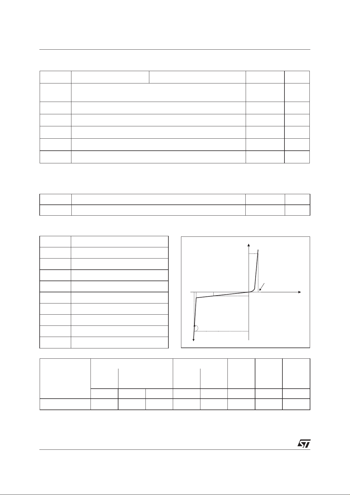
4UNIDIRECTIONAL TRANSIL™ FUNCTIONS.
■
■ BREAKDOWN VOLTAGE V
■ LOW LEAKAGE CURRENT < 500 nA
VERY SMALL PCB AREA < 2.6 mm
■
DESCRIPTION
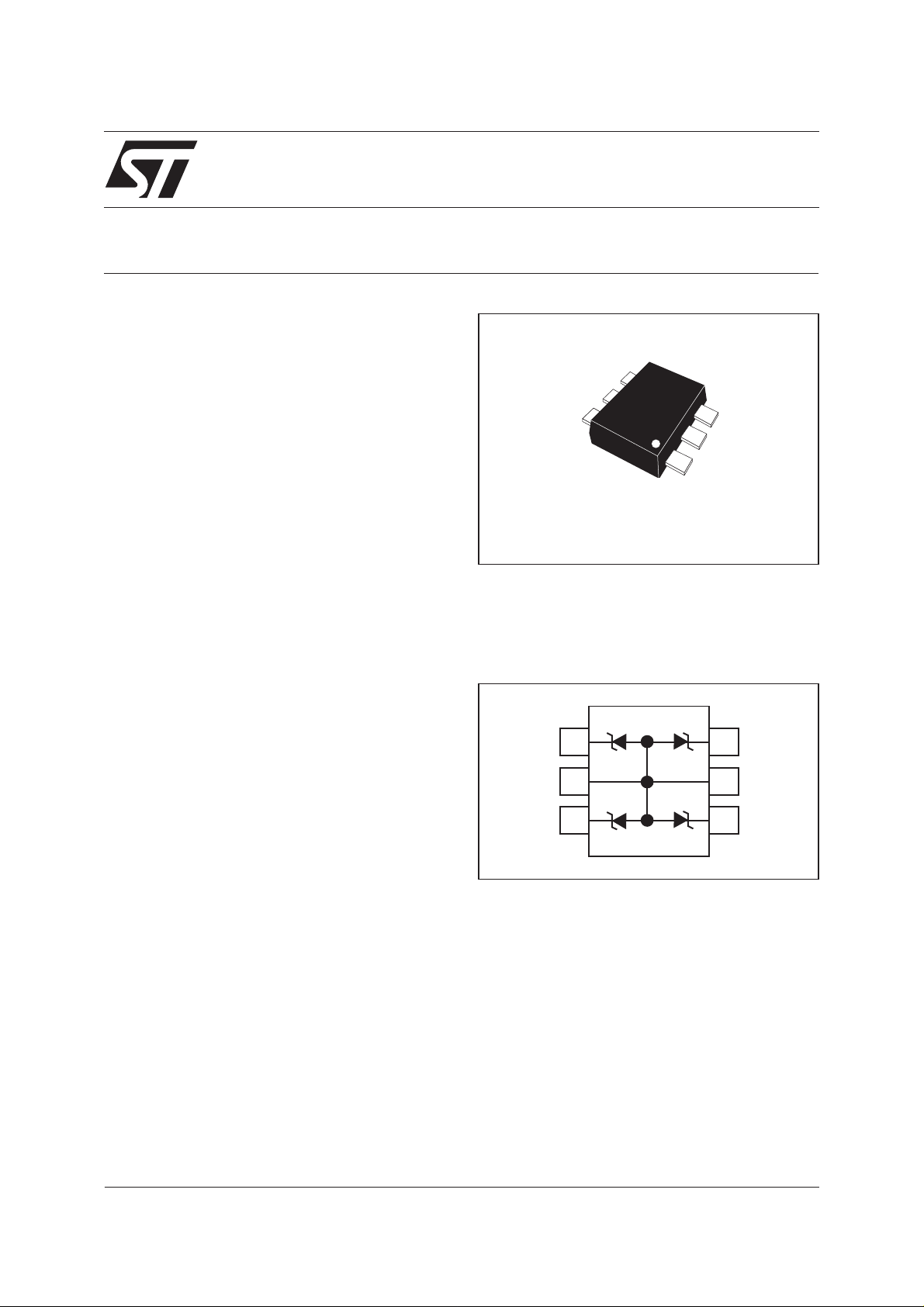
The ESDA6V1P6 is a monolithic array designed to
protect up to 4 lines against ESD transients.
This device is ideal for applications where board
space saving is required.
= 6.1V MIN
BR
2
QUAD TRANSIL™ ARRAY
FOR ESD PROTECTION
SOT-666
FUNCTIONAL DIAGRAM
1
6
BENEFITS
■
High ESD protection level.
■
High integration.
■
Suitable for high density boards.
COMPLIESWITH THE FOLLOWING STANDARDS:
■
IEC61000-4-2 level 4: 15 kV (air discharge)
8kV (contact discharge)
■
MIL STD 883E-Method 3015-7: class 3
25kV HBM (Human Body Model)
January 2003 - Ed: 2
2
3
5
4
1/8
Page 2
ESDA6V1P6
ABSOLUTE RATINGS (T
amb
= 25°C)
Symbol Parameter Test conditions Value Unit
V
PP
P
PP
T
j
T
stg
T
L
T
op
Note 1: for a surge greater than the maximum values, the diode will fail in short-circuit.
ESD discharge - IEC61000-4-2 air discharge
IEC61000-4-2 contact discharge
Peak pulse power (8/20 µs) (see note 1) Tjinitial = Tamb
Junction temperature
Storage temperature range
Maximum lead temperature for soldering during 10s at 5mm for case
Operating temperature range
±15
±8
150 W
125 °C
-55to+150 °C
260 °C
-40to+150 °C
THERMAL RESISTANCES
Symbol Parameter Value Unit
R
th(j-a)
ELECTRICAL CHARACTERISTICS (T
Junction to ambient on printed circuit on recommended pad layout
= 25°C)
amb
220 °C/W
kV
Symbol Parameter
V
RM
V
BR
V
CL
I
RM
I
PP
αT
V
F
C
R
d
Types V
ESDA6V1P6
Stand-off voltage
Breakdown voltage
Clamping voltage
Leakage current
Peak pulse current
Voltage tempature coefficient
Forward voltage drop
Capacitance per line
Dynamic resistance
BR
min. max. max. typ. max. typ.
VVmAµAV
6.1 7.2 1 0.5 3 1.5 4.5 70
@I
R
V
CLVBRVRM
Slope: 1/R
IRM@V
RM
I
I
F
V
F
I
RM
d
I
PP
Rd αTC
@0V
Ω10
-4
/°C pF
V
2/8
Page 3
ESDA6V1P6
Fig. 1: Relative variation of peak pulse power
versus initial junction temperature.
P [T initial] / P [T initial=25°C)
PP j PP j
1.1
1.0
0.9
0.8
0.7
0.6
0.5
0.4
0.3
0.2
0.1
0.0
0 25 50 75 100 125 150
T (°C)
j
Fig. 3: Clamping voltage versus peak pulse
current (typical values, rectangular waveform).
I (A)
PP
100.0
t =2.5µs
p
T initial=25°C
j
Fig. 2:Peak pulse power versusexponentialpulse
duration.
P (W)
PP
1000
100
T (µs)
10
1 10 100
p
T initial=25°C
j
Fig. 4: Forward voltage drop versus peak forward
current (typical values).
I (A)
FM
1.E+00
10.0
1.0
V (V)
0.1
0 10203040506070
CL
Fig. 5: Junction capacitance versus reverse
voltage applied (typical values).
C(pF)
80
70
60
50
40
30
20
10
0
0123456
V (V)
R
F=1MHz
V =30mV
OSC RMS
T=25°C
j
T=125°C
1.E-01
1.E-02
1.E-03
0.0 0.2 0.4 0.6 0.8 1.0 1.2 1.4 1.6 1.8 2.0
j
T=25°C
j
V (V)
FM
Fig. 6: Relative variation of leakage current versus
junction temperature (typical values).
I [T ] / I [T =25°C]
Rj Rj
2.0
V =3V
R
1.8
1.6
1.4
1.2
1.0
0.8
0.6
0.4
0.2
0.0
25 50 75 100 125
T (°C)
j
3/8
Page 4

ESDA6V1P6
TECHNICAL INFORMATION
1. ESD protection by ESDA6V1P6
Fig. A1: Application example.
With the focus of lowering the operation levels, the
problemofmalfunction caused by theenvironment
is critical. Electrostatic discharge (ESD) is a major
cause of failure in electronic systems.
I/O2
I/O1
As a transient voltage suppressor, ESDA6V1P6 is
an ideal choice for ESD protection by suppressing
ESD events. It is capable of clamping the
Connector
incoming transient to a low enough level such that
any damage is prevented on the device protected
by ESDA6V1P6.
ESDA6V1P6 serves as a parallel protection
elements, connected between the signal line and
ground. As the transient rises above the operating
voltage of the device, the ESDA6V1P6 becomesa
low impedance path diverting the transient current
to ground.
The clamping voltage is given by the following formula:
=VBR+Rd.I
V
CL
PP
As shown in figure A2, the ESD strikes are clamped by the transient voltage suppressor.
Fig. A2: ESD clamping behavior.
I/O4
I/O3
IC
to be
protected
R
G
V
G
I
PP
R
d
V(i/o)
V
BR
R
LOAD
Device
to be
ESD surge ESD6V1P6
Tohave a good approximationofthe remaining voltages atboth Vi/o side, weprovidethe typical dynamical
resistance value R
we have:
The results ofthecalculationdone V
= 1.5Ω (typ.) give:
R
d
This confirms the very low remaining voltage across the device to be protected. It is also important to note
that in this approximation the parasitic inductance effect was not taken into account. This could be a few
tenths of volts during a few ns at the Vi/o side.
. By taking into account the following hypothesis:
d
R
Vi o V R
()
= 8kV, RG= 330Ω(IEC61000-4-2 standard), VBR= 6.4V (typ.)and
G
V i o Volts
()
and R
G>Rd
/ =+×
load>Rd
BR d
/.=42 8
V
R
g
g
protected
4/8
Page 5

ESDA6V1P6
Fig. A3: ESD test board.
± 15kV ESD
Air discharge
V(i/o)
Fig. A5: Remaining voltage during ESD surge.
Fig. A4: ESD test configuration.
I/O1, I/O2, I/O3 or I/O4
± 15kV ESD
Air discharge
GND
V(i/o)
a: Response in the positive way b: Response in the negative way
2. Crosstalk behavior
Fig. A6: Crosstalk phenomenon
RG1
G1
V
RG2
VG2
DRIVERS RECEIVERS
Line 1
Line 2
R
L1
R
L2
αβ
αβ
V+ V
1G1 12G2
V+ V
2G2 21G1
5/8
Page 6

ESDA6V1P6
Thecrosstalkphenomena are due to the coupling between 2lines.Coupling factors ( β12 or β21 ) increase
whenthe gap across linesdecreases, particularly insilicondice. In theexample above, the expectedsignal
on load R
signal represents the effect of the crosstalk phenomenon of the line 1 on the line 2. This phenomenon has
to be taken into account when the drivers impose fast digital data or high frequency analog signals. The
perturbed line will be more affected if it works with low voltage signal or high load impedance (few kΩ)
is α2VG2, in facttherealvoltageatthis point has got an extra value β21VG2. This partoftheV
L2
G1
Fig. A7: Analog crosstalk test configuration.
I/O1
I/O4
unloaded
GND
50Ω
Port 2
VG
50Ω
Port 1
Fig. A9: Digital crosstalk test configuration.
I/O1
unloaded
Fig. A8: Typical analog crosstalk response.
I/O1
I/O4
unloaded
GND
50Ω
Port 2
VG
50Ω
Port 1
Fig. A10: Typical digital crosstalk response.
0 - 5V
pulse generator
F= 100KHz
R
t = 20ns
6/8
G1
V
GND
β21 G1V
crosstalk
V
β
21 G1
unloaded
I/O4
Page 7

ESDA6V1P6
3. PCB layout recommendations
As ESD is a fast event, the di/dt caused by this surge is about 30A/ns (risetime=1ns, Ipeak=30A), that
means each nH causes an overvoltage of 30V.
Thus, the circuit board layout is a critical design step in the suppression of ESD induced transients by
reducing parasitic inductances. To ensure that, the following guidelines are recommended :
The ESDA6V1P6 should be placed as close as possible to the input terminals or connectors.
■
The path length between the ESD suppressor and the protected line should be minimized.
■
All conductive loops, including power and ground loops should be minimized.
■
The ESD transient return path to ground should be kept as short as possible.
■
The connections from the ground pins to the ground plane should be the shortest possible.
■
4. Comparison with varistors
Varistors TRANSIL™
Leakage current
Protection efficiency
Ageing
Low leakage current for Transil™ device
Improve the autonomy of portable equipments as mobile
■
Better efficiency in terms of ESD protection by using Transil™ device
■ Varistors are bidirectional devices and so are not suitable to protect sensitive ICs, because they will be
submitted to high voltages in the negative way.
■ Ratio V
■
Less dispersion in terms of V
CL/VBR
lower for Transil™ device
BR
No ageing phenomena regarding ESD events with Transil™ device
■
Higher efficiency in terms of ESD protection
-- +++
-- ++
-- ++
ORDER CODE
ESDA 6V1 P6
ESD ARRAY
V min
BR
Ordering type Marking Package Weight Base qty Delivery mode
ESDA6V1P6 B SOT-666 2.9 mg. 3000 Tape & reel
PACKAGE:SOT-666
7/8
Page 8

ESDA6V1P6
PACKAGE MECHANICAL DATA
SOT-666
DIMENSIONS
bp
D
A
FOOT PRINT (in millimeters)
0.36
REF.
Millimeters Inches
Min. Max. Min. Max.
A 0.50 0.60 0.020 0.024
bp 0.17 0.27 0.007 0.011
e1
e
E
c 0.08 0.18 0.003 0.007
D 1.50 1.70 0.060 0.067
E 1.10 1.30 0.043 0.051
e 1.00 0.040
e1 0.50 0.020
Lp
He
U
He 1.50 1.70 0.059 0.067
Lp 0.10 0.30 0.004 0.012
0.30
0.84
0.20 0.20
Informationfurnished is believed to beaccurateand reliable. However, STMicroelectronics assumesno responsibility for the consequencesof
useof such information norforany infringement of patentsor other rights of thirdparties which may resultfromits use. No licenseis granted by
implication or otherwise under any patent or patent rights of STMicroelectronics. Specifications mentioned in this publication are subject to
change without notice. This publication supersedes and replaces all information previously supplied.
STMicroelectronics products are not authorized for use as critical components in life support devices or systems without express written approval of STMicroelectronics.
0.62
2.30
The ST logo is a registered trademark of STMicroelectronics
© 2003 STMicroelectronics - Printed in Italy - All rights reserved.
STMicroelectronics GROUP OF COMPANIES
Australia - Brazil - Canada - China - Finland - France - Germany
Hong Kong - India - Israel - Italy - Japan - Malaysia - Malta - Morocco - Singapore
Spain - Sweden - Switzerland - United Kingdom - United States.
http://www.st.com
8/8
 Loading...