

Page 1
®
ESDA6V1BC6
Application Specific Discretes
A.S.D.
APPLICATIONS
Where transient overvoltage protection in ESD
sensitive equipment is required, such as :
COMPUTERS
■
PRINTERS
■
COMMUNICATION SYSTEMS
■
VIDEO EQUIPMENT
■
Thisdeviceisparticularlyadaptedtotheprotection
of symmetrical signals.
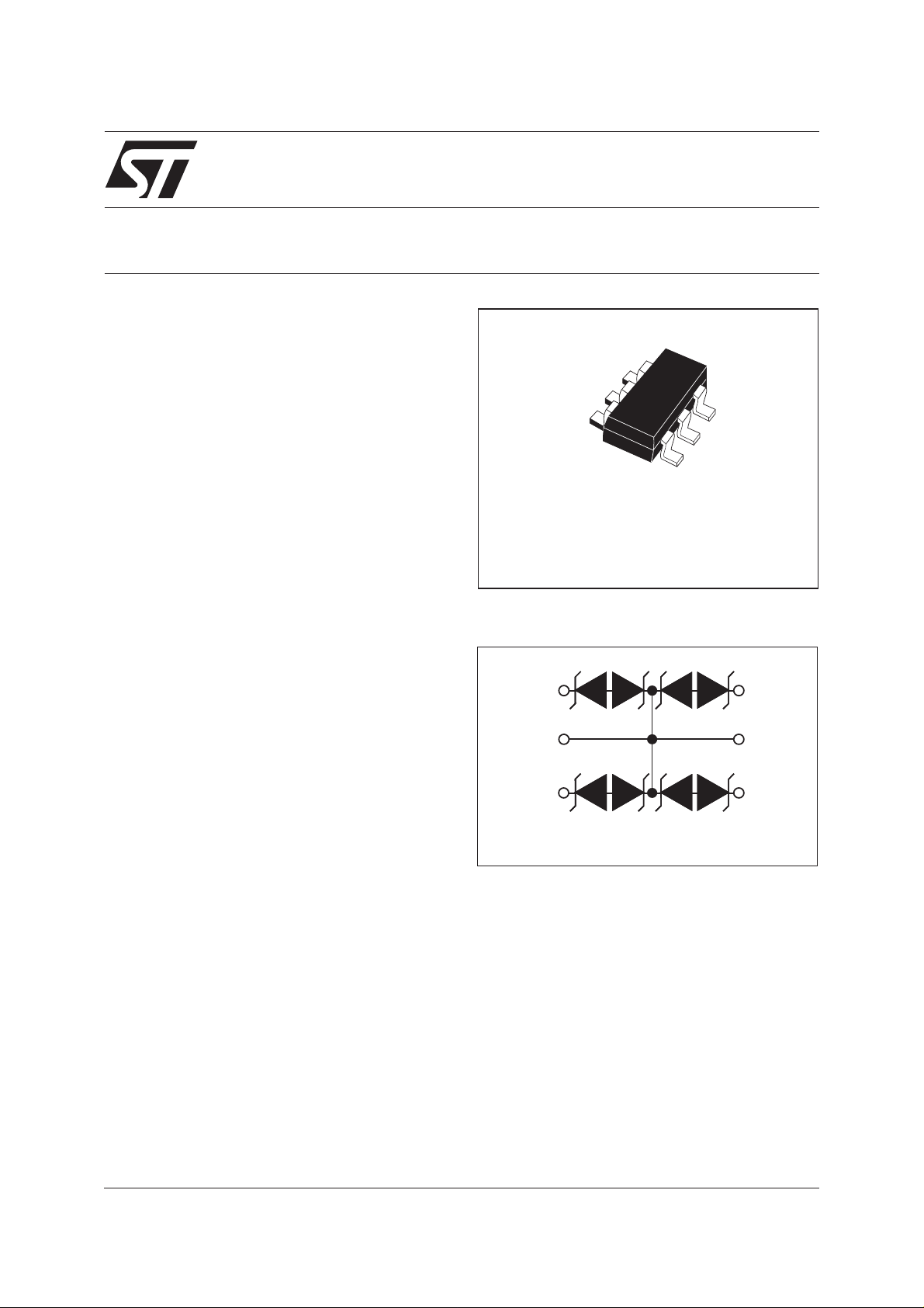
DESCRIPTION
The ESDA6V1BC6 is a monolithic array designed
to protect up to 4 lines in a bidirectional way
against ESD transients.
The device is ideal for situations where board
space is at a premium.
FEATURES
■ 4 BIDIRECTIONAL TRANSIL FUNCTIONS
■
ESD PROTECTION FOR DATA, SIGNAL AND
BUS
V
CC
■
STAND OFF VOLTAGE RANGE: ± 5 V MIN.
■
LOW LEAKAGE CURRENT < 1 µA
■
PEAK PULSE POWER ( 8/20)=80W
SUPPRESSOR FOR ESD PROTECTION
QUAD BIDIRECTIONAL TRANSIL
SOT23-6L (SC-74)
FUNCTIONAL DIAGRAM
SOT23-6L
1
2
3
6
5
4
BENEFITS
■
High ESD protection level : up to 25 kV
■
High integration
■
Suitable for high density boards
COMPLIES WITH THE FOLLOWING STANDARDS:
- IEC61000-4-2: 15 kV (air discharge)
8 kV (contact discharge)
- MIL STD 883C-Method 3015-6: class3
(human body model)
January 2002 - Ed: 1C
1/6
Page 2
ESDA6V1BC6
1. ESD protection by ESDA6V1BC6
With the focus of lowering the operation levels, the problem of malfunction caused by the environment is
critical. Electrostatic discharge (ESD) is a major cause of failure in electronic system.
Transient Voltage Suppressors are an ideal choice for ESD protection and have proven capable in
suppressing ESD events. They are capable of clamping the incoming transient to a low enough level such
that damage to the protected semiconductor is prevented.
Surface mount TVS arrays offer the best choice for minimal lead inductance.
They serve as parallel protection elements, connected between the signal line to ground. As the transient
risesabove the operating voltageofthe device, theTVSarray becomes a lowimpedance path diverting the
transient current to ground.
Bidirectional protection for 0V biased signals.
DRIVER
CONNECTOR
The ESDA6V1BC6 array is the ideal product for use as board level protection of ESD sensitive
semiconductor components.
The tiny SOT23-6L package allows design flexibility in the design of “crowded” boards where the space
saving is at a premium. This enables to shorten the routing and can contribute to improve ESD
performance.
2. Circuit Board Layout
Circuit board layout is a critical design step in the suppression of ESD induced transients. The following
guidelines are recommended :
■
The ESDA6V1BC6 should be placed as near as possible to the input terminals or connectors.
■
Minimise the path length between the ESD suppressor and the protected device
■
Minimise all conductive loops, including power and ground loops
■
The ESD transient return path to ground should be kept as short as possible.
■
Use ground planes whenever possible.
2/6
Page 3

ESDA6V1BC6
ABSOLUTE MAXIMUM RATINGS (T
amb
= 25°C)
Symbol Test conditions Value Unit
V
PP
P
PP
T
j
T
stg
T
L
T
op
Note 1: Variation of parameters is given by curves.
ELECTRICAL CHARACTERISTICS (T
Symbol Parameter
V
RM
V
BR
V
CL
I
RM
ESD discharge - MILSTD 883C - Method 3015-6
IEC61000-4-2 air discharge
IEC61000-4-2 contact discharge
Peak pulse power (8/20µs)
Junction temperature
Storage temperature range
Lead solder temperature (10 second duration)
Operating temperature range (note 1)
= 25°C)
amb
Stand-off voltage
Breakdown voltage
Clamping voltage
V
V
CL
Leakage current
BR
25
15
8
80 W
150 °C
-55 to +150 °C
260 °C
-40 to +125 °C
I
V
RM
I
RM
kV
V
I
PP
C
Rd
Peak pulse current
Capacitance
Dynamic resistance
Type
ESDA6V1BC6
Note 1 : Square pulse, Ipp = 3A, tp=2.5µs.
V
@IRIRM@V
BR
Rd
RM
I
PP
Rd αTC
min. max. max. typ. max. typ.
note 1 0V bias
-4
VVmAµAV Ω 10
/°C pF
6.181151.35 3 20
3/6
Page 4

ESDA6V1BC6
Fig. 1: Peak power dissipation versus initial
junction temperature.
Ppp[Tj initial]/Pp p [T j in itia l= 2 5 °C]
1.1
1.0
0.9
0.8
0.7
0.6
0.5
0.4
0.3
0.2
0.1
0.0
0 25 50 75 100 125 150 175
Tj initial(°C)
Fig. 3: Clamping voltage versus peak pulse
current (Tj initial = 25 °C).
Rectangular waveform tp = 2.5 µs.
Ipp(A)
20.0
tp=2.5µs
10.0
1.0
0.1
0 5 10 15 20 25 30 35 40
Vcl(V)
Fig. 2: Peakpulse power versus exponential pulse
duration (Tj initial = 25 °C).
Ppp(W)
500
100
10
1 10 100
tp(µs)
Fig. 4: Capacitance versus reverse applied
voltage (typical values).
C(pF)
22
21
20
19
18
17
16
15
14
13
12
11
10
012345678
VR(V)
F=1MHz
Vosc=30mV
Fig. 5: Relative variation of leakage current versus
junction temperature (typical values).
IR[Tj] / IR[Tj=25°C ]
500
100
10
1
25 50 75 100 125 150
4/6
Tj(°C)
Page 5

ORDER CODE
ESD ARRAY
ESDA6V1BC6
ESDA 6V1 B C6
PACKAGE:
C6: SOT23-6L (SC-74)
PACKAGE MECHANICAL DATA
SOT23-6L
E
e
D
e
C
θ
H
A1
L
b
V min.
BR
A
A2
Bidirectional
REF. DIMENSIONS
Millimeters Inches
Min. Typ. Max. Min. Typ. Max.
A 0.90 1.45 0.035 0.057
A1 0 0.10 0 0.004
A2 0.90 1.30 0.035 0.0512
b 0.35 0.50 0.0137 0.02
c 0.09 0.20 0.004 0.008
D 2.80 3.00 0.11 0.118
E 1.50 1.75 0.059 0.0689
e 0.95 0.0374
H 2.60 3.00 0.102 0.118
L 0.10 0.60 0.004 0.024
θ 10° 10°
FOOTPRINT
3.50
0.138
2.30
0.090
mm
inch
0.95
0.037
0.60
0.024
1.10
0.043
1.20
0.047
MARKING
Type Marking
ESDA6V1BC6 BS55
Packaging: Standard packaging is tape and reel.
5/6
Page 6

ESDA6V1BC6
Informationfurnished is believed tobe accurate and reliable.However, STMicroelectronics assumes noresponsibility for the consequencesof
useof such informationnor for any infringementof patents or other rights of thirdparties which may result from its use.No license is grantedby
implication or otherwise under any patent or patent rights of STMicroelectronics. Specifications mentioned in this publication are subject to
change without notice. This publication supersedes and replaces all information previously supplied.
STMicroelectronics products are not authorized for use as critical components in life support devices or systems without express written approval of STMicroelectronics.
The ST logo is a registered trademark of STMicroelectronics
© 2002 STMicroelectronics - Printed in Italy - All rights reserved.
STMicroelectronics GROUP OF COMPANIES
Australia - Brazil - Canada - China - Finland - France - Germany
Hong Kong - India - Israel - Italy - Japan - Malaysia - Malta - Morocco - Singapore
Spain - Sweden - Switzerland - United Kingdom - United States.
http://www.st.com
6/6
 Loading...