

Page 1
®
ESDA6V1-5W6
Application Specific Discretes
A.S.D.
APPLICATIONS
Where transient overvoltage protection in ESD
sensitive equipment is required, such as :
Computers
n
Printers
n
Communication systems
n
Cellular phone handsets and accessories
n
Other telephone sets
n
Set top boxes
n
DESCRIPTION
The ESDA6V1-5W6 is a 5-bit wide monolithic
suppressor which is designed to protect
components connected to data and transmission
lines against ESD.
FEATURES
n
5 UNIDIRECTIONAL TRANSIL FUNCTIONS
n
BREAKDOWN VOLTAGE: VBR = 6.1V min
n
LOW LEAKAGE CURRENT: IRmax<1µA
n
VERYSMALL SIZEFOR PCBSPACE SAVING:
4.2mm
2
TYPICALLY
ä
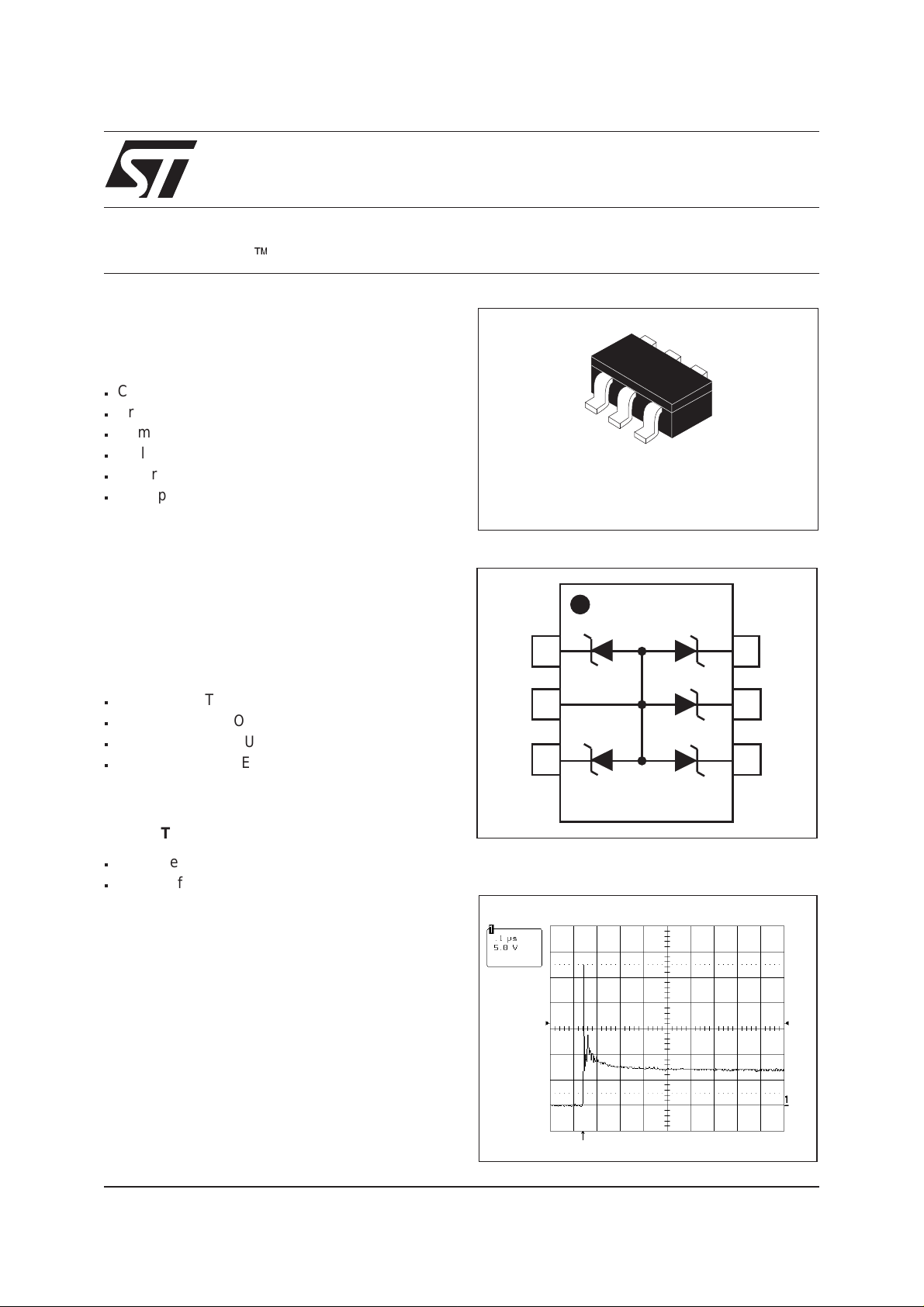
TRANSIL ARRAY
FOR ESD PROTECTION
SOT323-6L
FUNCTIONAL DIAGRAM
I/O1
Gnd
I/O2
I/O5
I/O4
I/O3
BENEFITS
n
High integration
n
Suitable for high density boards
COMPLIES WITH THE FOLLOWING STANDARDS:
- IEC 61000-4-2: level 4
15 kV (air discharge)
8 kV (contact discharge)
- MIL STD 883C-Method 3015-6: class3
(human body model)
March 2000 -Ed: 1A
ESD response to IEC61000-4-2
(air discharge 16kV, positive surge)
1/9
Page 2
ESDA6V1-5W6
ABSOLUTE MAXIMUM RATINGS (T
amb
= 25°C)
Symbol Test conditions Value Unit
V
PP
P
PP
T
j
T
stg
T
L
T
op
Note 1: The evolution of the operating parameters versus temperature is given by curves and αT parameter.
ELECTRICAL CHARACTERISTICS (T
ESD discharge - MIL STD 883C - Method 3015-6
IEC 61000-4-2 air discharge
IEC 61000-4-2 contact discharge
Peak pulse power (8/20µs)
Junction temperature
Storage temperature range
Lead solder temperature (10 seconds duration)
Operating temperature range (note 1)
= 25°C)
amb
25
20
15
100 W
150 °C
-55 to +150 °C
260 °C
-40 to +125 °C
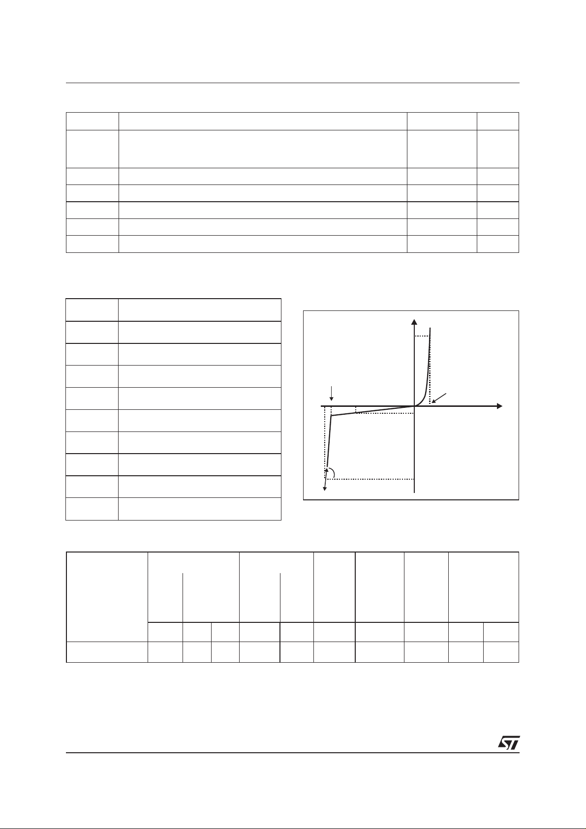
Symbol Parameter
I
V
RM
V
BR
V
CL
I
RM
I
PP
Stand-off voltage
Breakdown voltage
Clamping voltage
Leakage current
Peak pulse current
Vcl
VBR
IF
VF
VRM
IRM
kV
V
αT
C
Rd
V
F
Voltage temperature coefficient
Capacitance
Dynamic impedance
Forward voltage drop
V
BR@IR
min. max
Type
.
VVmAµAVmΩ10
ESDA6V1-5W6
Note 2 : Square pulse, Ipp = 15A, tp=2.5µs.
Note 3: ∆VBR= αT*(T
6.1 7.2 1 1 3 610 6 50 1.25 200
- 25°C) * VBR(25°C)
amb
Slope = 1/Rd
IPP
IRM@V
RM
Rd αTCV
max. typ. max. typ. max
note 2 note 3 0V bias
-4
/°C pF V mA
F@IF
2/9
Page 3
ESDA6V1-5W6
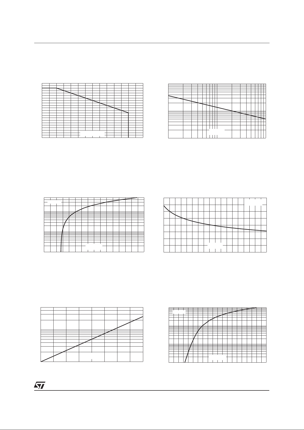
Fig. 1: Peak power dissipation versus initial
junction temperature.
Ppp[Tj initial]/Pp p [T j in itia l= 2 5 °C]
1.1
1.0
0.9
0.8
0.7
0.6
0.5
0.4
0.3
0.2
0.1
0.0
0 25 50 75 100 125 150 175
Tj initial(°C)
Fig. 3: Clamping voltage versus peak pulse current
(Tj initial = 25°C) Rectangular waveform tp = 2.5µs.
Ipp(A)
50.0
tp=2.5µs
10.0
Fig. 2: Peak pulse power versus exponential
pulse duration (Tj initial = 25°C).
Ppp(W)
1000
100
tp(µs)
10
1 10 100
Fig. 4: Capacitance versus reverse applied voltage
(typical values).
C(pF)
50
40
F=1MHz
Vosc=30mV
1.0
Vcl(V)
0.1
0 5 10 15 20 25 30 35 40
Fig. 5: Relative variation of leakage current versus junction temperature (typical values).
IR[Tj] / IR[Tj=25°C]
50
10
Tj(°C)
1
25 50 75 100 125
30
20
VR(V)
10
0.5 1.0 1.5 2.0 2.5 3.0 3.5 4.0 4.5 5.0
Fig. 6: Peak forward voltage drop versus peak
forward current (typical values).
IFM(A)
1E+0
1E-1
1E-2
1E-3
Tj=25°C
VFM(V)
0.6 0.7 0.8 0.9 1.0 1.1 1.2 1.3 1.4 1.5 1.6
3/9
Page 4

APPLICATION EXAMPLE
Connector
Implementation of ESDA6V1-5W6 in a typical application
ESDA6V1-5W6
IC to be protected
TECHNICAL INFORMATION
ESD PROTECTION
The ESDA6V1-5W6 is particularly optimized to perform ESD protection. ESD protection is achieved by
clamping the unwanted overvoltage. The clamping voltage is given by the following formula :
VVRI
cl br d pp
=+⋅
As shown in figure A1, the ESD strikes are clamped by the transient voltage suppressor.
Fig. A1: ESD clamping behavior
Rg
Rd
Vg
Voutput
Vbr
Rload
ESD Surge
4/9
ESDA6V1-5W6
Device
to be
protected
Page 5

ESDA6V1-5W6
Tohave agood approximationof theremaining voltagesat bothVi/o side,we providethe typicaldynamical
resistance value Rd. By taking into account the following hypothesis :
Rg > Rd and Rload > Rd
we have:
g
Vin V R
br d
=+×
The results of the calculation done for Vg = 8 kV, Rg = 330 Ω (IEC 61000-4-2 standard), Vbr = 6.4 V (typ.)
and Rd = 0.61 Ω (typ.) give:
Vouput = 21.2 V
This confirms the very low remaining voltage across the device to be protected. It is also important to note
that in this approximation the parasitic inductance effect was not taken into account. This could be a few
tenths of volts during a few ns at the Vi/o side.
Fig. A2: Measurement conditions:
V
R
g
ESD
SURGE
16kV
Air
Discharge
TEST BOARD
E62
Vi/o
5/9
Page 6

ESDA6V1-5W6
The measurements done here after show very clearly (Fig. A3) the high efficiency of the ESD protection:
theclamping voltageVout becomesvery closeto Vbr(positive way,Fig. A3a)and -Vf(negative way,Fig.
A3b).
Fig. A3: Remaining voltage during ESD surge
a: Vi/o during positive surge
b: Vi/o during negative surge
Onecan note thatthe ESDA6V1-5W6is notonly acting forpositive ESDsurges butalso for negative ones.
For these kind of disturbances it clamps close to ground voltage as shown in Fig. A3b.
CROSSTALK BEHAVIOR
Fig. A4: Crosstalk phenomenon
R
G1
Line 1
V
G1
R
G2
R
L1
αβ
V+ V
1G1 12G2
Line 2
V
G2
R
L2
V+ V
αβ
2G2 21G1
6/9
DRIVERS
RECEIVERS
Page 7

ESDA6V1-5W6
The crosstalk phenomena are due to the coupling between 2 lines. The coupling factor ( β12or β21)
increases when the gap across lines decreases, particularly in silicon dice. In the example above the
expected signal on load R
Thispart ofthe V
signalrepresents theeffect ofthe crosstalkphenomenon ofthe line1 onthe line2. This
G1
phenomenon has to be taken into account when the drivers impose fast digital data or high frequency
analog signals in the disturbing line. The perturbed line will be more affected if it works with low voltage
signal or high load impedance (few kΩ).
Fig. A5: Analog crosstalk measurements
50
Port1
Vg
is α2VG1. In fact the real voltage at this point has got an extra value β21VG1.
L2
TEST BOARD
Ω
E62
Port2
50
Ω
Fig. A6: Typical analog crosstalk measurements
Analog crosstalk (dB)
0
-20
-40
-60
-80
-100
1 10 100 1,000
frequency (MHz)
Figure A5 gives themeasurement circuitfor the analogcrosstalk application.In figure A6, the curveshows
the effect of the cell I/O5 on the cell I/O3. In usual frequency range of analog signals (up to 100MHz) the
effect on disturbed line is less than -40dB.
7/9
Page 8

ESDA6V1-5W6
Fig. A7: Digital crosstalk measurements configuration
+5V +5V
74HC04
Line1
V
G1
Square
Pulse
Generator
Fig. A8: Digital crosstalk measurements configuration
+5V
Line 2
ESDA6V1
-5W6
β
21 G1
74HC04
V
Figure A7 shows the measurement circuit used to quantify the crosstalk effect in a classical digital
application.
Figure A8 shows that in such acondition, i.e signalfrom 0 to5V and risetime of afew ns, the impact on the
disturbed line isless than 50 mV peak to peak.No data disturbance was noted on the concerned line. The
measurements performed with falling edges give an impact within the same range.
ORDER CODE
ESDA 6V 1 - 5 W6
BR
Vmin
ESD ARRAY
5 lines protected
8/9
SOT323-6L
Page 9

PACKAGE MECHANICAL DATA
SOT323-6L
A
A1
H
ESDA6V1-5W6
DIMENSIONS
A2
D
ee
REF.
Millimeters Inches
Min. Max. Min. Max.
A 0.8 1.1 0.031 0.043
A1 0 0.1 0 0.004
A2 0.8 1 0.031 0.039
b 0.15 0.3 0.006 0.012
c 0.1 0.18 0.004 0.007
D 1.8 2.2 0.071 0.086
E
E 1.15 1.35 0.045 0.053
e 0.65Typ. 0.025Typ.
Q
c
b
H 1.8 2.4 0.071 0.094
Q 0.1 0.4 0.004 0.016
FOOT PRINT
0.3mm
1mm
2.9mm
1mm
0.35mm
MARKING
Type Marking Package Weight Base Qty Delivery mode
ESDA6V1-5W6 E62 SOT323-6L 5.4 mg 3000 Tape & Reel
Informationfurnishedisbelievedtobeaccurate and reliable. However, STMicroelectronics assumes no responsibility for the consequences of
useofsuchinformationnorforanyinfringementofpatentsorotherrightsofthirdpartieswhichmayresultfrom its use. No license is granted by
implication or otherwise under any patent or patent rights of STMicroelectronics. Specifications mentioned in this publication are subject to
change without notice. This publication supersedes and replaces all information previously supplied.
STMicroelectronics products are not authorized for use as critical components in life support devices or systems without express written approval of STMicroelectronics.
The ST logo is a registered trademark of STMicroelectronics
© 2000 STMicroelectronics - Printed in Italy - All rights reserved.
STMicroelectronics GROUP OF COMPANIES
Australia - Brazil - China - Finland - France - Germany - Hong Kong - India - Italy - Japan - Malaysia
Malta - Morocco - Singapore - Spain - Sweden - Switzerland - United Kingdom - U.S.A.
http://www.st.com
9/9
 Loading...