

Page 1
®
ESDA6V1-5SC6
Application Specific Discretes
A.S.D.
APPLICATIONS
Where transient overvoltage protection in ESD
sensitive equipment is required, such as :
Computers
■
Printers
■
Communication systems
■
Cellular phone handsets and accessories
■
Other telephone sets
■
Set top boxes
■
DESCRIPTION
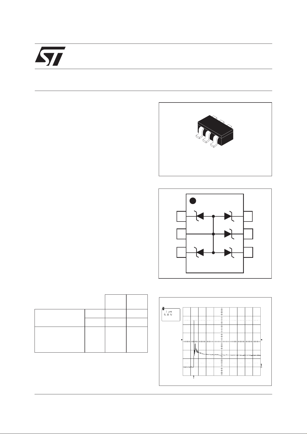
The ESDA6V1-5SC6 is a 5-bit wide monolithic
suppressor which is designed to protect against
ESD components connected to data and
transmission lines.
FEATURES
■ 5 UNIDIRECTIONAL TRANSIL FUNCTIONS
■
BREAKDOWN VOLTAGE: VBR = 6.1V min
■
LOW LEAKAGE CURRENT: IRmax<1µA
TRANSIL ARRAY
FOR ESD PROTECTION
SOT23-6L
FUNCTIONAL DIAGRAM
I/O1
Gnd
I/O5
I/O4
BENEFITS
■
High integration
■
Suitable for high density boards
COMPLIES WITH THE FOLLOWING STANDARDS:
Max
current
IEC 61000-4-2
level 4
MIL STD
Test kV
Air 15 Contact 8 30 A
Contact > 4 > 2.67 A
883C-Method
3015.7 class3
(human body model)
February 2002 -Ed: 2B
I/O2
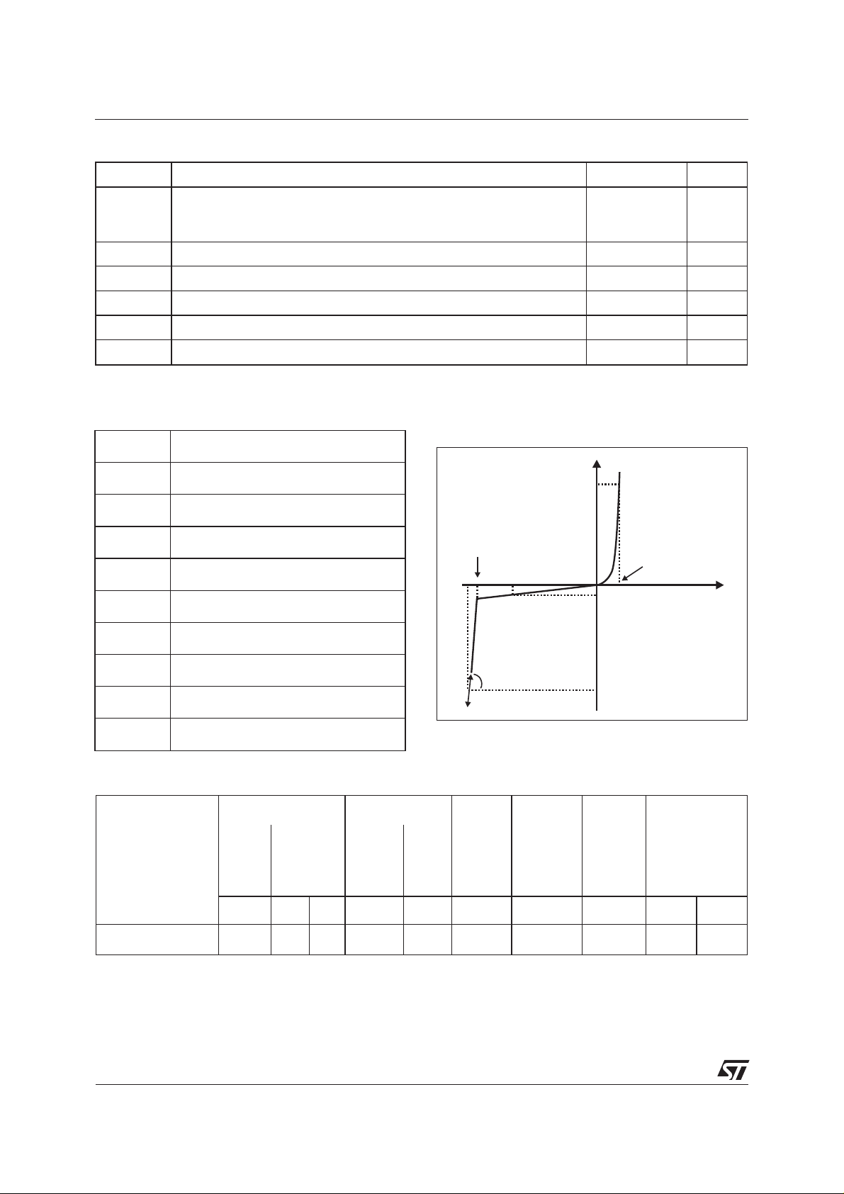
ESD response to IEC61000-4-2
(air discharge 16kV, positive surge)
I/O3
1/5
Page 2
ESDA6V1-5SC6
ABSOLUTE MAXIMUM RATINGS (T
amb
= 25°C)
Symbol Test conditions Value Unit
V
PP
P
PP
T
j
T
stg
T
L
T
op
Note 1: The evolution of the operating parameters versus temperature is given by curves and αT parameter.
ELECTRICAL CHARACTERISTICS (T
ESD discharge - MIL STD 883E - Method 3015-7
IEC 61000-4-2 air discharge
IEC 61000-4-2 contact discharge
Peak pulse power (8/20µs)
Junction temperature
Storage temperature range
Lead solder temperature (10 seconds duration)
Operating temperature range (note 1)
= 25°C)
amb
25
20
15
100 W
150 °C
-55 to +150 °C
260 °C
-40 to +125 °C
Symbol Parameter
I
V
RM
V
BR
V
CL
I
RM
I
PP
Stand-off voltage
Breakdown voltage
Clamping voltage
Leakage current
Peak pulse current
Vcl
VBR
IF
VF
VRM
IRM
kV
V
αT
C
Rd
V
F
Voltage temperature
Capacitance
Dynamic impedance
Forward voltage drop
V
BR@IR
min. max
Type
VVmAµAVmΩ10
ESDA6V1-5SC6
Note 2 : Square pulse, Ipp = 15A, tp=2.5µs.
Note 3: ∆VBR= αT*(T
6.1 7.2 1 1 3 590 6 50 1.25 200
- 25°C) * VBR(25°C)
amb
Slope = 1/Rd
IPP
IRM@V
RM
Rd αTCV
F@IF
max. typ. max. typ. max
.
note 2 note 3 0V bias
-4
/°C pF V mA
2/5
Page 3

ESDA6V1-5SC6
Fig. 1: Peak power dissipation versus initial
junction temperature.
Ppp[Tj initial]/Pp p [T j in itia l= 2 5 °C]
1.1
1.0
0.9
0.8
0.7
0.6
0.5
0.4
0.3
0.2
0.1
0.0
0 25 50 75 100 125 150 175
Tj initial(°C)
Fig. 3: Clamping voltage versus peak pulse current
(Tj initial = 25°C) Rectangular waveform tp = 2.5µs.
Ipp(A)
50.0
tp=2.5µs
10.0
Fig. 2: Peak pulse power versus exponential
pulse duration (Tj initial = 25°C).
Ppp(W)
1000
100
tp(µs)
10
1 10 100
Fig. 4: Capacitance versus reverse applied voltage
(typical values).
C(pF)
50
40
F=1MHz
Vosc=30mV
1.0
Vcl(V)
0.1
0 5 10 15 20 25 30 35 40
Fig. 5: Relative variation of leakage current versus junction temperature (typical values).
IR[Tj] / IR[Tj=25°C]
50
10
Tj(°C)
1
25 50 75 100 125
30
20
VR(V)
10
0.5 1.0 1.5 2.0 2.5 3.0 3.5 4.0 4.5 5.0
Fig. 6: Peak forward voltage drop versus peak
forward current (typical values).
IFM(A)
1E+0
1E-1
1E-2
1E-3
Tj=25°C
VFM(V)
0.6 0.7 0.8 0.9 1.0 1.1 1.2 1.3 1.4 1.5 1.6
3/5
Page 4

ESDA6V1-5SC6
PACKAGE MECHANICAL DATA
SOT23-6L
e
D
e
C
FOOT PRINT
A
E
A2
REF. DIMENSIONS
Millimeters Inches
Min. Typ. Max. Min. Typ. Max.
A 0.90 1.45 0.035 0.057
b
A1 0 0.10 0 0.004
A2 0.90 1.30 0.035 0.0512
b 0.35 0.50 0.0137 0.02
c 0.09 0.20 0.004 0.008
D 2.80 3.00 0.11 0.118
E 1.50 1.75 0.059 0.0689
e 0.95 0.0374
θ
H
A1
L
0.60
0.024
H 2.60 3.00 0.102 0.118
L 0.10 0.60 0.004 0.024
θ 10° 10°
3.50
0.138
2.30
0.090
mm
inch
0.95
0.037
1.10
0.043
1.20
0.047
4/5
Page 5

ESDA6V1-5SC6
ORDER CODE
ESDA 6V1 - 5 SC6
BR
V min
ESD ARRAY
5 lines protected
MARKING
Type Marking Package Weight Base Qty Delivery mode
ESDA6V1-5SC6 EC62 SOT23-6L 16.7 mg 3000 Tape & Reel
SOT23-6L
Informationfurnishedisbelievedto be accurate and reliable. However, STMicroelectronics assumes no responsibility fortheconsequencesof
useofsuchinformationnorforany infringement of patents or other rights of third parties which may result from its use. Nolicenseisgrantedby
implication or otherwise under any patent or patent rights of STMicroelectronics. Specifications mentioned in this publication are subject to
change without notice. This publication supersedes and replaces all information previously supplied.
STMicroelectronics products are not authorized for use as critical components in life support devices or systems without express written approval of STMicroelectronics.
The ST logo is a registered trademark of STMicroelectronics
© 2002 STMicroelectronics - Printed in Italy - All rights reserved.
STMicroelectronics GROUP OF COMPANIES
Australia - Brazil - Canada - China - Finland - France - Germany
Hong Kong - India - Israel - Italy - Japan - Malaysia - Malta - Morocco - Singapore
Spain - Sweden - Switzerland - United Kingdom - United States.
http://www.st.com
5/5
 Loading...