

Page 1

ESDAxxSC5
®
ESDAxxSC6
Application Specific Discretes
A.S.D.™
APPLICATIONS
Where transient overvoltage protection in ESD
sensitive equipment is required, such as :
- Computers
- Printers
- Communication systems
- Cellular phone handsets and accessories
- Other telephone set
- Set top boxes
FEATURES
4 Unidirectional Transil™ Functions
■
Low leakage current: IRmax. < 20 µAatV
■
■ 500 W Peak pulse power (8/20 µs)
DESCRIPTION
The ESDAxxSC5 and ESDAxxSC6 are monolithic
voltage suppressors designed to protect
components which are connected to data and
transmission lines against ESD.
They clamp the voltage just above the logic level
supply for positive transients, and to a diode drop
below ground for negative transient.
BR
QUAD TRANSIL ARRAY
FOR ESD PROTECTION
SOT23-5L (SC-59)
ESDAxxSC5
FUNCTIONAL DIAGRAM
SOT23-5L
1
2
3
SOT23-6L (SC-59)
ESDAxxSC6
5
4
BENEFITS
High ESD protection level : up to 25 kV
High integration
Suitable for high density boards
COMPLIES WITH THE FOLLOWING STANDARDS:
IEC61000-4-2 : level 4
15kV (air discharge)
8kV (contact discharge)
MIL STD 883E-Method 3015-7 : class3B
(human body model)
May 2002 Ed: 6F
SOT23-6L
1
2
3
6
5
4
1/9
Page 2
ESDAxxSC5 / ESDAxxSC6
ABSOLUTE MAXIMUM RATINGS (T
amb
= 25°C)
Symbol Test conditions Value Unit
V
PP
ESD discharge - MIL STD 883E - Method 3015-7
25 kV
IEC61000-4-2 air discharge
IEC61000-4-2 contact discharge
P
PP
Peak pulse power (8/20µs) note1 ESDA5V3SCx
500 W
ESDA6V1SCx
ESDA14V2SCx
300 W
ESDA17SC6
ESDA19SC6
ESDA25SC6
T
j
T
stg
T
L
T
op
Junction temperature
Storage temperature range
Lead solder temperature (10 second duration)
Operating temperature range
ELECTRICAL CHARACTERISTICS (T
Symbol Parameter
V
V
V
I
I
αT
RM
BR
CL
RM
PP
Stand-off voltage
Breakdown voltage
Clamping voltage
Leakage current
Peak pulse current
Voltage temperature coefficient
amb
= 25°C)
I
I
F
V
BR
V
V
CL
RM
150 °C
-55 to +150 °C
260 °C
-40 to +125 °C
V
F
I
RM
V
2/9
C
Rd
V
Capacitance
Dynamic resistance
F
Forward voltage drop
Rd
I
PP
Page 3
V
@IRIRM@V
BR
ESDAxxSC5 / ESDAxxSC6
Rd αTCV
RM
@I
F
F
Types
min. max. max. typ. max. typ. max.
VVmAµAVmΩ10
ESDA5V3SC5
5.3 5.9 1 2 3 230 5 280 1.25 200
ESDA5V3SC6
ESDA6V1SC5
6.1 7.2 1 20 5.25 350 6 190 1.25 200
ESDA6V1SC6
ESDA14V2SC5
14.2 15.8 1 5 12 650 10 100 1.25 200
ESDA14V2SC6
ESDA17SC6
ESDA19SC6
ESDA25SC6
note 1 : Square pulse, Ipp = 15A, tp=2.5µs.
note 2 : ∆ VBR= αT* (Tamb -25°C) * VBR(25°C)
17
19
19
21
1
0.075
1
0.1
25 30 1 1 24 1000 10 60 1.2 10
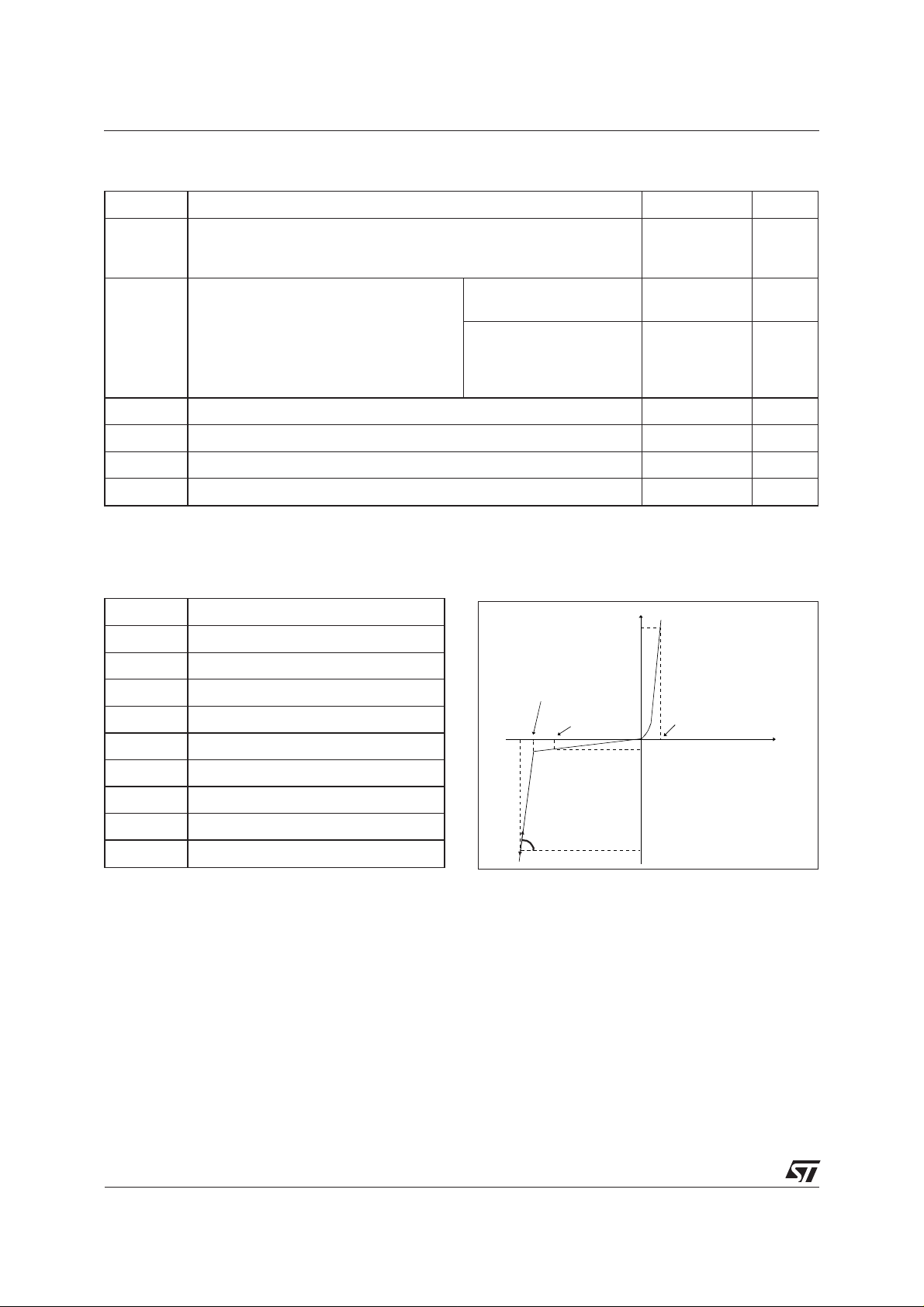
CALCULATION OF THE CLAMPING VOLTAGE
USE OF THE DYNAMIC RESISTANCE
The ESDA familyhasbeendesignedto clamp fast
spikes like ESD. Generally the PCB designers
need to calculate easily the clamping voltage V
CL
This is why we give the dynamic resistance in
addition to the classical parameters. The voltage
across the protection cell can be calculated with
the following formula:
VCL=VBR+RdI
PP
note 1 note 2 0V bias
-4
/°C pF V mA
14
15
700
800
10
8.5
85
80
1.2
1.2
As the value of the dynamic resistance remains
stable for a surge duration lower than 20µs, the
2.5µs rectangular surge is well adapted. In
.
addition both rise and fall times are optimized to
avoid any parasitic phenomenon during the
measurement of Rd.
10
10
WhereIpp is thepeakcurrent through theESDA cell.
DYNAMIC RESISTANCE MEASUREMENT
The short duration of the ESD has led us to prefer
amore adapted test wave, asbelow defined, to the
classical 8/20µs and 10/1000µs surges.
I
Ipp
2µs
tp = 2.5µs
s duration measurement wave.
2.5
t
3/9
Page 4

ESDAxxSC5 / ESDAxxSC6
Fig. 1: Peak power dissipation versus initial
junction temperature.
Ppp [Tj initial] / Ppp [Tj initial=25°C]
1.1
1.0
0.9
0.8
0.7
0.6
0.5
0.4
0.3
0.2
0.1
0.0
0 25 50 75 100 125 150
Tj initial(°C)
Fig. 3: Clamping voltage versus peak pulse
current (Tj initial = 25 °C).
Rectangular waveform (tp = 2.5 µs).
Ipp(A)
50.0
10.0
1.0
ESDA6V1SC5/SC6
ESDA5V3SC5/SC6
ESDA19SC6
ESDA17SC6
ESDA14V2SC5/SC6
Vcl(V)
0.1
0 5 10 15 20 25 30 35 40 45 50 55 60 65 70 75 80
ESDA25SC6
tp=2.5µs
Fig. 2: Peakpulse power versus exponential pulse
duration (Tj initial = 25 °C).
Ppp(W)
5000
ESDA5V3SC5/SC6
&
ESDA6V1SC5/SC6
1000
ESDA14V2SC5/SC6
ESDA17SC6
ESDA19SC6
ESDA25SC6
tp(µs)
100
1 10 100
Fig. 4: Capacitance versus reverse applied
voltage (typical values).
C(pF)
500
ESDA5V3SC5/SC6
100
ESDA6V1SC5/SC6
ESDA14V2SC5/SC6
VR(V)
10
12 51020 50
ESDA17SC6
ESDA19SC6
F=1MHz
Vosc=30mV
ESDA25SC6
Fig. 5: Relative variation of leakage current versus
junction temperature (typical values).
IR[Tj] / IR[Tj=25°C]
500
ESDA14V2SC5/SC6
100
&
ESDA6V1SC5/SC6
10
Tj(°C)
1
25 50 75 100 125
4/9
ESDA17SC6
&
ESDA19SC6
ESDA5V3SC5/SC6
ESDA25SC6
Fig. 6: Peak forward voltage drop versus peak
forward current (typical values).
IFM(A)
5.00
1.00
0.10
0.01
ESDA5V3SC5/SC6
ESDA14V2SC5/SC6
&
ESDA6V1SC5/SC6
ESDA19SC6
ESDA17SC6
ESDA25SC6
VFM(V)
0.5 1.0 1.5 2.0 2.5 3.0 3.5 4.0
Page 5

ESD protection by ESDAXXXSCX
Electrostatic discharge (ESD) is a major cause of
failure in electronic systems.
Transient Voltage Suppressors (TVS) are an ideal
choice for ESD protection. They are capable of
clamping the incoming transient overvoltage to a
low enough level such that damage to the
protected semiconductor is prevented.
Surfacemount TVSarrays offer the best choice for
minimal lead inductance.
I/ O LINES
ESDAxxSC5 / ESDAxxSC6
They serve as parallel protection elements,
connected between the signal line and ground. As
the transient rises above the operating voltage of
the device, the TVS array becomes a low
impedance path diverting the transient current to
ground.
ESD
sensitive
device
ESDAxxxSC6 (1connection to GND for ESDAxxSC5)
The ESDAxxSCx array is the ideal board level
protection of ESD sensitive semiconductor
components.
Thetiny SOT23-5L and SOT23-6L packagesallow
design flexibility in the high density boards where
the space saving is at a premium. This enables to
shorten the routing and contributes to hardening
against ESD.
ADVICE FOR OPTIMIZING CIRCUIT BOARD
LAYOUT
Circuit board layout is a critical design step in the
suppression of ESD induced transients. The
following guidelines are recommended :
■
TheESDAxxSC5/6 should beplaced as closeas
possible to the input terminals or connectors.
GND
■
The path length between the ESD suppressor
and the protected line should be minimized
■
All conductive loops, including power and
ground loops should be minimized
■
The ESD transient return path to ground should
be kept as short as possible.
■
Ground planes should be used whenever possible.
5/9
Page 6

ESDAxxSC5 / ESDAxxSC6
ADVICE FOR OPTIMIZING CIRCUIT BOARD LAYOUT
Circuit board layout is a critical design step in the suppression of ESD induced transients. The following
guidelines are recommended:
The ESDA19SC6 should be placed as close as possible to the input terminals or connectors.
■
The path length between the ESD suppressor and the protected line should be minimized.
■
All conductive loops, including power and ground loops should be minimized.
■
The ESD transient return path to ground should be kept as short as possible.
■
Ground planes should be used whenever possible.
■
TECHNICAL INFORMATION
ESD PROTECTION
The ESDA19SC6 is particularly optimized to perform ESD protection. ESD protection is achieved by
clamping the unwanted overvoltage. The clamping voltage is given by the following formula :
VVRI
=+⋅
CL BR
As shown in figure A1, the ESD strikes are clamped by the transient voltage suppressor.
dpp
Fig. A1: ESD clamping behavior (example)
Rg
Rd
Vg
Voutput
BR
V
Rload
Device
to be
ESD Surge
ESDA19SC6
protected
To have a good approximation of the remaining voltages at both VI/O side, we provide the typical
dynamical resistance value Rd. By taking into account the following hypothesis :
Rg > Rd and Rload > Rd
we have:
V
VOutput V R
=+×
BR
g
d
R
g
The results of the calculation done for Vg = 8 kV, Rg = 330 Ω (IEC61000-4-2 standard), Vbr = 19 V (typ.)
and Rd = 0.80 Ω (typ.) give:
VOuput = 38.4 V
This confirms the very low remaining voltage across the device to be protected. It is also important to note
that in this approximation the parasitic inductance effect was not taken into account. This could be a few
tenths of volts during a few nanoseconds at the output side.
6/9
Page 7

ORDER CODE
ESDAxxSC5 / ESDAxxSC6
ESDA 6V1 SC6
ESD ARRAY
PACKAGE:
SC5: SOT23-5L
V min
BR
ORDERING INFORMATION
Odering Type Marking Package Weight Base qty Delivery mode
ESDA5V3SC5 EC53 SOT23-5L 16.7 mg 3000 Tape & reel
ESDA5V3SC6 ES53 SOT23-6L 16.7 mg 3000 Tape & reel
ESDA6V1SC5 EC61 SOT23-5L 16.7 mg 3000 Tape & reel
ESDA6V1SC6 ES61 SOT23-6L 16.7 mg 3000 Tape & reel
ESDA14V2SC5 EC15 SOT23-5L 16.7 mg 3000 Tape & reel
ESDA14V2SC6 ES15 SOT23-6L 16.7 mg 3000 Tape & reel
ESDA17SC6 ES17 SOT23-6L 16.7 mg 3000 Tape& reel
ESDA19SC6 ES19 SOT23-6L 16.7 mg 3000 Tape& reel
ESDA25SC6 ES25 SOT23-6L 16.7 mg 3000 Tape& reel
■
Epoxy meets UL94-V0 standard
SC6: SOT23-6L
7/9
Page 8

ESDAxxSC5 / ESDAxxSC6
PACKAGE MECHANICAL DATA
SOT23-5L
e
D
e
C
FOOT PRINT
A
E
A2
REF.
Millimeters Inches
DIMENSIONS
Min. Typ. Max. Min. Typ. Max.
A 0.90 1.45 0.035 0.057
A1 0 0.10 0 0.004
b
A2 0.90 1.30 0.035 0.0512
b 0.35 0.50 0.0137 0.02
c 0.09 0.20 0.004 0.008
D 2.80 3.00 0.11 0.118
E 1.50 1.75 0.059 0.0689
e 0.95 0.0374
θ
H
A1
L
H 2.60 3.00 0.102 0.118
L 0.10 0.60 0.004 0.024
θ 10° 10°
0.95
0.037
0.60
0.024
3.50
0.138
2.30
0.090
1.20
0.047
mm
inch
1.10
0.043
8/9
Page 9

PACKAGE MECHANICAL DATA
SOT23-6L
ESDAxxSC5 / ESDAxxSC6
e
D
e
C
FOOT PRINT
A
E
A2
REF.
Millimeters Inches
Min. Typ. Max. Min. Typ. Max.
A 0.90 1.45 0.035 0.057
A1 0 0.10 0 0.004
DIMENSIONS
b
A2 0.90 1.30 0.035 0.0512
b 0.35 0.50 0.0137 0.02
c 0.09 0.20 0.004 0.008
D 2.80 3.00 0.11 0.118
E 1.50 1.75 0.059 0.0689
e 0.95 0.0374
θ
H
A1
L
H 2.60 3.00 0.102 0.118
L 0.10 0.60 0.004 0.024
θ 10° 10°
0.60
0.024
1.20
0.047
3.50
2.30
0.138
0.090
Informationfurnishedisbelievedtobeaccurate and reliable. However, STMicroelectronicsassumes no responsibility for theconsequences of
useof such information nor forany infringement of patents or other rights of third parties which may result from its use. No license is granted by
implication or otherwise under any patent or patent rights of STMicroelectronics. Specifications mentioned in this publication are subject to
change without notice. This publication supersedes and replaces all information previously supplied.
STMicroelectronics products are not authorized for use as critical components in life support devices or systems without express written approval of STMicroelectronics.
mm
inch
1.10
0.043
0.95
0.037
The ST logo is a registered trademark of STMicroelectronics
© 2002 STMicroelectronics - Printed in Italy - All rights reserved.
STMicroelectronics GROUP OF COMPANIES
Australia - Brazil - Canada - China - Finland - France - Germany
Hong Kong - India - Israel - Italy - Japan - Malaysia - Malta - Morocco - Singapore
Spain - Sweden - Switzerland - United Kingdom - United States.
http://www.st.com
9/9
 Loading...