

Page 1
®
ESDA17/19-5SC6
Application Specific Discretes
A.S.D.™
APPLICATIONS
Where transient overvoltage protection in ESD
sensitive equipment is required, such as :
Computers
■
Printers and other peripherals
■
Communications systems
■
Cellular phone handsets and accessories
■
Other telephone sets
■
Consumer Electronics (Set top boxes, DVD
■
players, TV sets)
DESCRIPTION
The ESDA17/19-5SC6 is a monolithic array
designed to protect up to 5 lines against ESD
transients.
The device is ideal for applications where board
space savind is required.
TRANSIL™ ARRAY
FOR ESD PROTECTION
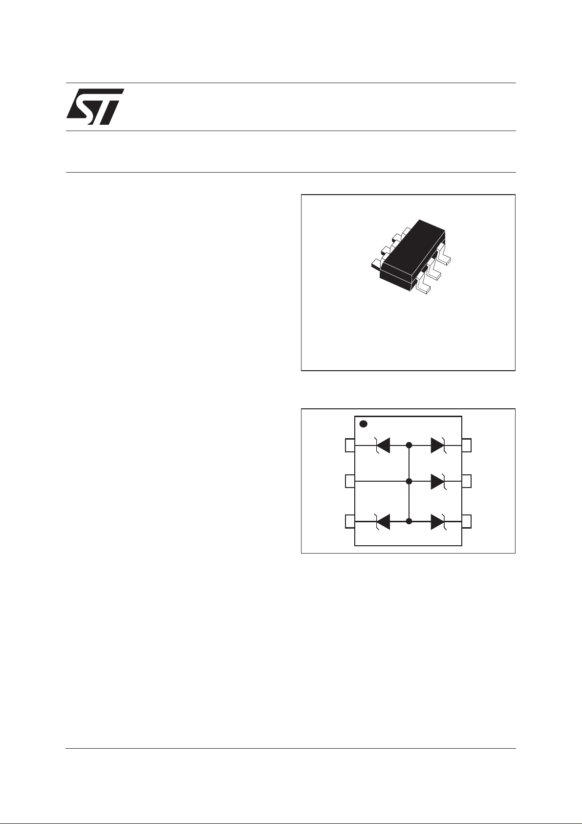
SOT23-6L
ESDAxx-5SC6
FUNCTIONAL DIAGRAM
SOT23-6L
FEATURES
■
5 Unidirectional transil™ functions
■
Minimumbreakdown voltagerange v
BRmin
=17V
or 19V
■
Peak pulse power (8/20µs); 150W
■
Tiny leakage current at stand-off voltage: <
100nA
BENEFITS
■
High ESD protection level
■
High integration
■
Suitable for high density boards
COMPLIES WITH THE FOLLOWING STANDARDS:
- IEC61000-4-2: 15 kV (air discharge)
8 kV (contact discharge)
- MIL STD 883E-Method 3015-7: class3
25kV (human body model)
I/O1
Gnd
I/O2
I/O5
I/O4
I/O3
November 2002 -Ed: 1A
1/5
Page 2
ESDA17/19-5SC6
ABSOLUTE MAXIMUM RATINGS (T
amb
= 25°C)
Symbol Test conditions Value Unit
V
PP
P
PP
ESD discharge - IEC61000-4-2 air discharge
IEC61000-4-2 contact discharge
Peak pulse power dissipation (8/20µs)
Tj initial = Tamb
±15
±8
150 W
Note 1
T
j
T
stg
T
L
Junction temperature
Storage temperature range
Maximum lead temperature for soldering during 10s at 5mm for
125 °C
-55 to +150 °C
260 °C
case
T
op
Note 1: For a surge greater than the maximum values, the diode will fail in short-circuit.
ELECTRICAL CHARACTERISTICS (T
Operating temperature range
= 25°C)
amb
Symbol Parameter
V
V
V
I
RM
I
PP
αT
V
RM
BR
CL
F
Stand-off voltage
Breakdown voltage
Clamping voltage
Leakage current @ V
RM
Peak pulse current
Voltage temperature coefficient
Forward voltage drop
V
CL
V
BR
V
RM
Rd
-40 to +125 °C
I
I
F
VF
I
RM
I
PP
kV
V
V
@IRIRM@V
BR
Type
min. max. max. typ. max.
V V mA nA V Ω 10
ESDA17-5SC6
ESDA19-5SC6
Note 1 : Square pulse, Ipp = 15A, tp=2.5µs.
Note 2: ∆ VBR= αT* (Tamb-25°C) * VBR(25°C)
17 19 1 75 14 1 10 33 1.2 10
19 21 1 100 15 1 8.5 33 1.2 10
RM
Rd αTCV
note 1 note 2 0V bias
-4
/°C pF V mA
F@IF
2/5
Page 3

ESDA17/19-5SC6
Fig. 1: Relative variation of peak pulse power
versus initial junction temperature.
PP PP
P [Tj initial] / P [Tj initial = 25°C]
1.1
1.0
0.9
0.8
0.7
0.6
0.5
0.4
0.3
0.2
0.1
0.0
0 25 50 75 100 125 150
Tj (°C)
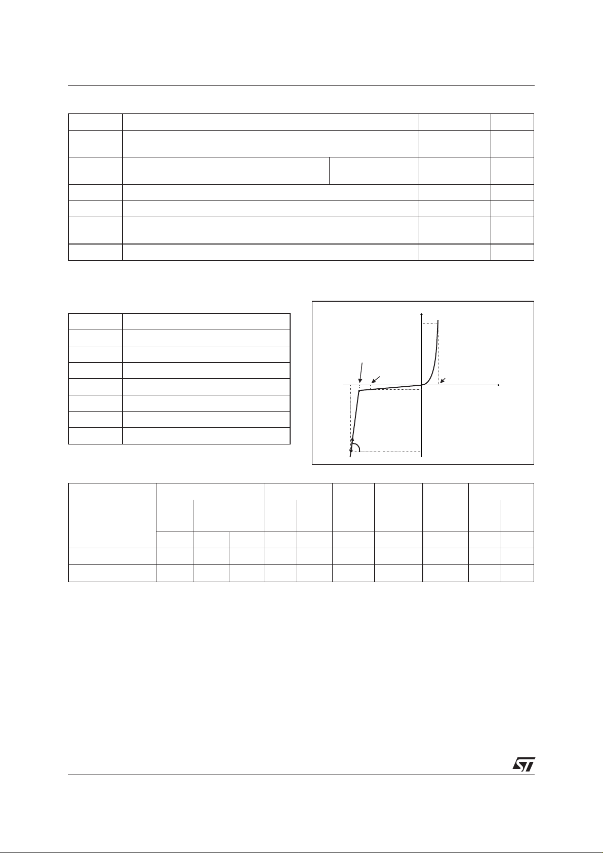
Fig. 3: Clamping voltage versus peak pulse
current (typical values, rectangular waveform).
I (A)PP
100.0
Fig. 2: Peak pulse power versus exponential pulse
duration.
P (W)PP
1000
100
Tjinitial = 25°C
tp (µs)
10
1 10 100
Fig. 4: Forward voltage drop versus peak forward
current (typical values).
I (A)FM
1.E+00
10.0
ESDA17-5SC6
1.0
0.1
0 10203040506070
ESDA19-5SC6
V (V)CL
tP=2.5µs
T
initial =25°C
j
Fig. 5: Junction capacitance versus reverse voltage applied (typical values).
C(pF)
40
35
30
25
20
15
10
5
0
01234567891011121314151617
V (V)R
V
F=1MHz
osc
Tj=25°C
=30mV
RMS
1.E-01
1.E-02
Tj=125°C
Tj=25°C
V (V)FM
1.E-03
0.0 0.2 0.4 0.6 0.8 1.0 1.2 1.4 1.6 1.8 2.0
Fig. 6: Relative variationof leakage current versus
junction temperature (typical values).
IR [Tj] / IR [Tj = 25°C]
100
VR=14V
10
Tj(°C)
1
25 50 75 100 125
3/5
Page 4

ESDA17/19-5SC6
ORDER CODE
ESDA 17 - 5 SC6
PACKAGE:
ESD ARRAY
V min.
BR
5 lines protected
OTHER INFORMATIONS
Type Marking Package Weight Base Qty Delivery mode
ESDA17-5SC6 175 SOT23-6L 16.7mg 3000 Tape & Reel
ESDA19-5SC6 195 SOT23-6L 16.7mg 3000 Tape & Reel
Epoxy meets UL94, V0
■
SC6: SOT23-6L
4/5
Page 5

PACKAGE MECHANICAL DATA
SOT23-6L
ESDA17/19-5SC6
e
D
e
C
FOOTPRINT
A
E
A2
REF. DIMENSIONS
Millimeters Inches
Min. Typ. Max. Min. Typ. Max.
A 0.90 1.45 0.035 0.057
A1 0 0.10 0 0.004
b
A2 0.90 1.30 0.035 0.0512
b 0.35 0.50 0.0137 0.02
c 0.09 0.20 0.004 0.008
D 2.80 3.00 0.11 0.118
E 1.50 1.75 0.059 0.0689
e 0.95 0.0374
H 2.60 3.00 0.102 0.118
θ
H
A1
L
0.60
0.024
L 0.10 0.60 0.004 0.024
θ 10° 10°
1.20
0.047
3.50
2.30
0.138
0.090
Informationfurnishedis believed to be accurate and reliable. However, STMicroelectronics assumes no responsibility for the consequencesof
useofsuchinformation nor for any infringement of patents or other rights of third parties which may result from its use. No license is granted by
implication or otherwise under any patent or patent rights of STMicroelectronics. Specifications mentioned in this publication are subject to
change without notice. This publication supersedes and replaces all information previously supplied.
STMicroelectronics products are not authorized for use as critical components in life support devices or systems without express written approval of STMicroelectronics.
mm
inch
0.95
0.037
1.10
0.043
The ST logo is a registered trademark of STMicroelectronics
© 2002 STMicroelectronics - Printed in Italy - All rights reserved.
STMicroelectronics GROUP OF COMPANIES
Australia - Brazil - Canada - China - Finland - France - Germany
Hong Kong - India - Israel - Italy - Japan - Malaysia - Malta - Morocco - Singapore
Spain - Sweden - Switzerland - United Kingdom - United States.
http://www.st.com
5/5
 Loading...