

Page 1
ESD11N5.0ST5G
Transient Voltage
Suppressors
Micro−Packaged Diodes for ESD Protection
The ESD11N is designed to protect voltage sensitive components
that require ultra−low capacitance from ESD and transient voltage
events. Excellent clamping capability, low capacitance, low leakage,
and fast response time, make these parts ideal for ESD protection on
designs where board space is at a premium. Because of its low
capacitance, it is suited for use in high frequency designs such as USB
2.0 high speed and antenna line applications.
http://onsemi.com
Specification Features
• Low Capacitance 0.6 pF
• Low Clamping Voltage
• Small Body Outline Dimensions: 0.60 mm x 0.30 mm
• Low Body Height: 0.3 mm
• Stand−off Voltage: 5.0 V
• Low Leakage
• Response Time is < 1 ns
• IEC61000−4−2 Level 4 ESD Protection
• These Devices are Pb−Free, Halogen Free/BFR Free and are RoHS
Compliant
Mechanical Characteristics
MOUNTING POSITION:
QUALIFIED MAX REFLOW TEMPERATURE: 260°C
Device Meets MSL 1 Requirements
MAXIMUM RATINGS
Rating Symbol Value Unit
IEC 61000−4−2 (ESD) Contact
Total Power Dissipation on FR−5 Board
(Note 1) @ T
Thermal Resistance, Junction−to−Ambient
Junction and Storage Temperature Range TJ, T
Lead Solder Temperature − Maximum
(10 Second Duration)
Stresses exceeding Maximum Ratings may damage the device. Maximum
Ratings are stress ratings only. Functional operation above the Recommended
Operating Conditions is not implied. Extended exposure to stresses above the
Recommended Operating Conditions may affect device reliability.
1. FR−5 = 1.0 x 0.75 x 0.62 in.
= 25°C
A
Any
Air
°PD°
R
q
T
JA
−40 to +125 °C
stg
L
±8.0
±15
250
400
260 °C
mW
°C/W
kV
MARKING
DIAGRAM
PIN 1
DSN2
CASE 152AA
XXXX = Specific Device Code
YYY = Year Code
ORDERING INFORMATION
Device Package Shipping
ESD11N5.0ST5G DSN2
(Pb−Free)
†For information on tape and reel specifications,
including part orientation and tape sizes, please
refer to our Tape and Reel Packaging Specifications
Brochure, BRD8011/D.
XXXX
YYY
†
5000/Tape & Reel
See Application Note AND8308/D for further description of survivability specs.
© Semiconductor Components Industries, LLC, 2010
October, 2010 − Rev. 4
1 Publication Order Number:
ESD11N5.0S/D
Page 2
ESD11N5.0ST5G
ELECTRICAL CHARACTERISTICS
(TA = 25°C unless otherwise noted)
Symbol
V
I
PP
V
RWM
I
V
I
Maximum Reverse Peak Pulse Current
Clamping Voltage @ I
C
Working Peak Reverse Voltage
Maximum Reverse Leakage Current @ V
R
Breakdown Voltage @ I
BR
Test Current
T
*See Application Note AND8308/D for detailed explanations of
Parameter
PP
RWM
T
BR
V
RWM
VCV
Bi−Directional TVS
I
I
PP
I
T
I
R
I
V
RWM
V
R
I
T
I
PP
BR
V
V
C
datasheet parameters.
ELECTRICAL CHARACTERISTICS (T
Device
Device
Marking
= 25°C unless otherwise noted)
A
V
RWM
(V)
I
R
@ V
(mA)
RWM
VBR (V) @ I
(Note 2)
T
I
T
C (pF)
Max Max Min mA Typ Max
VC (V) @
= 1 A
I
PP
Max
(Note 3)
V
C
Per IEC61000−4−2
(Note 4)
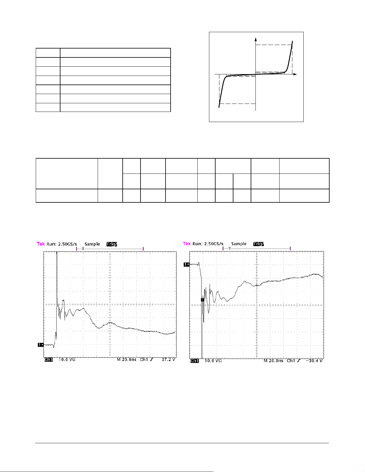
ESD11N5.0ST5G N5S0 5.0 1.0 5.8 1.0 0.6 0.9 12 Figures 1 and 2
See Below
2. VBR is measured with a pulse test current IT at an ambient temperature of 25°C.
3. Surge current waveforms per Figure 5.
4. For test procedure see Figures 3 and 4 and Application Note AND8307/D.
Figure 1. ESD Clamping Voltage Screenshot
Positive 8 kV Contact per IEC61000−4−2
http://onsemi.com
Figure 2. ESD Clamping Voltage Screenshot
Negative 8 kV Contact per IEC61000−4−2
2
Page 3
ESD11N5.0ST5G
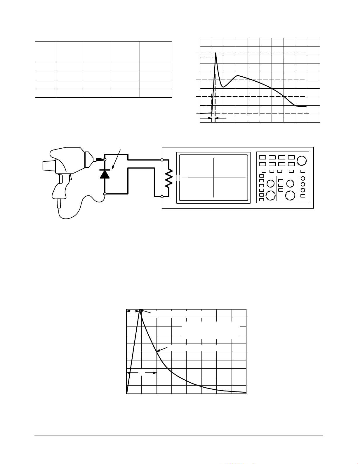
IEC 61000−4−2 Spec.
Test
Voltage
Level
1 2 7.5 4 2
2 4 15 8 4
3 6 22.5 12 6
4 8 30 16 8
(kV)
ESD Gun
First Peak
Current
(A)
Current at
30 ns (A)
TVS
50 W
Cable
IEC61000−4−2 Waveform
I
peak
Current at
60 ns (A)
100%
90%
I @ 30 ns
I @ 60 ns
10%
Figure 3. IEC61000−4−2 Spec
Oscilloscope
50 W
tP = 0.7 ns to 1 ns
Figure 4. Diagram of ESD Test Setup
The following is taken from Application Note
AND8308/D − Interpretation of Datasheet Parameters
for ESD Devices.
ESD Voltage Clamping
For sensitive circuit elements it is important to limit the
voltage that an IC will be exposed to during an ESD event
to as low a voltage as possible. The ESD clamping voltage
is the voltage drop across the ESD protection diode during
an ESD event per the IEC61000−4−2 waveform. Since the
IEC61000−4−2 was written as a pass/fail spec for larger
100
t
r
90
80
70
60
50
40
30
20
% OF PEAK PULSE CURRENT
10
0
020406080
PEAK VALUE I
t
P
Figure 5. 8 X 20 ms Pulse Waveform
systems such as cell phones or laptop computers it is not
clearly defined in the spec how to specify a clamping voltage
at the device level. ON Semiconductor has developed a way
to examine the entire voltage waveform across the ESD
protection diode over the time domain of an ESD pulse in the
form of an oscilloscope screenshot, which can be found on
the datasheets for all ESD protection diodes. For more
information on how ON Semiconductor creates these
screenshots and how to interpret them please refer to
AND8307/D.
@ 8 ms
RSM
PULSE WIDTH (tP) IS DEFINED
AS THAT POINT WHERE THE
PEAK CURRENT DECAY = 8 ms
HALF VALUE I
t, TIME (ms)
/2 @ 20 ms
RSM
http://onsemi.com
3
Page 4

ESD11N5.0ST5G
The following is taken from Application Note
AND8398/D − Board Level Application Note for 0201
DSN2 Package.
Printed Circuit Board Solder Pad Design
Based on results of board mount testing, ON
Semiconductor’s recommended mounting pads and solder
mask opening are shown in Figure 6. Maximum acceptable
PCB mounting pads and solder mask opening are shown in
Figure 7.
Figure 6. Recommended Mounting Pattern
Figure 7. Maximum Recommended Mounting
Solder Mask
Two types of PCB solder mask openings commonly used
for surface mount leadless style packages are:
1. Non Solder Masked Defined (NSMD)
2. Solder Masked Defined (SMD)
The solder mask is pulled away from the solderable
metallization for NSMD pads, while the solder mask
overlaps the edge of the metallization for SMD pads as
shown in Figure 8. For SMD pads, the solder mask restricts
the flow of solder paste on the top of the metallization and
prevents the solder from flowing down the side of the metal
pad. This is different from the NSMD configuration where
the solder flows both across the top and down the sides of the
PCB metallization.
Solder Mask Openings
Solder
Mask
Overlay
NSMD
Figure 8. Comparison of NSMD vs. SMD Pads
SMD
Solderable
PCB
Typically, NSMD pads are preferred over SMD pads. It is
easier to define and control the location and size of copper
pad verses the solder mask opening. This is because the
copper etch process capability has a tighter tolerance than
that of the solder mask process. NSMD pads also allow for
easier visual inspection of the solder fillet.
Many PCB designs include a solder mask web between
mounting pads to prevent solder bridging. For this package,
testing has shown that the solder mask web can cause
package tilting during the board mount process. Thus, a
solder mask web is not recommended.
PCB Solderable Metallization
There are currently three common solderable coatings
which are used for PCB surface mount devices- OSP,
ENiAu, and HASL.
The first coating consists of an Organic Solderability
Protectant (OSP) applied over the bare copper features. OSP
coating assists in reducing oxidation in order to preserve the
copper metallization for soldering. It allows for multiple
passes through reflow ovens without degradation of
solderability. The OSP coating is dissolved by the flux when
solder paste is applied to the metal features. Coating
thickness recommended by OSP manufacturers is between
0.25 and 0.35 microns.
The second coating is plated electroless nickel/immersion
gold over the copper pad. The thickness of the electroless
nickel layer is determined by the allowable internal material
stresses and the temperature excursions the board will be
subjected to throughout its lifetime. Even though the gold
metallization is typically a self-limiting process, the
thickness should be at least 0.05 mm thick, but not consist of
more than 5% of the overall solder volume. Excessive gold
in the solder joint can create gold embrittlement. This may
affect the reliability of the joint.
The third is a tin-lead coating, commonly called Hot Air
Solder Level (HASL). This type of PCB pad finish is not
recommended for this type packages. The major issue is the
inability to consistently control the amount of solder coating
applied to each pad. This results in dome-shaped pads of
various heights. As the industry moves to finer and finer
pitch, solder bridging between mounting pads becomes a
common problem when using this coating.
http://onsemi.com
4
Page 5

ESD11N5.0ST5G
It is imperative that the coating is conformal, uniform, and
free of impurities to insure a consistent mounting process.
Due to the package’s extremely small size, we only
recommend the use of the electroless nickel/ immersion gold
metallization over the copper pads.
PCB Circuit Trace Width
The width of the PCB circuit trace plays an important role
in the reduction of component tilting when the solder is
reflowed. A solderable circuit trace allows the solder to wick
or run down the trace, reducing the overall thickness of the
solder on the PCB and under the component. Due to the
small nature of the solder pad and component, the solder on
the PCB will tend to form a bump causing the component to
slide down the side of that solder bump resulting in a tilted
component on the PCB. Allowing the solder to wick or run
down the PCB circuit trace, will reduce the solder thickness
and in turn prevent the solder from forming a ball on the PCB
pad. This was observed during ON Semiconductor board
mounting evaluations. The best results to prevent tilting
used a PCB circuit trace equal to the width of the mounting
pad. The length of the solder wicking or run out is controlled
by the solder mask opening.
Solder Type
Solder pastes such as Cookson Electronics’ WS3060 with
a Type 4 or smaller sphere size are recommended. WS3060
has a water-soluble flux for cleaning. Cookson Electronics’
PNC0106A can be used if a no-clean flux is preferred.
Solder Stencil Screening
Stencil screening of the solder paste onto the PCB is
commonly used in the industry. The recommended stencil
thickness for this part is 0.1 mm (0.004 in). The sidewalls of
the stencil openings should be tapered approximately five
degrees along with an electro-polish finish to aid in the
release of the paste when the stencil is removed from the
PCB. See Figure 9 for the recommended stencil opening size
and pitch shown on the recommended PCB mounting pads
and solder mask opening from Figure 6.
A second stencil option is shown in Figure 10. This option
increases the amount of solder paste applied to the PCB
through the stencil. This second option increases the stencil
opening size and pitch. The PCB mounting pads and solder
mask opening on the board do not change from the
recommendations in Figure 6.
Figure 10. Maximum Stencil Pattern
Note: If the maximum stencil opening option from
Figure 10 is used, tilt may occur on some of the packages.
This was evident in the board mounting study we conducted.
The stencil with the largest openings may improve solder
release from the stencil along with slightly increasing the
package shear strength.
Package Placement
Due to the small package size and because the pads are on
the underside of the package, an automated pick and place
procedure with magnification is recommended. A dual
image optical system where the underside of the package can
be aligned to the PCB should be used. Pick and place
equipment with a standard tolerance of +/- 0.05 mm (0.002
in) or better is recommended. The package self aligns during
the reflow process due to the surface tension of the solder.
Figure 9. Recommended Stencil Pattern.
http://onsemi.com
5
Page 6

ESD11N5.0ST5G
PACKAGE DIMENSIONS
DSN2, 0.6x0.3, 0.4P, (0201)
CASE 152AA−01
ISSUE O
D
A
B
2X
0.06 C
2X
0.06 C
E
TOP VIEW
0.05 C
A
2X
0.05 C
A1
SIDE VIEW
1
SEATING
C
PLANE
e
NOTES:
1. DIMENSIONING AND TOLERANCING PER
ASME Y14.5M, 1994.
2. CONTROLLING DIMENSION: MILLIMETERS.
MILLIMETERS
DIM MIN MAX
A 0.24 0.30
A1 0.00 0.01
b 0.22 0.28
D 0.30 BSC
E 0.60 BSC
e 0.40 BSC
L 0.12 0.18
CATHODE BAND MONTH CODING
DEC
SEP
JUN
MAR
FEB
OCTNOV
XXXX
YYY
DEVICE CODE
YEAR CODE
JAN
L2X
2
b
2X
0.05 BAC
XXXX
Y09
(EXAMPLE)
BOTTOM VIEW
MOUNTING FOOTPRINT*
INDICATES AUG 2009
0.28
0.75
0.28
DIMENSIONS: MILLIMETERS
0.30
See Application Note AND8398/D for more mounting details
*For additional information on our Pb−Free strategy and soldering
details, please download the ON Semiconductor Soldering and
Mounting Techniques Reference Manual, SOLDERRM/D.
ON Semiconductor and are registered trademarks of Semiconductor Components Industries, LLC (SCILLC). SCILLC reserves the right to make changes without further notice
to any products herein. SCILLC makes no warranty, representation or guarantee regarding the suitability of its products for any particular purpose, nor does SCILLC assume any liability
arising out of the application or use of any product or circuit, and specifically disclaims any and all liability, including without limitation special, consequential or incidental damages.
“Typical” parameters which may be provided in SCILLC data sheets and/or specifications can and do vary in different applications and actual performance may vary over time. All
operating parameters, including “Typicals” must be validated for each customer application by customer’s technical experts. SCILLC does not convey any license under its patent rights
nor the rights of others. SCILLC products are not designed, intended, or authorized for use as components in systems intended for surgical implant into the body, or other applications
intended to support or sustain life, or for any other application in which the failure of the SCILLC product could create a situation where personal injury or death may occur. Should
Buyer purchase or use SCILLC products for any such unintended or unauthorized application, Buyer shall indemnify and hold SCILLC and its officers, employees, subsidiaries, affiliates,
and distributors harmless against all claims, costs, damages, and expenses, and reasonable attorney fees arising out of, directly or indirectly, any claim of personal injury or death
associated with such unintended or unauthorized use, even if such claim alleges that SCILLC was negligent regarding the design or manufacture of the part. SCILLC is an Equal
Opportunity/Affirmative Action Employer. This literature is subject to all applicable copyright laws and is not for resale in any manner.
PUBLICATION ORDERING INFORMATION
LITERATURE FULFILLMENT:
Literature Distribution Center for ON Semiconductor
P.O. Box 5163, Denver, Colorado 80217 USA
Phone: 303−675−2175 or 800−344−3860 Toll Free USA/Canada
Fax: 303−675−2176 or 800−344−3867 Toll Free USA/Canada
Email: orderlit@onsemi.com
N. American Technical Support: 800−282−9855 Toll Free
USA/Canada
Europe, Middle East and Africa Technical Support:
Phone: 421 33 790 2910
Japan Customer Focus Center
Phone: 81−3−5773−3850
http://onsemi.com
ON Semiconductor Website: www.onsemi.com
Order Literature: http://www.onsemi.com/orderlit
For additional information, please contact your local
Sales Representative
ESD11N5.0S/D
6
Page 7

 Loading...