

Page 1
ES519
60
MM
3 3/4 Auto D
Features:
•Full Automatic measurement
•3 3/4 digits display
•Frequency measurement (400M HZ)
•Rotary or push setting mode
•Auto-power-off then hold the final data
•Rotary or push re-power on function
•Data hold, MAX or MIN hold, Relative
data when this function is pressed
• Low battery detect(3V & 9V)
• On chip buzzer driver
• Backlight function
• 3V DC power supply
•External reference voltage for ADP
measurement
•Internal AC to DC conversion OP AMP
If non_AC mode , OP will become unit
gain buffer.
• Serial Data Output (RS232 format)
• LCD segment check
•100 Pin flat-package
Description:
The ES51960 is an integrated analogto-digital converter (ADC)with 3 3/4 digits
and 42-segment bargraph LCD display,
automatic range, and 3V power supply.
Automatic range selection is provided
for voltage (AC/DC) measurement, ohm
measurement, current ( uA and mA )
measurement, and frequency counter. The
ES51960 also provides serial data output
function.
Expensive and bulky mechanical range
switches are not required. The other
functions are provided for MAX and MIN
holding and current value display, data
holding, Relative data and reference value
display, low battery detection, auto-poweroff, diode measurement, continuity
checking.
Absolute Maximum Ratings
Characteristics Ratings
Supply Voltage (V- to AGND) -4V
Analog Input Voltage V+ to VDigital Input V- to DGND
Power Dissipation Flat Package 500mW
Operating Temperature
Storage Temperature
0℃ to 70℃
-25℃ to 125℃
Page 2
ES519
60
MM
3 3/4 Auto D
Electrical Characteristics
TA=25℃,V- = -3V
Symbol Parameter Test Condition Min. Typ. Max. Count
V- Power Supply -3.5 -3.0 -2.2 Volt
Idd
Iss
REV
REB
NLV
NLB
VREF
Operating Supply Current Normal Power On
Auto-power-off
Rollover Error
(Voltage)
Rollover Error
(Bargraph)
Nonlinearity
(Voltage)
Nonlinearity
(Bargraph)
Input Leakage - 1 10 pA
Low Battery Flag Voltage V- to AGND -2.5 -2.3 -2.1 V
Zero Input Reading
Reference Voltage and 400Ω
measurement
Peak to Peak Backplane Drive
Voltage
Counter Time Base Period fosc=4MHz - 1 - Sec
Open Circuit Voltage for Ω
Measurement(except 400Ω)
Pull High to 0V Resistance FC1,FC2,FC3,FC4
Pull High to 0V Resistance KEY, SET, BUZIN - 250 AC Frequency Response
(4V range)
10M input
Resistor
Best Case
Straight Line
10MΩInput Resistor
100KΩ Between
VRH and AGND
-3.2≦V-≦-2.2
Ω and Continuity
Function
FC5,RANGE,HOLD
MAX/MIN,BKLIT
REL
± 1﹪Error
± 5﹪Error
-
1.051.510mA
-
-
-
-
-
-000 000 +000 Count
-1.3 -1.2 -1.1 V
2.85 3.0 3.15 V
-0.5 -0.45 -0.4 V
- 2.5 -
--40 to
-
-
-
-
500
40 to
2000
± 0.1
± 0.5
± 0.1
± 0.5
-
-
uA
﹪F.S.
﹪F.S.
﹪F.S.
﹪F.S.
MΩ
KΩ
HZ
TCRF Reference Voltage
Temperature Coefficient
2 91年11月28日
100KΩBetween VRH
and AGND
0℃<TA<70℃
-50-
ppm/℃
Page 3

ES519
60
MM
3 3/4 Auto D
Pin Description
Pin No. Symbol Description
1 V+ Positive supply voltage, output of on-chip DC-DC converter.
2 V+ Positive supply voltage, output of on-chip DC-DC converter.
3 CH+ High speed positive connection for reference capacitor.
4 CH- High speed negative connection for reference capacitor.
5 CIH High speed integrator output. Connected to integration capacitor.
6 BUFH Integration resistor connection for high speed buffer output.
7 CAZH High speed auto-zero capacitor connection
8 CL+ High resolution positive connection for reference capacitor.
9 CL- High resolution negative connection for reference capacitor.
10 CIL High resolution integrator output. Connected to integration capacitor.
11 CAZL High resolution auto-zero capacitor connection.
12 BUFL Integration resistor connection for high resolution buffer output.
13 IVSH High level current measurement input.
14 IVSL Low level current measurement input
15 OVX Input high voltage for resistance measurement.
16 OVH Output connection for resistance measurement.
17 OVSG Sense low voltage for resistance measurement.
18 OR1
19 VR5
20 VR4
21 VR3
22 VR2
23 TEST5 Test pin 5.
24 ACVL Negative output of AC to DC converter.
25 ACVH Positive output of AC to DC converter.
26 ADI Negative input of internal AC to DC OP AMP.
27 ADO Output of internal AC to DC OP AMP.
28 VA+ For ADP use. Deintegrating voltage input. The pin voltage should be
29 VA- For ADP use. Deintegrating voltage input.
30 ADP Adapted input for other application measurement.
31 SGND Signal ground.
32 VR1 Measurement input .
33 ADODC Optional pin.
34 VR Reference input voltage connection. Typically -100 mV.
35 VRH Output of band-gap voltage reference. Typically -1.2 V.
36 ACVR Optional pin. When connected to -3V,ACV without 400mV range.
37 BKLIT Back light function. Pulse low to set BKOUT pin output.
Reference resistor connection for 399.9Ωrange.
Voltage measurement ÷ 10000 attenuator (3999V).
Voltage measurement ÷ 1000 attenuator (399.9V).
Voltage measurement ÷ 100 attenuator (39.99V).
Voltage measurement ÷ 10 attenuator (3.999V).
more positive than VA- pin.
3 91年11月28日
Page 4
ES519
60
MM
3 3/4 Auto D
Pin. No Symbol. Description
38 SLEEP When auto-power-off happen, this pin output will change from +3V
to –3V. When re-power on happens, this pin output will change back to
+3V.
39 TEST1 Test pin 1.
40 TEST2 Test pin 2
41 FREQ Frequency counter input, offset to 1/2(V-).
42 SET Input to set serial data output. Pulse low to make this function active.
43 F100 100 HZ square wave output.
44 SEG24 LCD Segment line 24.
45 SEG23 LCD Segment line 23.
46 SEG22 LCD Segment line 22.
47 SEG21 LCD Segment line 21
48 SEG20 LCD Segment line 20.
49 SEG19 LCD Segment line 19.
50 SEG18 LCD Segment line 18.
51 SEG17 LCD Segment line 17.
52 SEG16 LCD Segment line 16.
53 SEG15 LCD Segment line 15.
54 SEG14 LCD Segment line 14.
55 SEG13 LCD Segment line 13.
56 SEG12 LCD Segment line 12.
57 SEG11 LCD Segment line 11.
58 SEG10 LCD Segment line 10.
59 SEG9 LCD Segment line 9.
60 SEG8 LCD Segment line 8.
61 SEG7 LCD Segment line 7.
62 SEG6 LCD Segment line 6.
63 SEG5 LCD Segment line 5.
64 SEG4 LCD Segment line 4.
65 SEG3 LCD Segment line 3.
66 SEG2 LCD Segment line 2.
67 SEG1 LCD Segment line 1.
68 ANNUNC Square-wave output at the backplane frequency, synchronized to BP1.
ANNUNC can be used to control display annunciator. Connecting an
LCD segment to ANNUNC and turns it on; connecting an LCD
segment to its backplane and turns it off.
69 BP4 LCD Backplane 4.
70 BP3 LCD Backplane 3.
71 BP2 LCD Backplane 2.
72 BP1 LCD Backplane 1.
4 91年11月28日
Page 5
ES519
60
MM
3 3/4 Auto D
Pin. No Symbol. Description.
73 BUZIN Buzzer control input. When Connected BUZIN to -3V turns the buzzer
on.(2.0 KHZ continue signal)
74 BUZOUT Buzzer output. Audio frequency (2.0KHz) output which drives a
piezoelectric buzzer.
75 PH1 Phase output 1,for capacitance measurement.
76 PH2 Phase output 2,for capacitance measurement.
77 PH3 Phase output 3,for capacitance measurement.
78 PH4 Phase output 4,for capacitance measurement.
79 OSC1 Crystal oscillator (input) connection.
80 OSC2 Crystal oscillator (output) connection.
81 BKOUT If BKLIT function is enabled , this pin output will change from -3V to
+3V for 60 sec, once pressed BKLIT pin again within the 60 sec, this
pin output will change back to –3V.
82 KEY Mode change pin.
83 REL Input to get relative display. Pulse low to make this function active.
84 MAX/MIN Input to set MAX/MIN display. Pulse low to make this function active.
85 HOLD Input to hold display. Pulse low to make this function active.
86 RANGE Input to set automatic/manual mode and manual range selection. Pulse
low to make this function active.
87 FC5 Switch 5 for function selection.
88 FC4 Switch 4 for function selection.
89 FC3 Switch 3 for function selection.
90 FC2 Switch 2 for function selection.
91 FC1 Switch 1 for function selection.
92 LBAT9 Low battery voltage setting. If used 3V battery, connected this pin to
AGND, the default low battery voltage will be –2.3V. If used 9V
battery, when the input voltage is small than VRH(-1.2V), the low
battery annunciator will be display.
93 SDO Serial data output.
94 C+ Positive capacitor connection for on-chip DC-DC converter.
95 C- Negative capacitor connection for on-chip DC-DC converter.
96 V- Negative supply voltage. Connecting to battery negative terminal.
97 V- Negative supply voltage. Connecting to battery negative terminal.
98 DGND Digital ground, connected to battery positive terminal.
99 AGND Analog ground.
100 AGND Analog ground.
5 91年11月28日
Page 6

60
MM
Pin Configuration
ANNUNC
PH4
PH3
PH2
PH1
BP1
BP2
BP3
SEG1
SEG2
SEG3
SEG4
SEG5
SEG6
SEG7
SEG8
SEG9
SEG10
SEG11
SEG12
SEG13
SEG14
SEG15
SEG16
SEG17
BP4
OSC1
OSC2
BUZOUT
BUZIN
35
30
5055100
1009085
V
R1S
G
N
D
T
EST
2
T
EST1SET
F
R
EQF
1
00S
EG24S
E
G
2
3SE
G
1
8SE
G
1
9SE
G
2
0SE
G
2
1SE
G
2
2
B
KLI
T
A
D
O
D
CVRVRHA
C
V
R
S
L
E
E
P5101520
25
40
45606570758095
V+
CIL
CAZL
CIH
CAZH
BUFH
IVSL
BUF
IVSH
OVX
OVH
OVSG
OR1
VR5
VR4
VR3
VR2
ADP
ADO
ADI
ACVH
ACVL
CL+
CL-
CH+
CH-
VA+V+VA-
TEST5
SDO
FC1
FC2
FC3
FC4
FC5RA
NGE
H
O
LDM
AX/MINREL
KEYV-C+
L
B
A
T9C
-AGNDAGNDDGNDV-BK
O
U
T
ES519
3 3/4 Auto D
6 91年11月28日
Page 7
ES519
60
MM
3 3/4 Auto D
Operation Mode
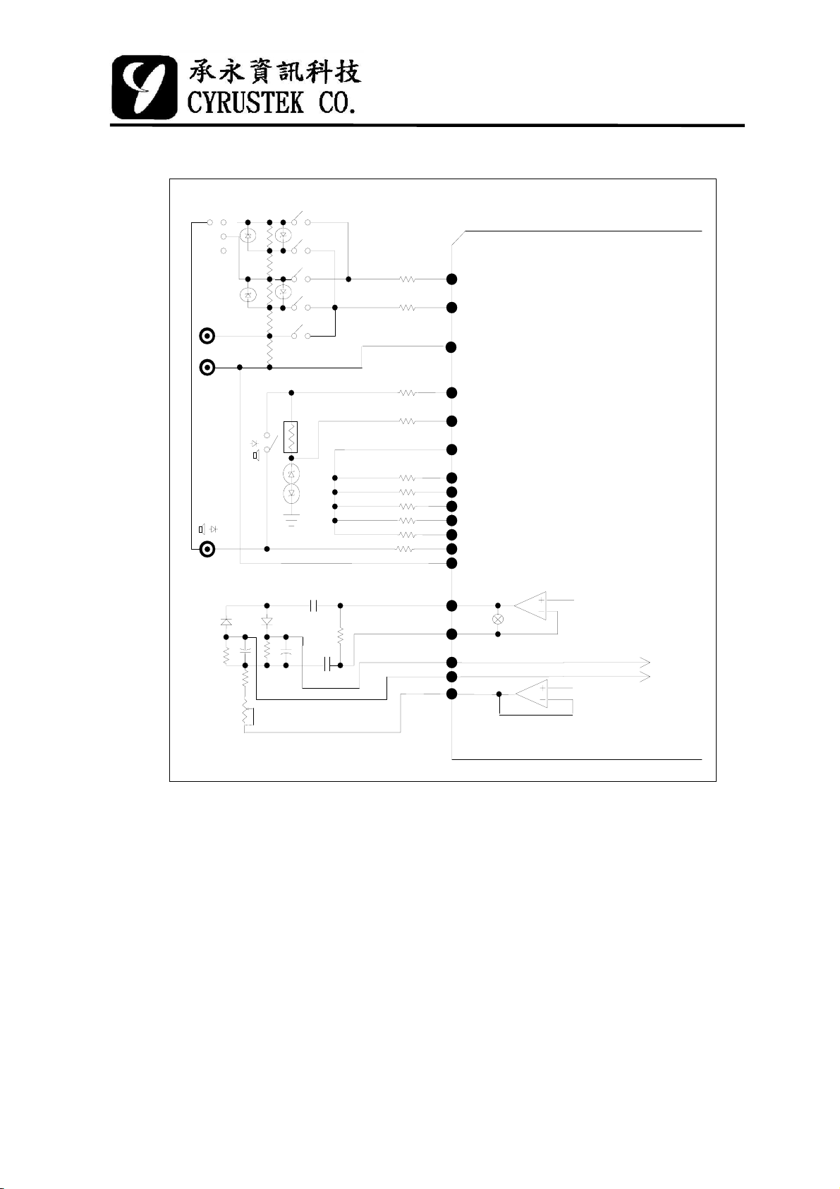
(1) Measurement Description
Voltage Measurement
Resistive divider is automatically changed to provide in range reading
for 399.9mV to 3999V full scale reading. The following table shows
the various full scale range.
Range Full scale Resistive Ratio
VR1
VR2
VR3
VR4
VR5
Resistance Measurement
399.9 mV
3.999 V
39.99 V
399.9 V
3999 V
1 , 1/1
R2/(R1+R2) , 1/10
R3/(R1+R3) , 1/100
R4/(R1+R4) , 1/1000
R5/(R1+R5) , 1/10000
Resistive divider is automatically changed to provide the proper range.
The following table shows the various full scale range.
Range Full Scale Reference Resistor
OR1 399.9 Ω
OR2 3.999 KΩ
OR3 39.99 KΩ
OR4 399.9 KΩ
OR5 3.999 MΩ
OR6 39.99 MΩ
Current Measurement
In the current measurement mode , there are three range selections :
Mode Range Selection Full Scale
Automatic Mode 1 uA 399.9 uA
Automatic Mode 2 mA 39.99 mA
Manual Mode A 39.99 A
When the mode changes among (uA, mA, A), the original AC/DC
state will keep.
R6(100Ω)
R5(1KΩ)
R4(10KΩ)
R1||R3(=100KΩ)
R1||R2(=1MΩ)
R1(10MΩ)
3999 uA
399.9 mA
7 91年11月28日
Page 8

ES519
60
MM
3 3/4 Auto D
Continuity Check
The continuity check is the same as the 399.9Ω range of the resistance
measurement mode (manual mode). If the bargraph number <=3 , there will
2.0 KHz signal comes out from BUZOUT pin, if the bargraph number >=4,
there will be no beep exist.
Diode Measurement
Use the DCV 3.999V range of voltage measurement mode (manual mode ).
If the test circuit is open or the device (diode) under test is larger than 2V,
the LCD display will show "OL", but the bargraph will show the real
detected voltage.
Frequency Counter
The timebase of ES51960 is derived by a clock oscillator.
The timebase of counter is :
T
counter
Thus , the counter will operate with a 1 second timebase when a
4MHz oscillator is used. For accurate frequency measurement,a
crystal oscillator is recommended. The frequency counter can
automatically or manually select the proper range. Autorange
operation extends over six decades from 1 Hz to 399.9MHz.
Range Full Scale
FR1
FR2
FR3
FR4
FR5
FR6
3.999 KHZ
39.99 KHZ
399.9 KHZ
3.999 MHZ
39.99 MHZ
399.9 MHZ
4,000,000
=
F
osc
8 91年11月28日
Page 9
60
MM
10A
10A
AGND
uA
mA
450
45
4.5
0.495
0.005
R
uA
uA
mA
mA
10A
1.5K
PTC
100K
100K
100K
100
IVSL
IVSH
AGND
OVX
OVH
OVSG
ES519
3 3/4 Auto D
14
13
100
15
16
17
V.A.R
D1 D2
2.2u
15K
10K
5K
15K
2.2u
Z1
6V
Z2
0.22u
0.1u
R6
100
R5
R4
10K
R3
101K
R2
1.11M
10M
R1
66M
Analog Switch Selection
1K
OR1
VR5
VR4
VR3
VR2
VR1
SGND
ADO
ADI
ACVH
ACVL
TEST5
Note : Light shielding for Z1, Z2, D1, D2.
18
19
20
21
22
32
31
27
26
25
24
23
ES51960
OVSG
INH
INL
9 91年11月28日
Page 10
ES519
60
MM
3 3/4 Auto D
(2) Switch Description
Rotary mode : FC1,FC2,FC3,FC4,FC5
Measurement mode depends on the logic levels of FC1,FC2,FC3,FC4
FC5 and KEY :
When FC5=1
FC1 FC2 FC3 FC4 Mode Push mode(KEY)
1100DC V DC V — AC V
1110DC uA DC uA — AC uA
1101DC mA DC mA — AC mA
1111DC A DC A — AC A
0111
0110Continuity Continuity — Diode
1011
1010Frequency
When FC5=0, KEY is disabled.
ΩΩ— Continuity
ΩΩ— Continuity — Diode
FC1 FC2 FC3 FC4 Mode
1100ACV
1110AC uA
1101AC mA
1111ACA
0111
0110Continuity
1011Diode
1010Frequency
Under ADP mode
(1) FC5=1, when the input value is overflow, the buzzer will beep.
(2) FC5=0, when the input value is overflow, the buzzer will not beep.
FC1 FC2 FC3 FC4 Mode
0101ADP0
1001ADP1
0011ADP2
0001ADP3
0100ADP0(no bar)
1000ADP1(no bar)
0010ADP2(no bar)
0000ADP3(no bar)
Ω
10 91年11月28日
Page 11
60
MM
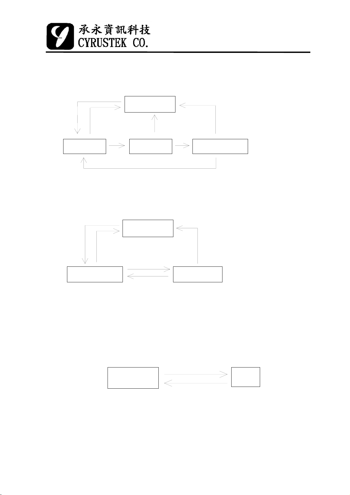
Push mode
MAX/MIN :
1 push < 1 sec
RESET
(AUTOMATIC)
ES519
3 3/4 Auto D
1 push > 1 sec
"MAX" active
max value
1 push > 1 sec
"Min" active
min value
1 push <1 sec
1 push > 1 sec
"MAX MIN" blink
current value
(1) If MAX/MIN function is enaled, REL function is disabled, or if
REL function is enabled,MAX/MIN function is disabled.
(2) The sequence order is MAX value, MIN value, Current value.
REL :
RESET
(AUTOMATIC)
1 push >1 sec1 push <1 sec
"REL" active
the relative value
1 push<1 sec
"REL" blink
the Di(N) value
1 push >1 sec
* When REL function is enabled :
Display = Di(N+K) - Di(N) , K = 0,1,2,3, ...
Di(N) : Input reading when REL function active.
Di(N+K) : Next K step input reading.
* If the input value Di(N) or Di(N+K) ≧ (± 4000), the relative value will
display “OL”.
HOLD :
1 push
RESET
(Automatic)
Data
Hold
(1) Under auto mode, press the HOLD function, the mode will change to
manual mode and stay at the same scale range.
(2) If HOLD function is enabled, MAX/MIN, REL function is disabled.
but if MAX/MIN, REL function is pressed first, the HOLD function
still can active.
11 91年11月28日
Page 12
ES519
60
MM
p
3 3/4 Auto D
(3) If continue to press the HOLD pin(logic low)then power on the
ES51960, all the segments will blight until release the HOLD pin.
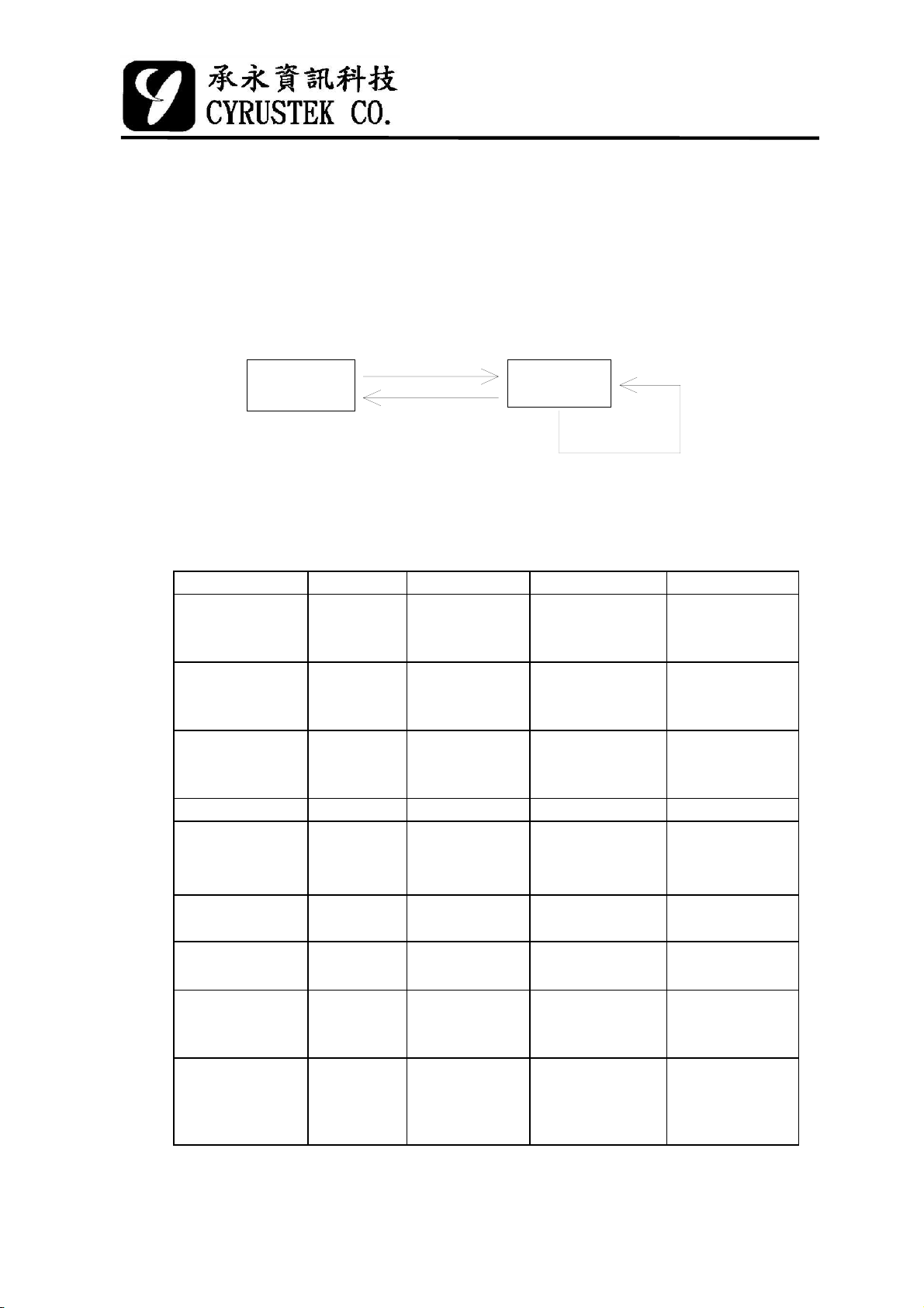
Range :
The mode selection of Auto-mode and Manual-mode is determined
by RANGE pin. The following is the operating flow chart of Auto-mode
and Manual-mode.
1 push < 1 sec
Automatic
Mode
1 push > 1 sec
* If HOLD, MAX/MIN, REL function is enabled,when RANGE
function is pressed,the enabled function will be clear.
* The bargraph is not affected by HOLD, MAX/MIN, REL function.
Manual
Mode
1
ush < 1 sec
Range up
Function Auto Manual Control Range Initial Range
Voltage
(AC/DC)
uA(AC/DC)
mA(AC/DC)
A(AC/DC) Fix Fix 39.99A 39.99A
Ω R1-R6 Ri → Ri+1
Continuity Fix Fix
Diode Fix Fix 3.999V "OL"
Frequency
ADP0
ADP1
ADP2
ADP3
R1-R5 Ri → Ri+1
(R5→R1)
R1-R2 R1 → R2
R2 → R1
R1-R2 R1 → R2
R2 → R1
(R6→R1)
FR1-FR6 FRi→FRi+1
(FR6→FR1)
Fix Fix NOTE XXXX
399.9mV
|
3999V
399.9uA
|
3999uA
39.99mA
|
399.9mA
399.9Ω
|
39.99MΩ
399.9Ω
3.999KHZ
|
399.9MHZ
399.9mV(DC)
3.999V (AC)
399.9uA
39.99mA
"OL"
399.9Ω
"OL"
399.9Ω
3.999V
3.999KHZ
XXX.X
XX.XX
X.XXX
12 91年11月28日
Page 13
ES519
60
MM
3 3/4 Auto D
Auto-Power-off function
Once power on the ES51960, the auto-power-off function will be enabled
and if the functions are not changed in 30 minutes, the auto-power-off condition
will happen and SLEEP pin output will change from +3V to –3V. When poweroff happens, the final data is saved. If continue to press anyone of the pushed function
(except HOLD pin)then power on the ES51960, the auto-power -off function will be
disabled , and LCD segment "APO" will be turned off.
BKLIT
When this pin BKLIT is pushed, the BKOUT pin output will change from
V- to V+ for 60 sec then returned to V- again, but if this pin is pushed again
within 60 sec, this function will be canceled.
SLEEP
When auto-power-off happens, this pin output will change from V+ to V-, once
re-power on happen, this pin output will change from V- to V+.
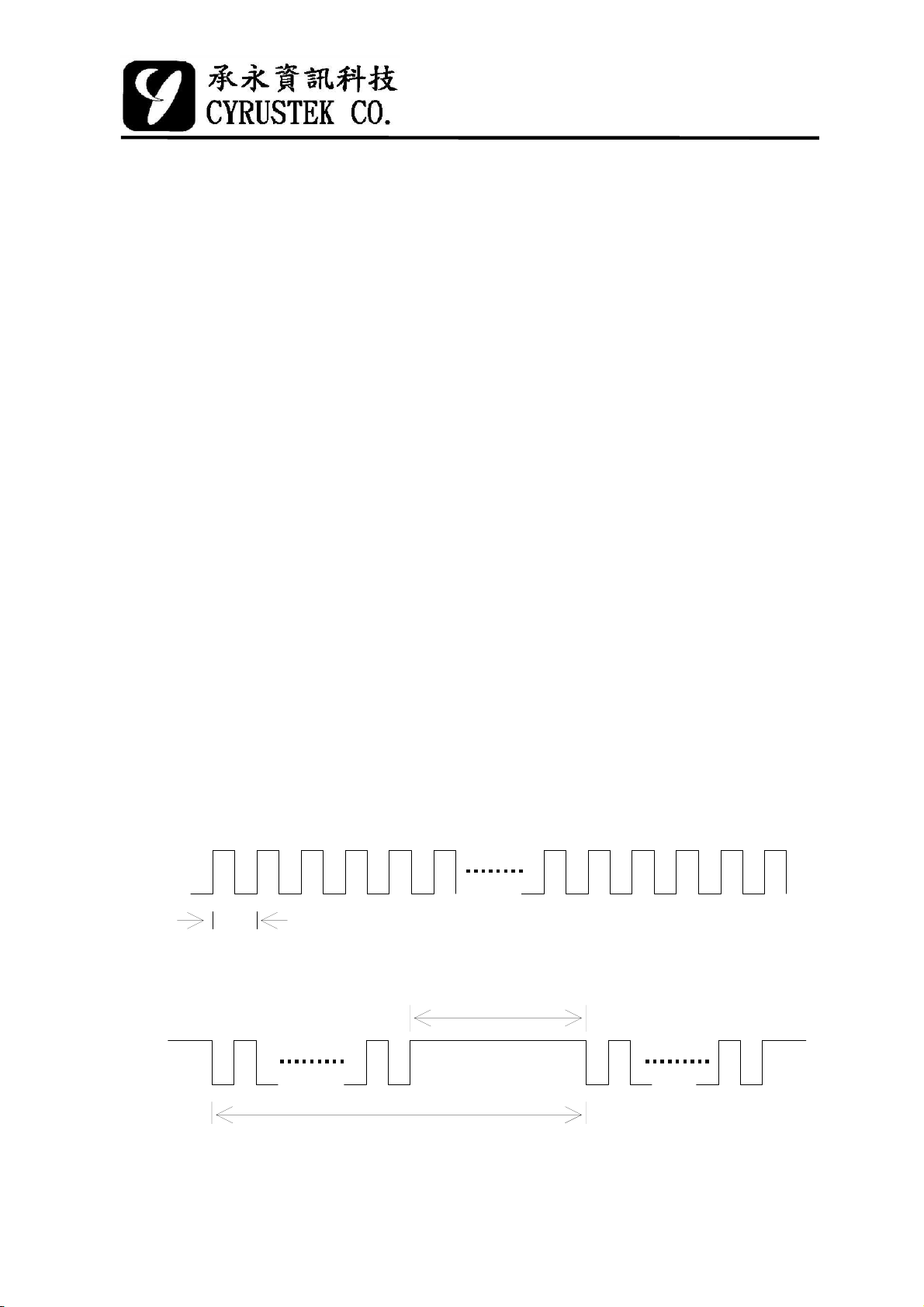
(3) Buzzer
The BUZZER turns on in the following condition :
•1 beep : Measurement function changed ,power and re-power on ,
RANGE, HOLD, MAX/MIN, REL, SET, BKLIT or KEY are pushed.
• 3.3 beeps : Input reading overrange. (except diode, ohm, continuity,
frequency function used)
• 2.0 KHZ continue: Continue check (Bargraph number<=3).
• 2.0 KHZ continue 1.5 sec : Auto-power-off.
BUZZER output waveform :
2.0 KHz ( continued )
beeps (3.33 beeps/sec)
0.5 mS
0.15 sec
0.3 sec
13 91年11月28日
Page 14
ES519
60
MM
3 3/4 Auto D
(4) Serial Data Output
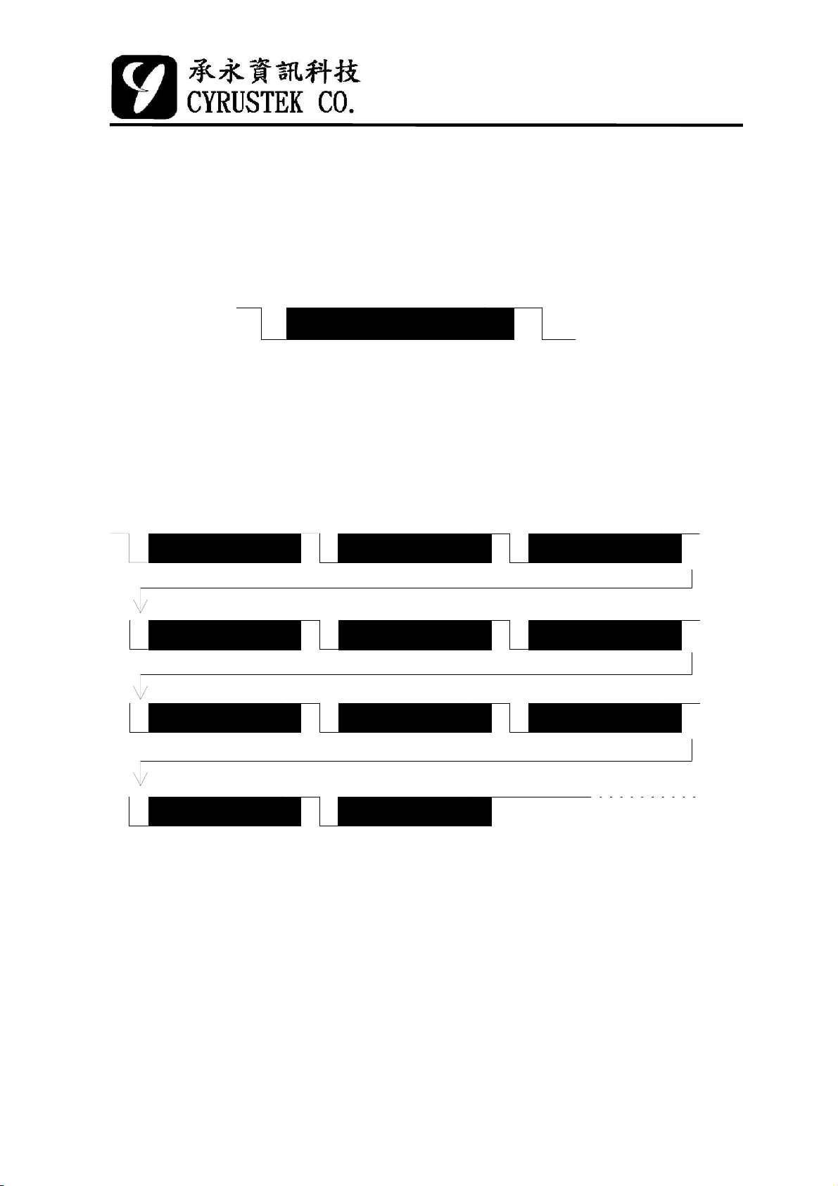
The serial data is output two times from SDO pin on each A/D conversion cycle.The
data format satisfy JIS 7BIT transmission code and the baud rate is 2400,it means the
receiver terminal can use RS-232 interface to read data .
single package
0V
-3V
0
D0 ~D6
p
1P
LSB MSB
A single package include a start bit(0),D0~D6(7 bit), a parity check bit(odd) and a
stop bit(1). All the data stream is consist of 110× 2 bits. The high and low voltage levels
correspond to DGND and V- respectively. SDO remains at 1 (high) when it is inactive.
Hence the start bit (0) could be used as triggering signal to begin the reading process.
all package
0
range
0
0
p
1
0
p
1 0
digit0digit1
p
1 0
p
1 0
digit2digit3
p
1 0
function
p
1 0
p
1
p
1
p
1
status
0
CR LF
Digit0 ~ 3 data is exactly the receiver display number,but the status, function,range,
option1,option2 data all need written program to judge what the data mean.
Note : LSB bit is sent first,then MSB bit.
The meter always outputs the current input value to the serial port in spite of HOLD
mode. Each block is repeated twice in one conversion cycle. The detailed data format of
each packet is listed below.
14 91年11月28日
p
1 0
option1
p
1
option2
Page 15
ES519
60
MM
3 3/4 Auto D
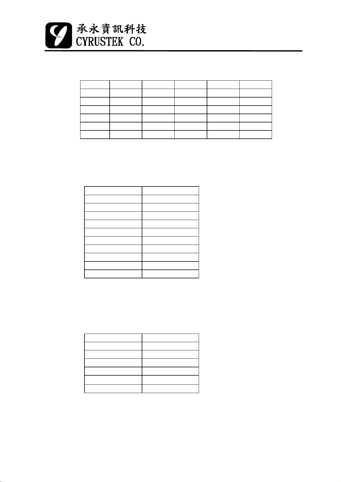
RANGE :
Range V mA uA Ohm Frequency
0110000 400mV 40mA 400uA 400 Ohm 4K HZ
0110001 4V 400mA 4000uA 4K Ohm 40K HZ
0110010 40V 40K Ohm 400K HZ
0110011 400V 400K Ohm 4M HZ
0110100 4000V 4M Ohm 40M HZ
0110101 40M Ohm 400M HZ
Because Continuity,Diode, Current(A) and ADP measurement range
are all fixed,so they are all the first code 0110000.
DIGIT0 ~ 3 :
Digit Display data
0110000 0
0110001 1
0110010 2
0110011 3
0110100 4
0110101 5
0110110 6
0110111 7
0111000 8
0111001 9
If the input value is over-range(OL),the reading data DIGIT3=4,DIGIT2=0,
DIGIT1=0,DIGIT0=0,but under the frequency mode,DIGIT0~3 output the
measured value.
FUNCTION : The definition code is not the same as FC1 ~ FC5.
Function Measurement mode
0111111 A
0111110 UA
0111101 MA
0111100 Voltage
0110111
0110110 Continuity
Ω
15 91年11月28日
Page 16
ES519
60
MM
3 3/4 Auto D
0111011 Diode
0111010 Frequency
0110101 ADP0
0111001 ADP1
0110011 ADP2
0110001 ADP3
0110100 ADP0*
0111000 ADP1*
0110010 ADP2*
0110000 ADP3*
*Under ADP* mode, the bargraph will not display
STATUS :
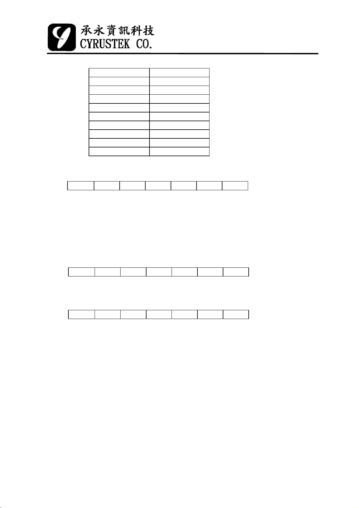
0 1 1 - BATT ACOL OL
BIT7 BIT6 BIT5 BIT4 BIT3 BIT2 BIT1
- : "1" is for the negative(-).
BATT : "1" is for the battery voltage is less than 2.3V± 0.2V.
OL : "1" is for the input voltage over-range.
ACOL : "1" is that the offset value of input signal is too large on the AC mode.
OPTION1 :
0110000
BIT7 BIT6 BIT5 BIT4 BIT3 BIT2 BIT1
OPTION2 :
0 1 1 DC/AC AUTO MAN APO
BIT7 BIT6 BIT5 BIT4 BIT3 BIT2 BIT1
DC/AC : "1" is for the DC mode and Ω, Diode, Continuity, ADP, Frequency
Function, "0" is for the AC mode.
AUTO : "1" is for auto range.
MAN : "1" is for the manual range.
APO : "1" is for the auto-power-off function enabled.
CR(BACK) : Transmission code "0001101".
LF(LINE FEED) : Transmission code "0001010".
16 91年11月28日
Page 17
60
MM
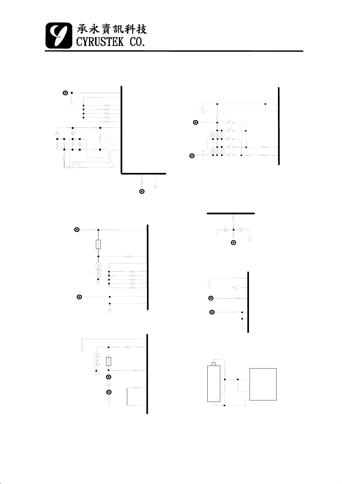
TEST CIRCUIT
T
R
ES519
3 3/4 Auto D
1 Voltage
D2
D1
15K
15K
10K
5K
2 Resistor
3 Diode
4 Current
AGND
100
1K
10K
101K
1.11M
0.47u
PTC
1.5K
Z1
6V
Z2
88M
0.1u
1.0u1.0u
OVSG
OR1
VR5
VR4
VR3
VR2
ADO
ADI
ACVH
ACVL
TEST5
100
1K
10K
101K
1.11M
Voltage
100
V
R
1
10M
V
R
-100mV
OVX
OVH
OVSG
OR1
VR5
VR4
VR3
VR2
SGND
AGND
mA
0.005
0.495
4.5
uA
45
450
10A
5 Frequency
V-
6 ADP
-100mV
ADP
200
2.2u
PTC
10A
mA
mA
uA
uA
F
R
E
Q
Fin
100K
1.5K
VA+
VA-
ADP
SGND
AGND
100K
100K
AGND
SGND
IVSH
IVSL
100
Z1
6V
Z2
17 91年11月28日
PTC
1.5K
10M
1.11M
AGND
OVH
VR1
VR2
OVSG
7 Low battery
9V
680K
BA
TE
Y
270K
0V
ES51960
LBAT9
0.1u
AGND
V-
Page 18
60
MM
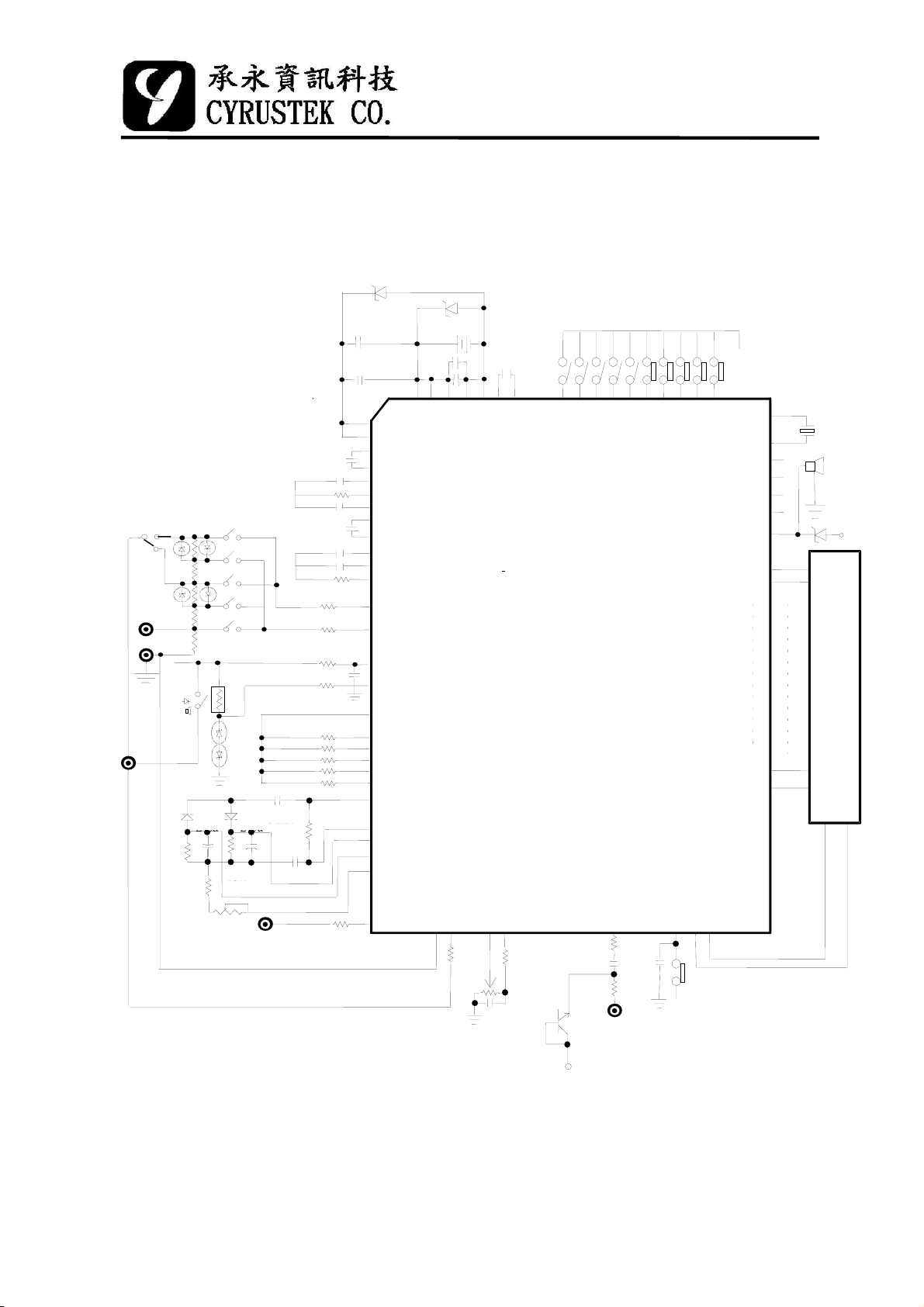
APPLICATION CIRCUIT
7.5V ZI
0.1u
+
10u
V+
V+
0.1u
CH+
CHCIH
BUFH
CAZH
CL+
CL-
CIL
CAZL
BUFL
IV S L
IV S H
OVX
OVH
OVSG
OR1
VR5
VR4
VR3
VR2
ADO
ADI
ACVH
ACVL
TEST5
VA+
VA-
ADP
uA
mA
4.5
10A
AGND
45
D1
22K
15K
R
10K
450
1u
0.495
0.005
D2
5K
1.5K
PTC
Z1
6V
22K
15K
uA
uA
mA
mA
10A
2.2u2.2u
0.22u
1u
ADP
101K
1.11M
0.47u
0.1u
0.022u
200K
0.047u
0.22u
0.47u
200K
100
1K
10K
0.01u
0.1u
100K
100K
100K
100
66M
88M
100K
A
G
N
D
10u
0.1u
A
G
N
D
S
G
N
D
3V
+
D
G
N
D
V
R
1
10M
5.6V ZI
V
V
-
-
A
D
O
V
D
R
C
10k
+
ES519
3 3/4 Auto D
0.1u
M
R
H
A
E
O
X
L
L
/
D
M
I
N
S
E
G
S
2
E
4
T
-3 V
1u
S
C+C
D
O
A
C
V
V
R
H
R
91k
C1815
NPN
F
F
L
C
C
B
2
1
A
T
9
B
S
K
L
L
E
I
E
T
P
200
2.2u
PTC
F
F
C
3
F
R
E
Q
F
C
4
C
5
4.7n
1.5K
R
A
N
G
E
-3 V
B
K
OSC2
K
E
O
Y
OSC1
U
PH 4
T
PH 3
PH 2
PH 1
BUZOUT
BUZIN
BP1
BP2
S
E
G
2
3
4 M HZ
-3 V
L
C
D
D
I
S
P
L
A
Y
-3 V
18 91年11月28日
Page 19
ES519
60
MM
3 3/4 Auto D
The Other
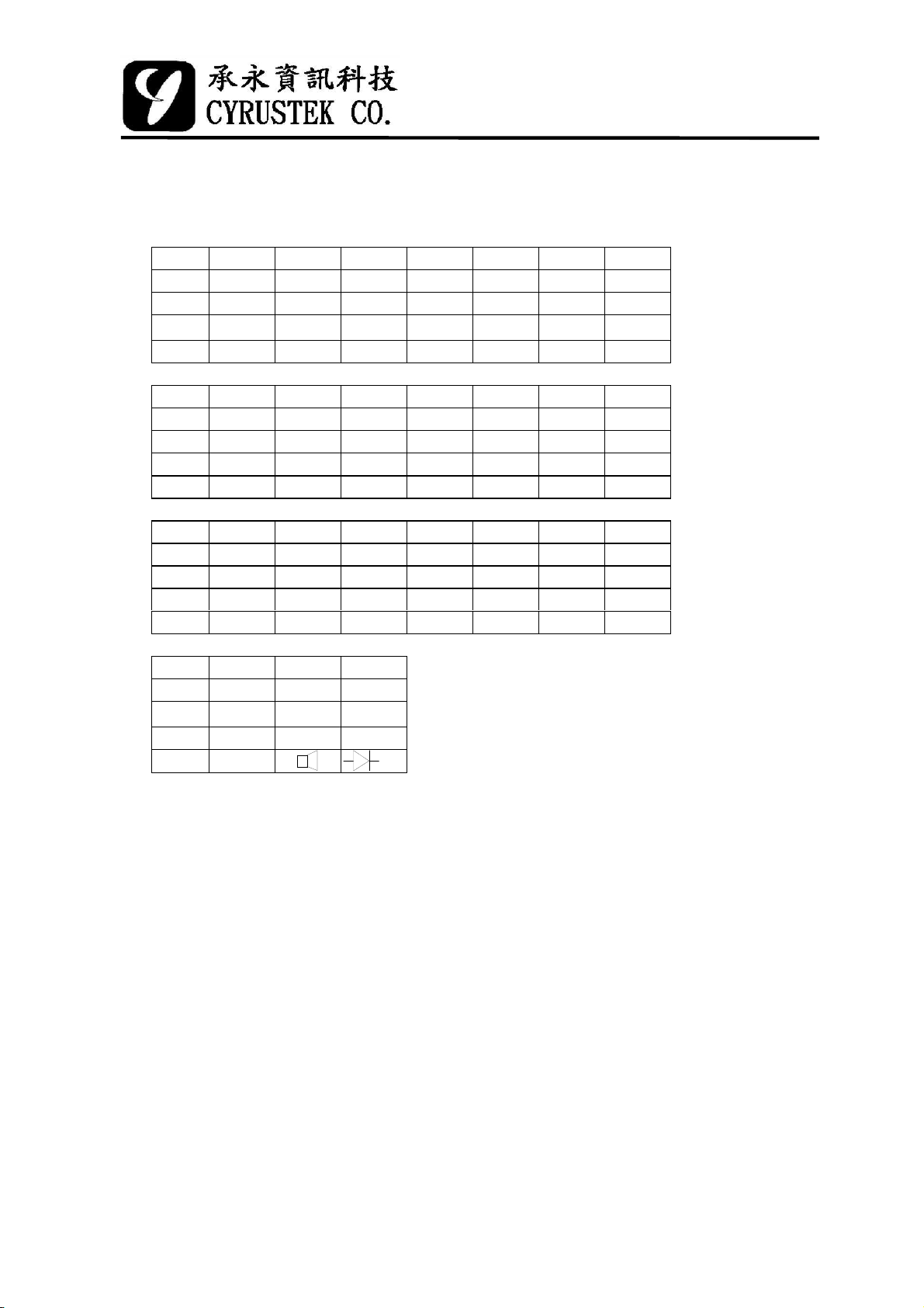
(1) LCD pin assignment
SEG1 SEG2 SEG3 SEG4 SEG5 SEG6 SEG7
BP1 RS232 bar2 bar4 bar6 bar8 bar9 bar11
BP2 Bar0 bar1 bar3 bar5 bar7 d3 bar10
BP3 Bar-
BP4 DC BATT f3 AC AP0 a3 b3
SEG8 SEG9 SEG10 SEG11 SEG12 SEG13 SEG14
BP1 bar13 bar15 bar16 bar18 bar20 bar22 bar24
BP2 bar12 bar14 d2 bar17 bar19 bar21 bar23
BP3p3e2g2c2pxp2e1
BP4 REL f2 a2 b2 HOLD MAX f1
-
AUTO MANU e3 g3 c3
SEG15 SEG16 SEG17 SEG18 SEG19 SEG20 SEG21
BP1 bar25 bar27 bar29 bar31 bar32 bar34 bar36
BP2 d1 bar26 bar28 bar30 d0 bar33 bar35
BP3g1c1p1e0g0c0M
BP4 a1 b1 MIN f0 a0 b0 u
SEG22 SEG23 SEG24
BP1 bar38 bar40 HZ
BP2 bar37 bar39
BP3 K V A
BP4 m
NOTE : 1 : "bar0" is normally ON.
2 : "p1" is always ON when ADP1 function is used.
3 : "p2" is always ON when ADP2 function is used.
4 : "p3" is always ON when ADP3 function is used.
5 : "px" is always OFF(not used).
6 : "RS232" is always ON when SDO function is enabled(option).
Ω
19 91年11月28日
Page 20
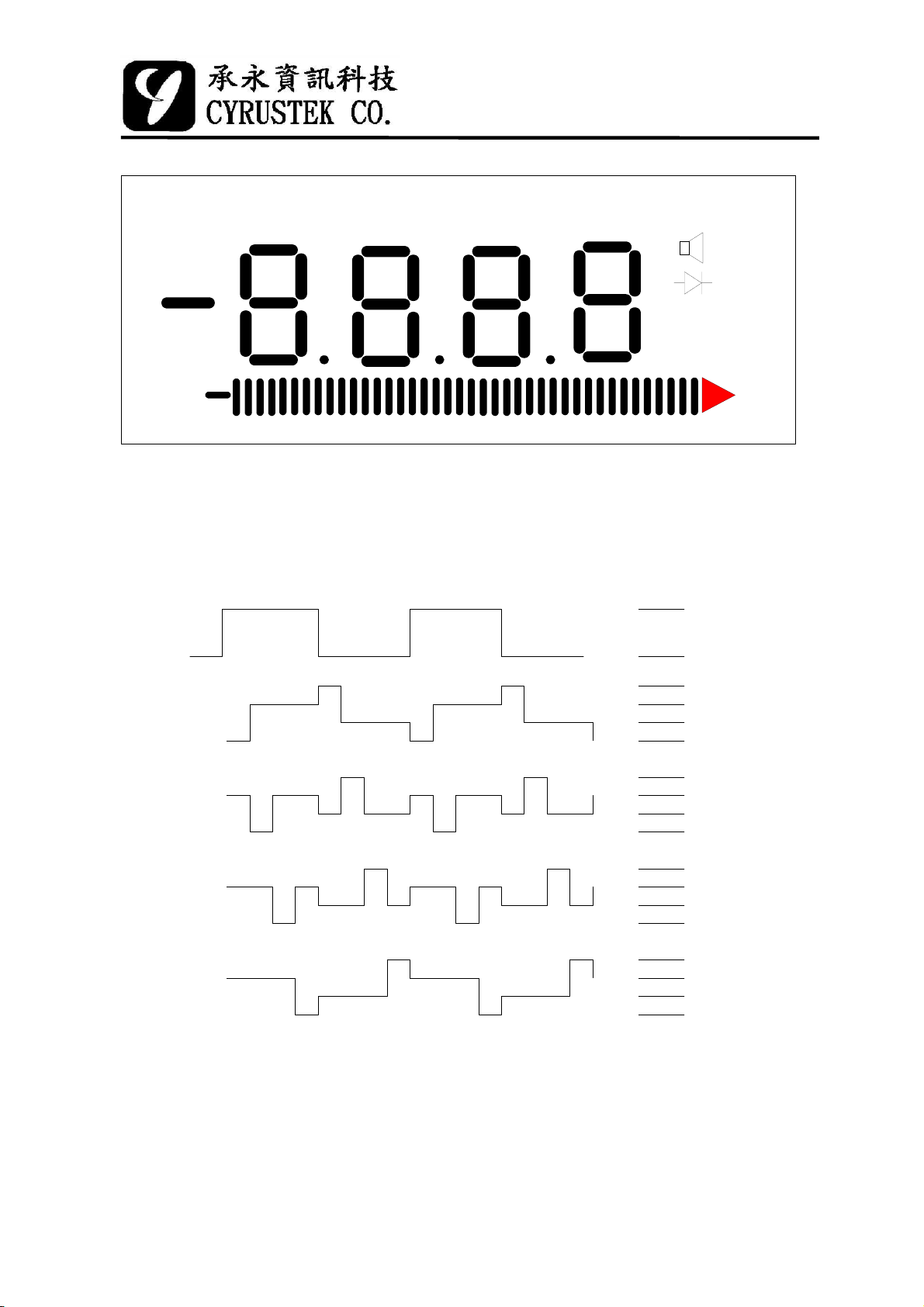
ES519
60
MM
BATT APO REL HOLD MAX MIN
RS232
DC AC
AUTO
MANU
LCD Display Panel
3 3/4 Auto D
umVA
Ω
MK
HZ
Backplane Waveform (Frequency = 62.5 HZ)
ANNUNC
BP1
BP2
BP3
(V-)+3V
V-
(V-)+3V
V-
(V-)+3V
V-
(V-)+3V
V-
(V-)+3V
BP4
V-
20 91年11月28日
Page 21

ES519
60
MM
3 3/4 Auto D
(2) LCD Display ON Condition
LCD Annunciator
"BATT" Low battery is detected.
"DC" DC voltage and DC current functions are
used.
"AC" AC voltage and AC current functions are
used.
"-" DC voltage and current function.
"AUTO" Automatic mode is used.
"MANU" Manual mode is used.
"REL" REL function is used.
"HOLD" HOLD function is used.
"MAX" MAX function is used.
"MIN" MIN function is used.
" "&"Ω"
" "&"V"
"mV" AC/DC voltage function is used.
"umA" AC/DC current function is used.
"MKΩ" Ω measurement function is used.
"MKHZ" Frequency counter is used.
"APO" Auto-power-off function is used.
"RS232" Serial data output is used.
Bargraph Bargraph annunciator is only depend on input
Continuity-check is used.
Diode measurement is used.
reading .
21 91年11月28日
Page 22
ES519
60
MM
3 3/4 Auto D
(3) DC offset value at the ACV
Generally when we measure an ac voltage,it may be biased upon a dc level.Once the
offset voltage is too large,the measurement data will not be true.There is one method can
remind user to notice this condition.Connecting ADODC (pin 33) to -3V,when the above
condition happens,the LCD symbol "dc" will blink and the data display will be "OL",then
user can press RANGE pin to enter to the next range and get the correct value.If this
function is enabled ,user also can read this condition from the RS232 output form(status).
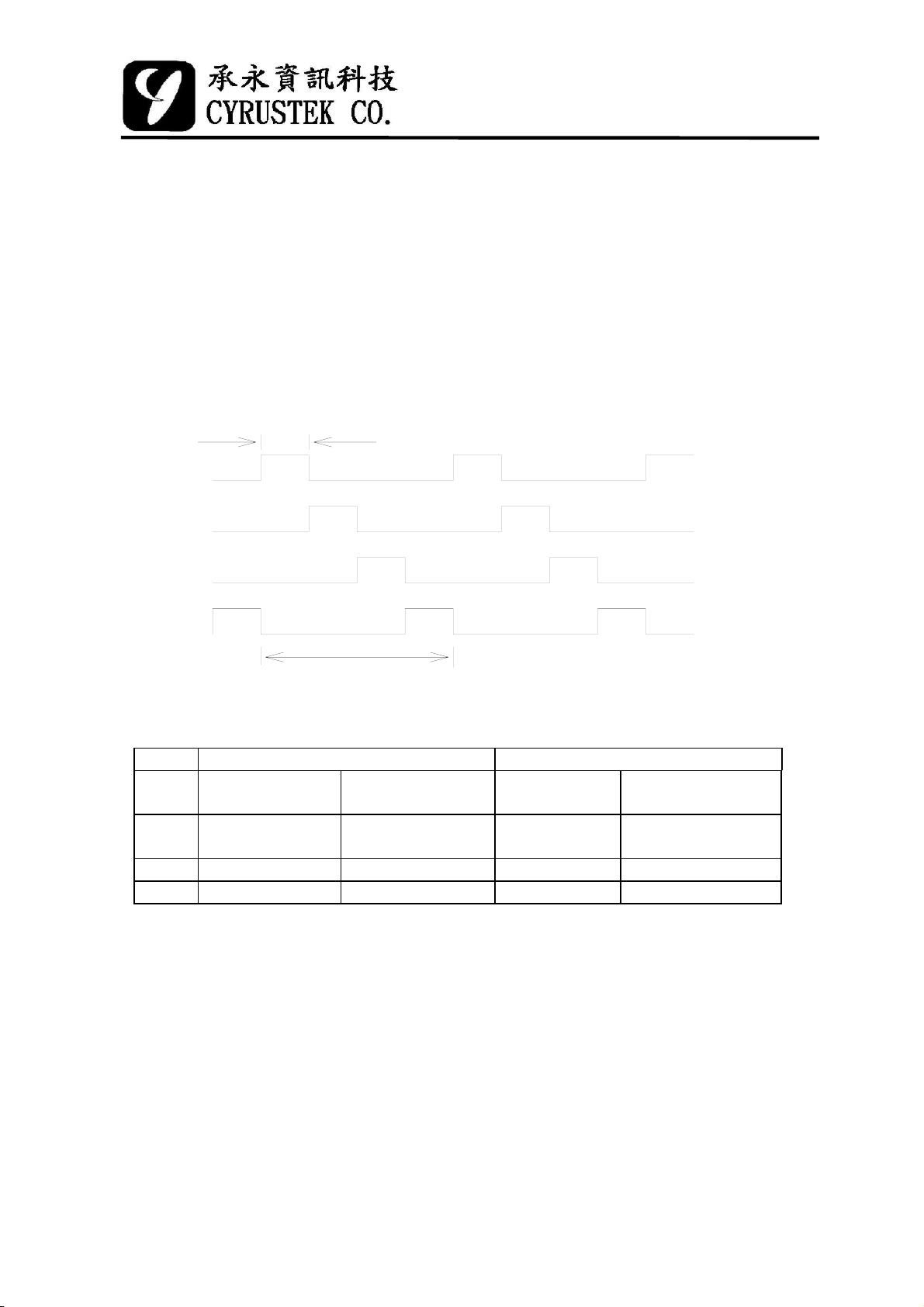
(4) PH1,PH2,PH3,PH4 four phase output
PH1
32ms
PH2
PH3
PH4
128ms
(5) High Resolution and High Speed(Bargraph) time
High Resolution High Speed
Mode Current(I)
Measurement
ZI
AZ
INT 100m sec 100m sec 10m sec 10m sec
DEINT 200m sec 400m sec 20m sec 40m sec
100m sec
150m sec
Other Measurement
(V,R)
100m sec
150m sec
Current(I)
Measurement
10m sec
15m sec
Other Measurement
(V,R)
10m sec
15m sec
22 91年11月28日
Page 23
60
MM
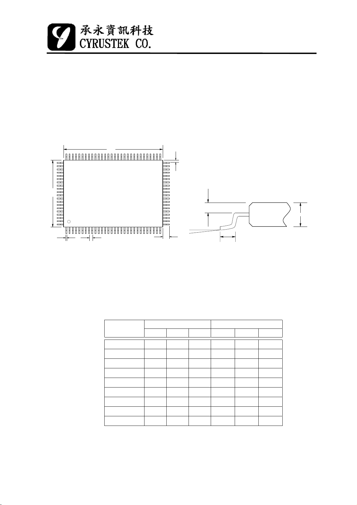
Package
1 100 Pin QFP Package
W
L
ES519
3 3/4 Auto D
A
2 Dimension Paramenters
BC
Symbol
W 19.90 20.00 20.10 783.5 787.4 791.3
L 13.90 14.00 14.10 547.2 551.2 551.2
A 0.425 16.7
B 0.20 0.30 0.40 7.9 11.8 11.8
C 0.65 25.6
d 1.05 1.20 1.35 41.3 47.2 47.2
a 2.57 2.72 2.87 101.2 107.1 107.1
D 2.50 98.4
θ
b
θ
D
Milimeter Mill
Min. Typ. Max. Min. Typ. Max.
o
0
10
o
d
a
23 91年11月28日
 Loading...