

Page 1

ESS Technology, Inc. SAM0367-022101 1
ESS Technology, Inc.
ES1980 Maestro-3
PCI Audio-Modem Accelerator
Product Brief
DESCRIPTION
The ES1980 Maestro-3 PCI audio-modem accelerator
combines advanced audio and modem functionality in a highly
integrated PCI solution for notebook systems. It uses the highbandwidth PCI bus to deliver advanced PC audio features, such
as HRTF 3D positional audio, DirectSound acceleration and
DVD AC-3 5.1 to 2 speaker virtualization.
The ES1980 implements multistream DirectSound and
DirectSound3D acceleration with digital mixing, sample rate
conversion, and HRTF 3D filtering. The ES1980 maintains full
DOS legacy audio compatibility over the standard PCI 2.1 and
PCI 2.2 buses. The ES1980 is designed for high-performance
consumer multimedia notebook PC applications.
The ES1980 includes a programmable audio signal processor
and provides simultaneous support for multiple audio streams.
With its built-in DSP core, the ES1980 uses its dedicated direct
memory access (DMA) engine to handle complex signal
processing tasks with a bus-mastering PCI interface.
The support functions ensure efficient transfer of audio data
streams to and from system memory buffers, providing a system
solution with maximum performance and minimal host CPU
loading. The architecture enables implementation of
communications over the Internet from multiple sources.
The ES1980 incorporates an HSP modem interface via its ACLink connecting with the ES2828 MC‘97 codec. The MC‘97 is
used as the analog front end for the modem and DAA control.
The V.90 modem runs on the host while the ES1980 serves as
the bidirectional buffer for data transmission and reception. The
modem functions include the standard AT command set, V.42bis
and Group 3 fax.
The ES1980, which operates at 3.3V digitally, is compliant with
the Advanced Power Management (APM) 1.2, Advanced
Configuration and Power Interface (ACPI) 1.1, and PCI Power
Management Interface (PPMI) 1.1. The ES1980 supports D0,
D1, D2, and D3 power-saving modes for power efficiency when
the audio system is both active and idle.
The ES1980 provides a high-quality docking solution and
supports an AC-link based digital docking solution with its
secondary AC‘97 Extension 2.1 compliant interface. CLKRUN#
pin support can be used to stop the PCI interface clock. This
helps achieve the lowest power consumption in D3
hot
state.
The ES1980 provides full DOS game compatibility through three
hardware implementations: PC/PCI, distributed DMA (DDMA),
and transparent DMA (TDMA).
The ES1980 is available in an industry-standard 100-pin lowprofile quad flat pack (LQFP) package.
AUDIO FEATURES
• High-performance PCI audio acceleration
• Multistream DirectSound and DirectSound 3D acceleration
• Sensaura CRL positional 3D
• High-quality sample rate conversion and digital mixing
• AC-3 speaker virtualization
• Direct music support
• Realtime effects processing
• Digital docking with secondary AC-Link
• S/PDIF output for DVD content
• EEPROM interface for SID and SVID
• Full legacy DOS game support using PC/PCI, DDMA, or TDMA
hardware implementation methods
• Supports up to two additional PCI bus master devices
• V.90 HSP modem interface via MC‘97 link
POWER MANAGEMENT
• Compliance with APM 1.2, ACPI 1.1, and PPMI 1.1
• Compliance with Intel’s Mobile Power Guidelines ‘99
• 3.3V digital operation with 5V-tolerant inputs
COMPATIBILITY
• Supports PC games and applications for SoundBlaster and
SoundBlaster Pro
• Meets PC99/PC2001 and WHQL specifications
• Compliant with Intel’s audio-modem riser card and mini-PCI
specifications
MODEM FEATURES
• Data mode capabilities:
—– V.90 56 kbps
—– V.34 33.6 kbps and fallbacks
—– Standard AT command set
—– V.42 (LAPM) and MNP4 error correction
—– V.42bis/MNP 5 data compression
• Fax Mode capabilities:
—– ITU-T V.17, V.21 ch2, V.27ter, V.29
—– Group 3 (TIA/EIA 578 Class 1 and Class 2)
• Supports wake-on-ring from D3
hot
and D3
cold
state
Page 2
2 SAM0367-022101 ESS Technology, Inc.
ES1980 PRODUCT BRIEF
PINOUT
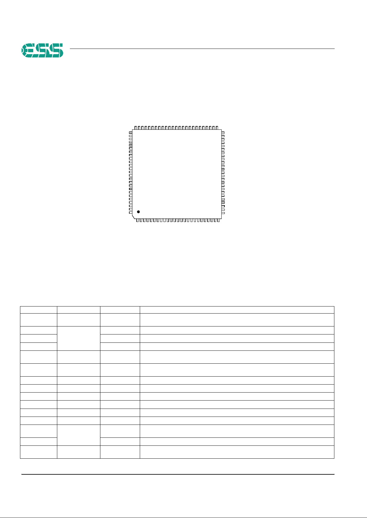
Figure 1shows the ES1980 pinout diagram.
Figure 1 ES1980 Maestro-3 Pinout Diagram
ES1980 PIN DESCRIPTIONS
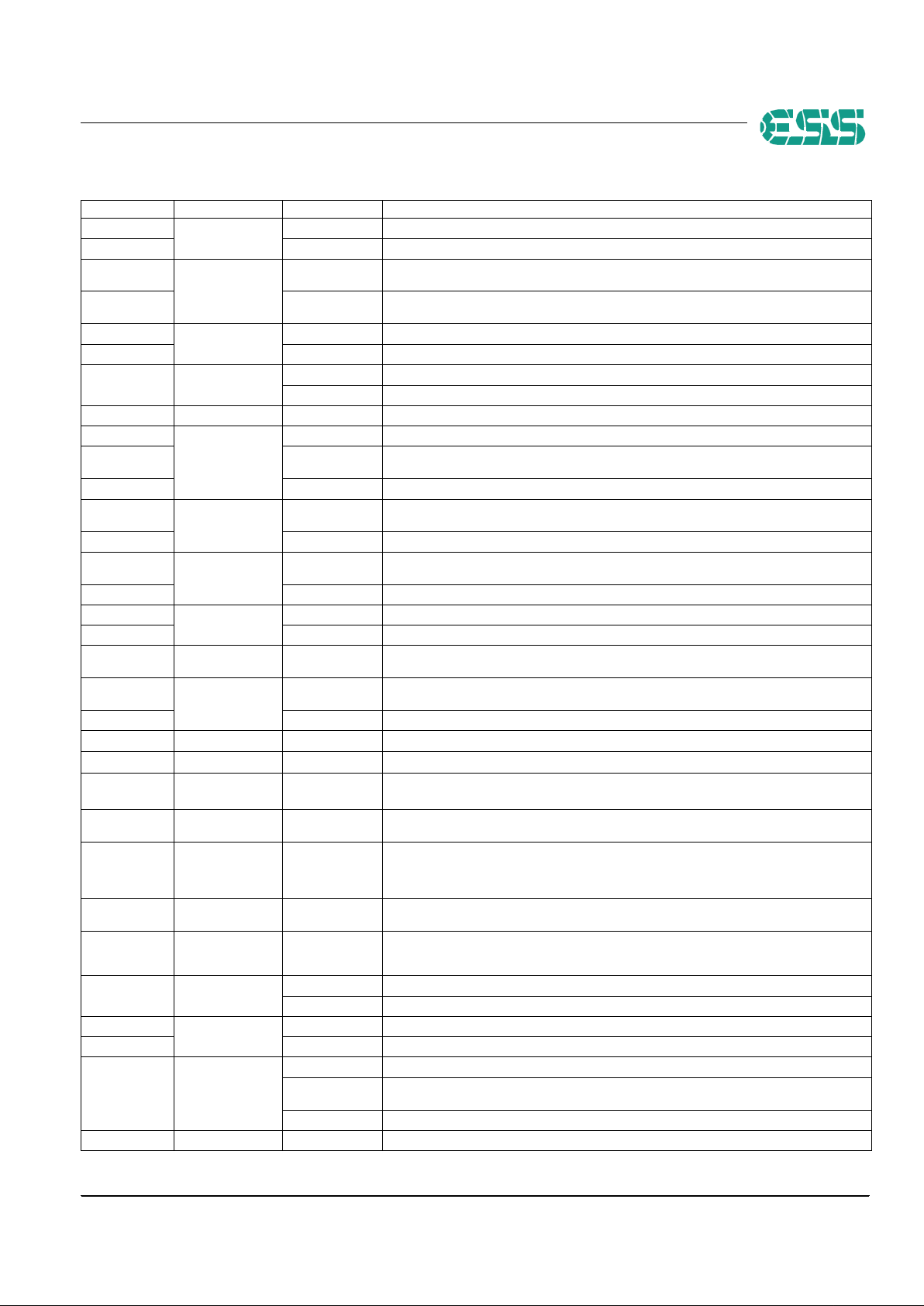
Table 1 lists the ES1980 pin descriptions.
1
GPIO5/VOLUP#
GPIO4/VOLDN#
GPIO14/R1#
GPIO10/GS1/GT1#
GPIO7
GPI08/I
2
SDATA
GPIO12/I
2
SLR
CLKRUN#/ECS
GPIO6/I
2
SCLK
AD1
AD0
AD2
AD3
AD4
AD5
AD6
AD7
VDD
CBE0#
TXD
RST#
INT#
VDD
PCICLK
GNT#
GND
REQ#
GND
AD31
AD30
AD29
AD28
AD27
AD26
AD25
AD24
VDD
SDI2
GPIO 3/ SRST2 #
GPIO 11/ SI RQ/SPDI F O
GND
OSCI
OSCO
VD D
GD0
GD1/ EDOUT
GD2/ VOLUP #/EDI N
GD3/ VOLDN #/E CL K
GD4
GD5
GD6
GD7
GND
SCLK1
SDFS1
GPIO1/GS0/GT0#
SDO1
SDI1
RI NG #/MC9 7DI
PME#
VAUX
VAUXDET
SDFS2
SDO2
SCLK 2
GPIO 0/ SRST1 #
ES1980S
25
GPIO 2/R0#
STOP#
DE VS EL #
TRDY#
IR DY#
FRAME#
CBE2 #
VDD
AD16
AD17
AD18
AD19
AD20
AD21
AD22
AD23
GND
IDSE L/ GPI O9 /PCGN T#
CBE3 #
AD8
AD9
AD10
AD11
AD12
AD13
AD14
AD15
GND
PA R
2 3 4 5 6 7 8 9 10 11 12 13 14 15 16 17 18 19 20 21 22 23 24
75 5174 73 72 71 70 69 68 67 66 65 64 63 62 61 60 59 58 57 56 55 54 53 52
100
76
99
98
97
96
95
94
93
92
91
90
89
88
87
86
85
84
83
82
81
80
79
78
77
26
50
27
28
29
30
31
32
33
34
35
36
37
38
39
40
41
42
43
44
45
46
47
48
49
Maestro-3
CBE1#
RXD
GND
GPIO13/PCREQ#
C24/GPIO15/SPDIFO
100-Pin LQFP
Table 1 ES1980 Pin Descriptions
Name Pin Numbers I/O Descriptions
C/BE[3:0]# 1, 13, 21, 31 I/O PCI command/byte enable pins. During address phase of a transaction, these pins define the bus
command. During data phase, these pins define the byte enable.
IDSE
2
I ID select.
GPIO9 I/O General-purpose input/output; internally pulled up to VDD.
PCGNT# O PC/PCI grant input.
GND 3, 22, 41, 63, 75,
88, 91
I Digital ground.
AD[31:0] 4:11, 23:30, 33:40,
92:99
I/O Address and data lines from the PCI bus.
VDD 12, 32, 66, 86, 100 I Digital supply voltage, 3.3V.
FRAME# 14 I/O Cycle frame.
IRDY# 15 I/O Initiator ready.
TRDY# 16 I/O Target ready.
DEVSEL# 17 I/O Device select.
STOP# 18 I/O Stop transaction.
R0#
19
I Use as PCI bus request 0 input from external PCI master device by enabling PCIx2 arbiter bit PCI 58h
[0] = 1.
GPIO2 I/O General-purpose input/output.
PAR 20 I/O Parity.
Page 3
ESS Technology, Inc. SAM0367-022101 3
ES1980 PRODUCT BRIEF
Names Pin Numbers I/O Descriptions
I2SCLK
42
I
I2S serial clock input; enabled by setting Maestro_Base+36h [15] to 1.
GPIO6 I/O General-purpose input/output; internally pulled up to VDD.
CLKRUN#
43
I/O Input/output for PCI clock status and an output to start or accelerate clock function by enabling PCI
52h [11] = 1.
ECS O Chip select output pin to EEPROM chip select input. ECS goes active after power-on reset and goes
inactive automatically after EEPROM cycle is complete.
I2SLR
44
I
I2S frame sync input; enabled by setting Maestro_Base+36h [15] to 1.
GPIO12 I/O General-purpose input/output; internally pulled down to GND.
I2SDATA
GPIO8
45
I
I2S data input pin and is enabled by setting Maestro_Base+36h [15] to 1.
I/O General-purpose input/output; internally pulled up to VDD.
GPIO7 46 I/O General-purpose input/output; internally pulled up to VDD.
GT1#
47
O Grant to PCI master directly and is enabled by PCI 58h [11] = 1 and PCI 58h [10] = 1.
GS1 O Grant-Select 1 output to control external quick switch to grant PCI master phase and is enabled by PCI
58h [11] = 0 and PCI 58h [10] = 1.
GPIO10 I/O General-purpose input/output; internally pulled up to VDD.
R1#
48
I PCI bus request 1 input pin from external PCI master device by enabling second PCIx2 arbiter bit PCI
58h [10] = 1.
GPIO14 I/O General-purpose input/output; internally pulled up to VDD.
VOLDN#
49
I Active-low signal. Hardware volume down control and is enabled by PCI 52h [7] = 1 and
PCI 52h [5] = 0.
GPIO4 I/O General-purpose input/output; internally pulled up to VDD.
VOLUP#
50
I Active-low signal. Hardware volume up control and is enabled by PCI 52h [7] = 1 and PCI 52h [5] = 0.
GPIO5 I/O General-purpose input/output; internally pulled up to VDD.
SDI1
51
I Primary AC-Link serial data input; internally pulled up to VDD. Enable primary codec by setting
Maestro_Base+36h [12] = 1.
MC97DI
52
I Use as Modem Codec data input pin by enabling the PCI 5Ch [5] =1 and Maestro_Base+38h [3] to 1;
internally pulled up to VDD.
RING# I Ring detect; enabled by PCI 5Ch [5] = 0.
PME# 53 O PME# output pin to wake up the system by enabling PME_EN bit (C5h [0] = 1).
V
AUX
54 I 3.3V
AUX
voltage supply input.
V
AUX
Det 55 I V
AUX
support detection. V
AUX
Det pin needs to be driven high to indicate ACPI is supported with
D3
cold
state and driven low to indicate ACPI is not supported with D3
cold
state.
SDI2 56 I Secondary AC-link serial data input. Enable secondary codec by setting Maestro_Base+38h [5] to 1;
internally pulled up to VDD.
SDFS2 57 I/O Secondary AC-link serial data frame sync output pin. Enable second codec by setting
Maestro_Base+38h [5] to 1. If a pull-down resistor (2.2 k ohm) is used, then the device is set as a mul-
tifunction device. Otherwise, the ES1980 is set as a single-function audio-only device; internally pulled
up to VDD.
SDO2 58 O Secondary AC-link serial data output; internally pulled down to GND. Enable second codec by setting
Maestro_Base+38h [5] to 1.
SCLK2 59 I/O Secondary AC-link serial data clock output pin for multi-codec configurations and secondary AC-Link
interface. Enable second codec by setting Maestro_Base+38h [5] to 1. Can be pulled down to GND via
a 2.2k ohm resistor to internally fix IDSEL and leave pin 2 free for other function use.
SRST1#
GPIO0
60
O Primary AC‘97 codec reset output.
I/O General-purpose input/output; internally pulled up to VDD.
SRST2#
61
O Secondary AC‘97 codec reset output.
GPIO3 I/O General-purpose input/output; internally pulled up to VDD.
SRIQ
SPDIFO
GPIO11
62
I/O Serialized IRQ; internally pulled up to VDD. Enabled by PCI 40h [14] = 1.
O Sony/Philips Digital Interface output. Enabled by PCI 52h [8] = 1 and PCI 58h [1] =0 and
Maestro_Base+38h [4] = 1.
I/O General-purpose input/output; internally pulled up to VDD.
OSCI 64 I 49.152-MHz crystal input. Not a 5V-tolerant pin.
Table 1 ES1980 Pin Descriptions (Continued)
Page 4
4 © 2001 ESS Technology, Inc. All rights reserved. SAM0367-022101
ES1980 PRODUCT BRIEF
No part of this publication may be reproduced, stored in a
retrieval system, transmitted, or translated in any form or
by any means, electronic, mechanical, manual, optical, or
otherwise, without the prior written permission of ESS
Technology, Inc.
ESS Technology, Inc. makes no representations or
warranties regarding the content of this document.
All specifications are subject to change without prior
notice.
ESS Technology, Inc. assumes no responsibility for any
errors contained herein.
(P) U.S. patents pending.
Maestro is a registered trademark of ESS Technology,
Inc.
All other trademarks are owned by their respective
holders and are used for identification purposes only.
ESS Technology, Inc.
48401 Fremont Blvd.
Fremont, CA 94538
Tel: (510) 492-1088
Fax: (510) 492-1898
ORDERING INFORMATION
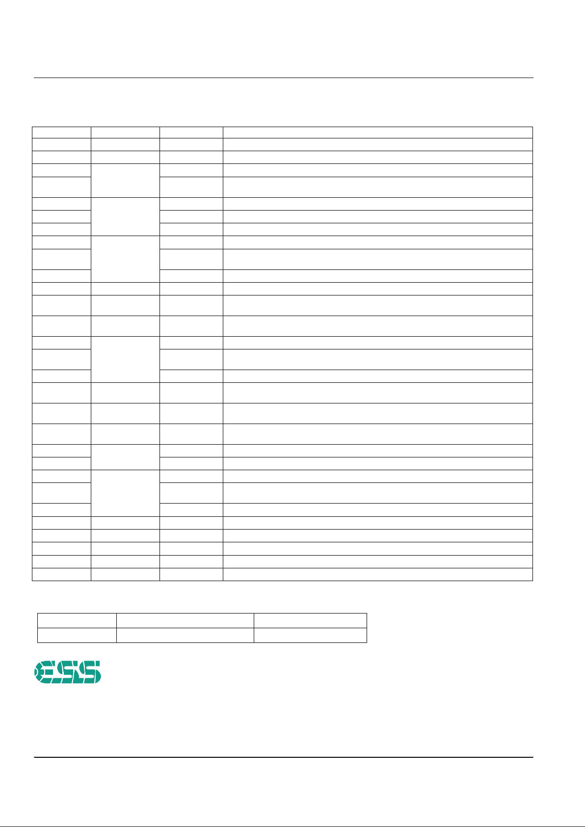
Name Pin Numbers I/O Descriptions
OSCO 65 O 49.152-MHz crystal output.
GD[0] 67 I/O Game port data input/output.
GD[1]
68
I/O Game port data input/output.
EDOUT O Data output to EEPROM data input. EDOUT goes active after power-on reset goes inactive
automatically after EEPROM cycle is complete.
GD[2]
69
I/O Game port data input/output.
EDIN I Data input from EEPROM data output.
VOLUP# I Hardware volume control enabled by PCI 52h [7] = 1 and PCI 52h [5] = 1.
GD[3]
70
I/O Game port data input/output.
ECLK O Clock output to EEPROM clock input. ECLK goes active after power-on reset and goes inactive
automatically after EEPROM cycle is complete.
VOLDN# I Hardware volume down control enabled by PCI 52h [7] = 1 and PCI 52h [5] = 1.
GD[4:7] 71:74 I Game port data input; internally pulled up to VDD.
SCLK1 76 I Primary AC-Link serial clock; enabled by setting Maestro_Base+36h [12] =1. Internally pulled up to
VDD.
SDFS1 77 O Primary AC-Link serial data frame sync; enabled by setting Maestro_Base+36h [12] =1. Internally
pulled up to VDD.
GT0#
78
O Grant to PCI master directly by enabling PCI 58h [0] = 1 and PCI 58h [11] = 1.
GS0 O Grant select 0 output to control external quick switch to grant PCI master phase by enabling PCIx2
arbiter bit PCI 58h [0] = 1 and PCI 58h [11] = 0.
GPIO1 I/O General-purpose input/output; internally pulled up to VDD.
SDO1 79 O Primary AC-Link serial data out enabled by setting Maestro_Base+36h[12]=1; internally pulled up to
VDD.
TXD 80 O MIDI transmit data output (default). Select as MIDI transmit output pin by enabling PCI 40h [3] = 1;
internally pulled up to VDD.
RXD 81 I MIDI receive data input (default). Select as MIDI receive input pin by enabling PCI 40h [3] = 1;
internally pulled down to GND.
PCREQ#
82
O Use as PC/PCI request output by setting PCI 50h [10:8] = 010.
GPIO13 I/O General-purpose input/output; internally pulled down to GND.
C24
83
O 24.576-MHz clock output for codec clock source.
SPDIFO O S/PDIF output; enabled by setting bit PCI 52h [8] = 1 and bit PCI 58h [1] = 1, and setting
Maestro_Base+38h[4]=1.
GPIO15 O General-purpose output-only; internally pulled up to VDD.
RST# 84 I Reset.
INT# 85 O Interrupt request.
PCICLK 87 I PCI bus clock.
GNT# 89 I PCI Bus master grant.
REQ# 90 O PCI Bus master request.
Table 1 ES1980 Pin Descriptions (Continued)
Part Number
Description Package
ES1980S PCI Audio-Modem Accelerator 100-pin LQFP
 Loading...