

Datasheet EN29F080-90TI, EN29F080-90T, EN29F080-70TI, EN29F080-70T, EN29F080-50TI Datasheet (EON)
...Page 1

4800 Great America Parkway, Suite 202 Tel: 408-235-8680
Santa Clara, CA 95054 Fax: 408-235-8685
1
EN29F080
Rev. C, Issue Date: 2001/ 07/05
FEATURES
•
5.0V ± 10%, single power supply operation
- Minimizes system level power requirements
•
Manufactured on 0.35 µm process technology
•
High performance
- Access times as fast as 45 ns
•
Low power consumption
- 25 mA typical active read current
- 30 mA typical program/erase current
- 1 µA typical standby current (standard access
time to active mode)
•
Flexible Sector Architecture:
- 16 uniform sectors of 64Kbytes each
- Supports full chip erase
- Individual sector erase supported
- Group sector protection:
Hardware method of locking of sector groups
to prevent any program or erase operations
within that sector group
Additionally, temporary Sector Group
Unprotect allows code changes in previously
locked sectors
•
High performance program/erase speed
- Byte program time: 10µs typical
- Sector erase time: 500ms typical
- Chip erase time: 16s typical
•
Low Standby Current
- 1µA CMOS standby current-typical
- 1mA TTL standby current
•
Low Power Active Current
- 30mA active read current
- 30mA program/erase current
•
JEDEC Standard program and erase
commands
•
JEDEC standard
DATA
polling and toggle
bits feature
•
Sector Unprotect Mode
•
Embedded Erase and Program Algorithms
•
Erase Suspend / Resume modes:
Read and program another Sector during
Erase Suspend Mode
•
0.35 µm double-metal double-poly
triple-well CMOS Flash Technology
•
Low Vcc write inhibit < 3.2V
•
>100K program/erase endurance cycle
•
Ready/Busy# output (RY/BY#)
- Provides a hardware method for detecting
program or erase cycle completion.
•
Hardware reset pin (Reset#)
- Resets internal state machine to read mode
GENERAL DESCRIPTION
The EN29F080 is a 8-Megabit, electrically erasable, read/write non-volatile flash m em ory. Organized
into 1024K words with 8 bits per word, the 8M of memory is arranged in eight uniform sectors of
64Kbytes each. Any byte can be programmed typically in 10µs. The EN29F080 features 5.0V
voltage read and write operation, with access times as fast as 45ns to eliminate the need f or WAIT
states in high-performance microprocessor systems.
The EN29F080 has separate Output Enable (
OE
), Chip Enable (CE), and Write Enable (
WE
)
controls, which eliminate bus contention issues. This device is designed to allow either single (or
multiple) Sector or full chip erase operation, where each Sector can be individually protected against
program/erase operations or temporarily unprotected to erase or program. The device can sustain a
minimum of 100K program/erase cycles on each Sector.
EN29F080
8 Megabit (1024K x 8-bit) Flash Memory
Page 2
4800 Great America Parkway, Suite 202 Tel: 408-235-8680
Santa Clara, CA 95054 Fax: 408-235-8685
2
EN29F080
Rev. C, Issue Date: 2001/ 07/05
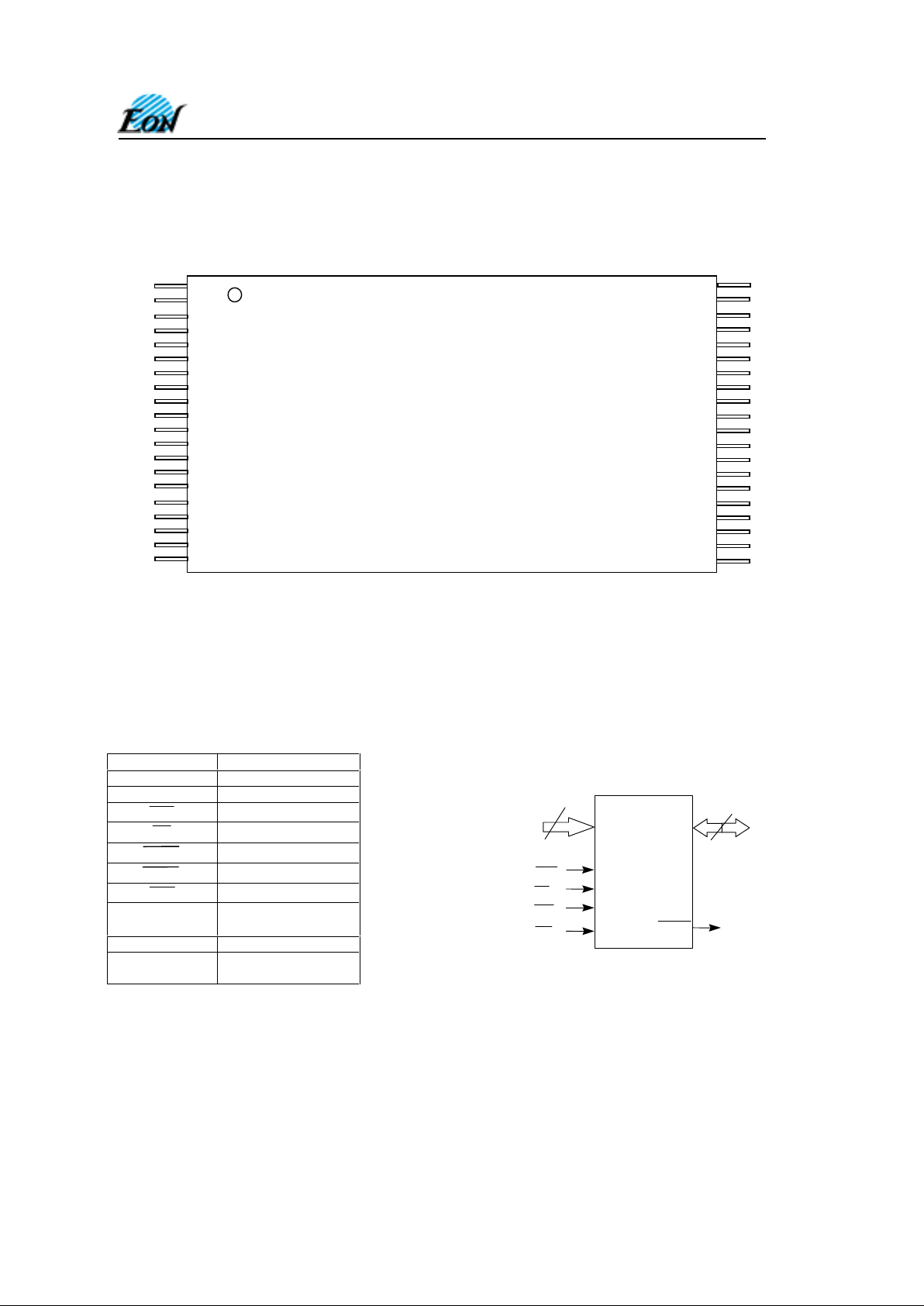
CONNECTION DIAGRAMS
TABLE 1. PIN DESCRIPTION FIGURE 1. LOGIC DIAGRAM
Pin Name Function
A0-A19 Addresses
DQ0-DQ7 Data Inputs/Outputs
CE
Chip Enable
OE
Output Enable
Hardware Reset Pin
Ready/Busy Output
WE
Write Enable
Vcc
Supply Voltage
(5V ± 10% )
Vss Ground
NC
Internally connected
pin
EN29F080
8
DQ0 - DQ7
A0 - A19
20
WE
CE
OE
RY/BY
Reset
1
2
3
4
5
6
7
8
9
10
11
12
13
14
15
16
17
18
19
20
40
39
38
37
36
35
34
33
32
31
30
29
28
27
26
25
24
23
22
21
Standard
TSOP
A19
A18
A17
A16
A15
A14
A13
A12
CE#
VCC
NC
RESET#
A11
A10
A9
A8
A7
A6
A5
A4
NC
NC
WE#
OE#
RY/BY#
DQ7
DQ6
DQ5
DQ4
VCC
VSS
VSS
DQ3
DQ2
DQ1
DQ0
A0
A1
A2
A3
Reset
RY/BY
Page 3
4800 Great America Parkway, Suite 202 Tel: 408-235-8680
Santa Clara, CA 95054 Fax: 408-235-8685
3
EN29F080
Rev. C, Issue Date: 2001/ 07/05
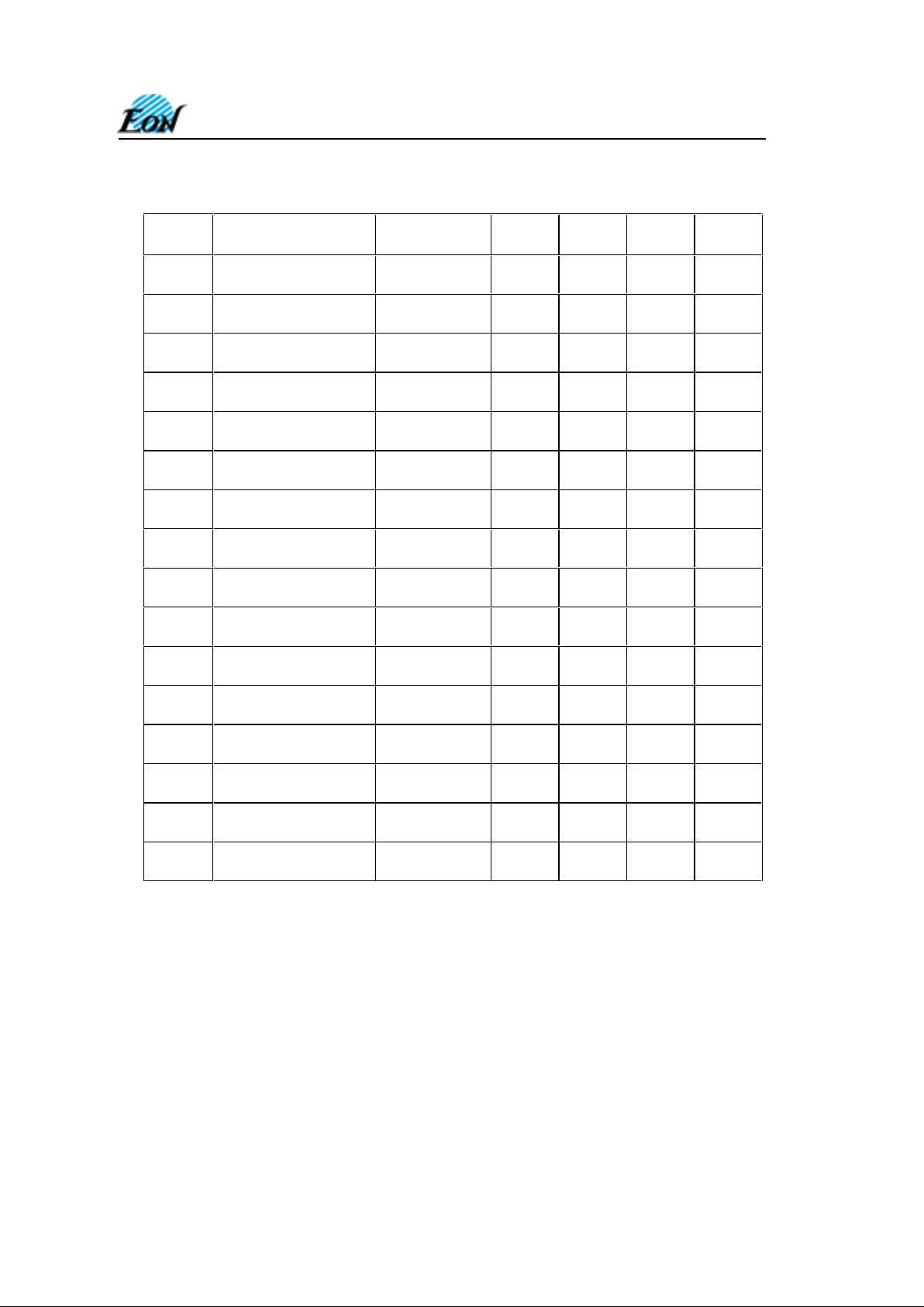
TABLE 2. SECTOR ARCHITECTURE
Sector ADDRESSES
SIZE (Kbytes) A19 A18 A17 A16
15 F0000h - FFFFFh 64 1 1 1 1
14 E0000h - EFFFFh 64 1 1 1 0
13 D0000h - DFFFFh 64 1 1 0 1
12 C0000h - CFFFFh 64 1 1 0 0
11 B0000h - BFFFFh 64 1 0 1 1
10 A0000h - AFFFFh 64 1 0 1 0
9 90000h - 9FFFFh 64 1 0 0 1
8 80000h - 8FFFFh 64 1 0 0 0
7 70000h - 7FFFFh 64 0 1 1 1
6 60000h - 6FFFFh 64 0 1 1 0
5 50000h – 5FFFFh 64 0 1 0 1
4 40000h – 4FFFFh 64 0 1 0 0
3 30000h – 3FFFFh 64 0 0 1 1
2 20000h - 2FFFFh 64 0 0 1 0
1 10000h - 1FFFFh 64 0 0 0 1
0 00000h - 0FFFFh 64 0 0 0 0
Page 4
4800 Great America Parkway, Suite 202 Tel: 408-235-8680
Santa Clara, CA 95054 Fax: 408-235-8685
4
EN29F080
Rev. C, Issue Date: 2001/ 07/05
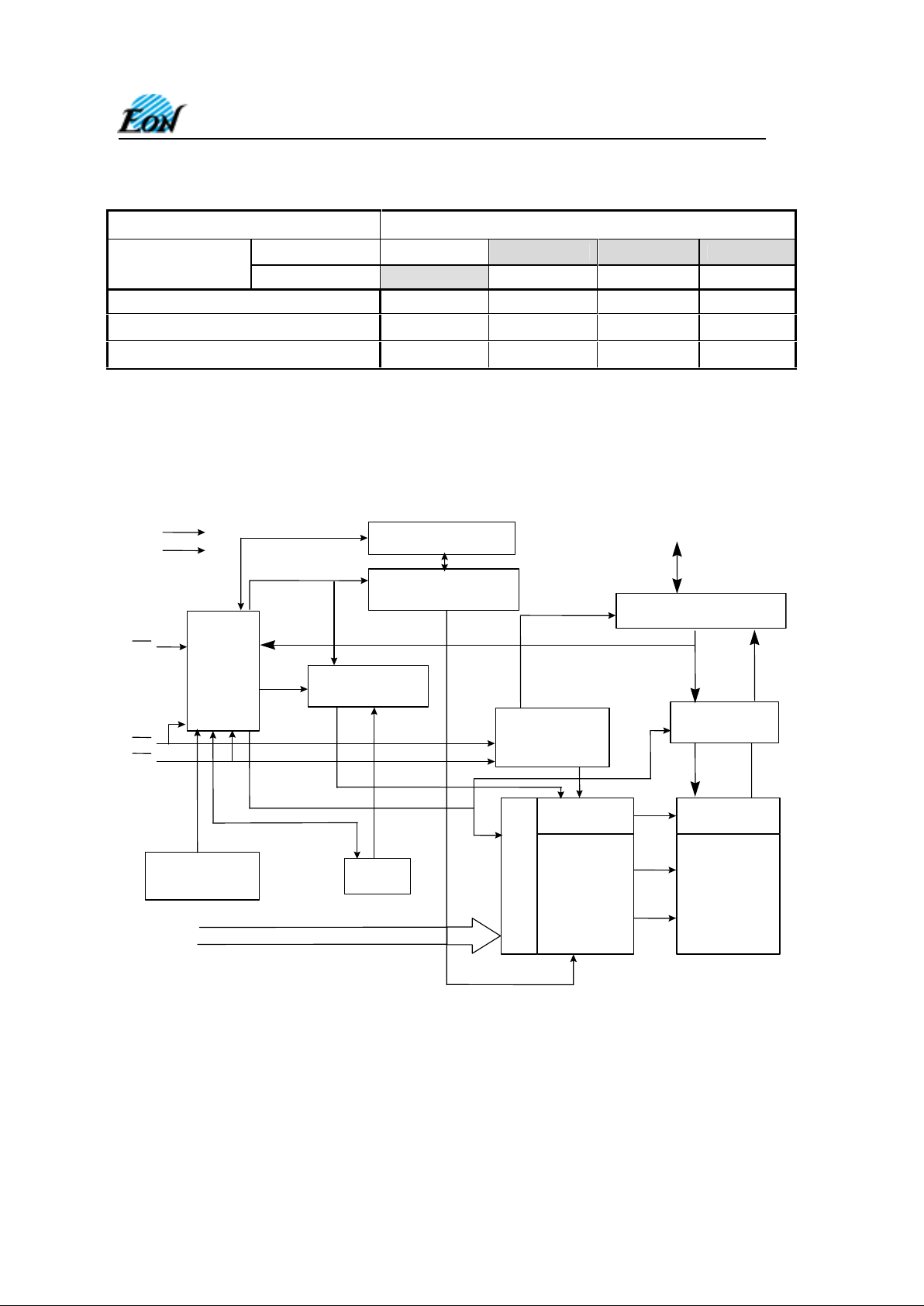
PRODUCT SELECTOR GUIDE
Product Number EN29F080
Vcc=5.0V ± 5%
-45
Speed Option
Vcc=5.0V ± 10%
-55 -70 -90
Max Access Time, ns (t
acc
) 45 55 70 90
Max CE# Access, ns (tce) 45 55 70 90
Max OE# Access, ns (toe) 25 30 30 35
BLOCK DIAGRAM
WE
CE
OE
State
Control
Command
Register
Erase Voltage Generator
Input/Output Buffers
Program Voltage
Generator
Chip Enable
Output Enable
Logic
Data Latch
Y-Decoder
X-Decoder
Y-Gating
Cell Matrix
Timer Vcc Detector
A0-A19
Vcc
Vss
DQ0-DQ7
Address Latch
Block Protect Switches
STB
STB
Page 5
4800 Great America Parkway, Suite 202 Tel: 408-235-8680
Santa Clara, CA 95054 Fax: 408-235-8685
5
EN29F080
Rev. C, Issue Date: 2001/ 07/05
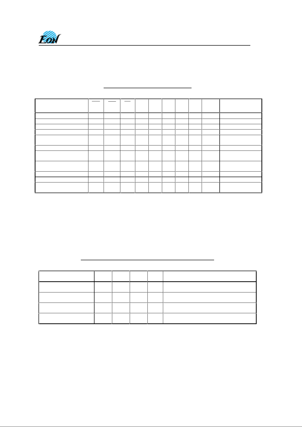
TABLE 3. OPERATING MODES
8M FLASH USER MODE TABLE
CE
WE
OE
A9 A8 A6 A1 A0 Ax/y DQ(0-7)
USER MODE
STANDBY H X X X X X X X X HI-Z
READ L H L A9 A8 A6 A1 A0 Ax/y DQ(0-7)
OUTPUT DISABLE L H H A9 A8 A6 A1 A0 Ax/y HI-Z
READ
MANUFACTURE ID
L H L VID L/H L L L X MANUFACTURE
ID
READ DEVICE ID L H L VID L/H L L H X DEVICE ID(T/B)
VERIFY SECTOR
PROTECT
L H L VID X L H L X CODE
ENABLE SECTOR
PROTECT
L L VID VID X L X X X X
SECTOR UNPROTECT L L VID VID X H H L X X
WRITE L L H A9 A8 A6 A1 A0 Ax/y DIN(0-7)
TEMPORARY SECTOR
UNPROTECT
X X X X X X X X X X
NOTES:
1) L = V
IL
, H = VIH, VID = 11.5V ± 0.5V
2) X = Don’t care, either V
IH
or VIL
TABLE 4. DEVICE IDENTIFICTION
8M FLASH MANUFACTURER/DEVICE ID TABLE
A8 A6 A1 A0 DQ(7-0)
HEX
READ CONTINUATION
MANUFACTURER ID
L L L L MANUFACTURER ID
7F
READ
MANUFACTURER ID
H L L L MANUFACTURER ID
1C
READ CONTINUATION
DEVICE ID
L L L H DEVICE ID
7F
READ DEVICE ID H L L H DEVICE ID
08
Page 6

4800 Great America Parkway, Suite 202 Tel: 408-235-8680
Santa Clara, CA 95054 Fax: 408-235-8685
6
EN29F080
Rev. C, Issue Date: 2001/ 07/05
USER MODE DEFINITIONS
Standby Mode
The EN29F080 has a CMOS-com patible standby mode, which reduces the
current to < 1µA (typical).
It is placed in CMOS-compatible standby when the RESET# and
CE
pin is at VCC ± 0.5. The device
also has a TTL-com patible standby mode, which reduces the m aximum V
CC
current to < 1mA. It is
placed in TTL-com patible standby when the
CE
pin is at VIH. When in standby modes , the outputs
are in a high-impedance state independent of the
OE
input.
Read Mode
The device is automatically set to reading array data after device power-up. No commands are required to
retrieve data. The device is also ready to read array data after completing an Embedded Program or
Embedded Erase algorithm.
After the device accepts an Erase Suspend command, the device enters the Erase Suspend mode. The
system can read array data using the standard read timings, except that if it reads at an address within
erase-suspended sectors, the device outputs status data. After completing a programming operation in
the Erase Suspend mode, the system may once again read array data with the same exception. See
“Erase Suspend/Erase Resume Commands” for more additional information.
The system
must issue the reset command to re-enable the device for reading array data if DQ5 goes
high, or while in the autoselect mode. See the “Reset Command” additional details.
Output Disable Mode
When the
CE
or OE pin is at a logic high level (VIH), the output from the EN29F080 is disabled.
The output pins are placed in a high impedance state.
Auto Select Identification Mode
The autoselect mode provides manufacturer and device identification, and sector protection
verification, through identifier codes output on DQ7–DQ0. This mode is primarily intended for
programming equipment to automatically match a device to be programmed with its corresponding
programming algorithm. However, the autoselect codes can also be accessed in-system through the
command register.
When using programming equipment, the autoselect mode requires V
ID
(10.5 V to 11.5 V) on
address pin A9. Address pins A6, A1, and A0 must be as shown in Autoselect Codes (High Voltage
Method) table. In addition, when verifying sector protection, the sector address must appear on the
appropriate highest order address bits. Refer to the corresponding Sector Address Tables. The
Command Definitions table shows the remaining address bits that are don’t-care. When all
necessary bits have been set as required, the programming equipment may then read the
corresponding identifier code on DQ7–DQ0.
To access the autoselect codes in-system; the host system can issue the autoselect command via
the command register, as shown in the Command Definitions table. This method does not require
V
ID
. See “Command Definitions” for details on using the autoselect mode.
Page 7
4800 Great America Parkway, Suite 202 Tel: 408-235-8680
Santa Clara, CA 95054 Fax: 408-235-8685
7
EN29F080
Rev. C, Issue Date: 2001/ 07/05
Write Mode
Programming is a four-bus-cycle operation. The program command sequence is initiated by writing two
unlock write cycles, followed by the program set-up command. The program address and data are written
next, which in turn initiate the Embedded Program algorithm. The system is
not required to provide further
controls or timings. The device automatically provides internally generated program pulses and verifies
the programmed cell margin. The Command Definitions in Table 5 show the address and data
requirements for the byte program command sequence.
When the Embedded Program algorithm is complete, the device then returns to reading array data and
addresses are no longer latched. The system can determine the status of the program operation by using
DQ7 or DQ6. See “Write Operation Status” for information on these status bits.
Any commands written to the device during the Embedded Program Algorithm are ignored.
Programming is allowed in any sequence and across sector boundaries. A bit cannot be programmed
from a “0” back to a “1”. Attempting to do so may halt the operation and set DQ5 to “1”, or cause the
Data# Polling algorithm to indicate the operation was successful. However, a succeeding read will show
that the data is still “0”. Only erase operations can convert a “0” to a “1”.
Sector Group Protection/Unprotection
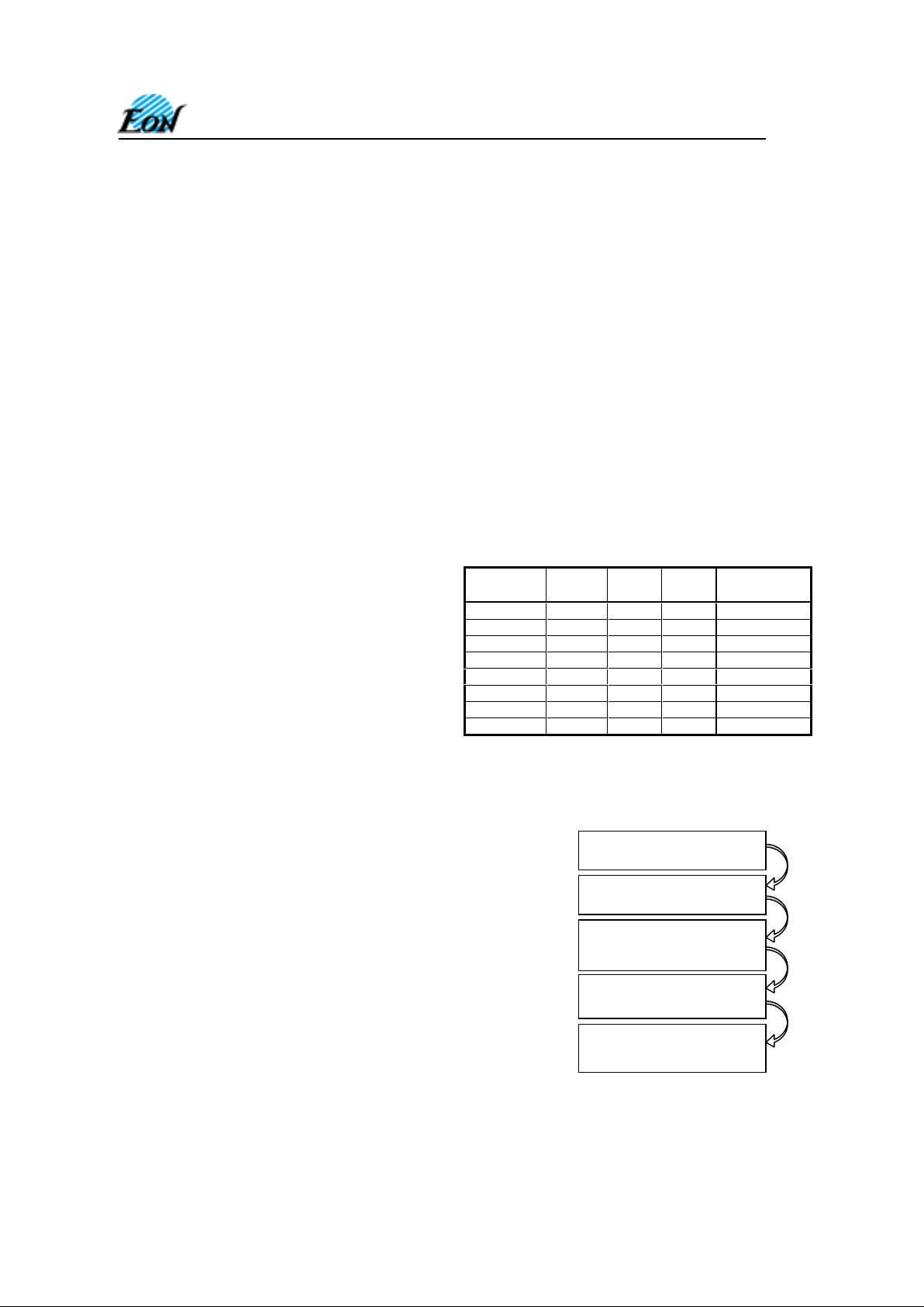
The hardware sector protection feature disables
both program and erase operations in any sector.
Each group consists of two adjacent sectors. The
Sector Group Addresses table shows how the
sectors are grouped, and the address range that
each sector group contains. The hardware sector
group unprotection feature re-enables both program
and erase operations in previously protected sector
groups.
Sector protection/unprotection must be implemented using programming equipment. The procedure requires a high voltage (V
ID) on address pin A9 and the control pins. Details on this method are provided in
a supplement, which can be obtained by contacting a representative of Eon Silicon Devices, Inc.
Temporary Sector Group Unprotect
This feature allows temporary unprotection of previously protected
sector groups to change data while in-system. The Sector Group
Unprotect mode is activated by setting the RESET# pin to V
ID
(10.5 V
to 11.5 V). During this mode, formerly protected sector groups can be
programmed or erased by simply selecting the sector group
addresses. Once V
ID
is removed from the RESET# pin, all the
previously protected sector groups are protected again. See
accompanying figure and timing diagrams for more details.
Sector Group Addresses
Sector
Group
A19 A18 A17 Sectors
SGA0 0 0 0 SA0-SA1
SGA1 0 0 1 SA2-SA3
SGA2 0 1 0 SA4-SA5
SGA3 0 1 1 SA6-SA7
SGA4 1 0 0 SA8-SA9
SGA5 1 0 1 SA10-SA11
SGA6 1 1 0 SA12-SA13
SGA7 1 1 1 SA14-SA15
Start
Reset#=VID (note 1)
Perform Erase or Program
Operations
Reset#=VIH
Temporary Sector Group
Unprotect Completed
(note 2)
Notes:
1. All protected sector groups unprotected.
2. Previously protected sector groups
protected again.
3. V
IH
= Logic High
Page 8

4800 Great America Parkway, Suite 202 Tel: 408-235-8680
Santa Clara, CA 95054 Fax: 408-235-8685
8
EN29F080
Rev. C, Issue Date: 2001/ 07/05
Hardware Data protection
The command sequence requirement of unlock cycles for programming or erasing provides data
protection against inadvertent writes as seen in the Command Definitions table. Additionally, the
following hardware data protection measures prevent accidental erasure or programming, which might
otherwise be caused by false system level signals during Vcc power up and power down transitions, or
from system noise.
Low VCC Write Inhibit
When Vcc is less than V
LKO
, the device does not accept any write cycles. This protects data during Vcc
power up and power down. The command register and all internal program/erase circuits are disabled,
and the device resets. Subsequent writes are ignored until Vcc is greater than V
LKO
. The system must
provide the proper signals to the control pins to prevent unintentional writes when Vcc is greater than
V
LKO
.
Write Pulse “Glitch” protection
Noise pulses of less than 5 ns (typical) on
OE
, CE or
WE
do not initiate a write cycle.
Logical Inhibit
If CE=VIH or WE=VIH, writing is inhibited. To initiate a write cycle, CE and
WE
must be a logical
“zero”. If
CE
, WE, and OE are all logical zero (not recommended usage), it will be cons idered a
write.
Power-up Write Inhibit
During power-up, the device automatically resets to READ mode and loc ks out write cycles. Even
with
CE
= VIL, WE = VIL and OE = VIH, the device will not accept com mands on the r ising edge of
WE
.
Page 9
4800 Great America Parkway, Suite 202 Tel: 408-235-8680
Santa Clara, CA 95054 Fax: 408-235-8685
9
EN29F080
Rev. C, Issue Date: 2001/ 07/05
COMMAND DEFINITIONS
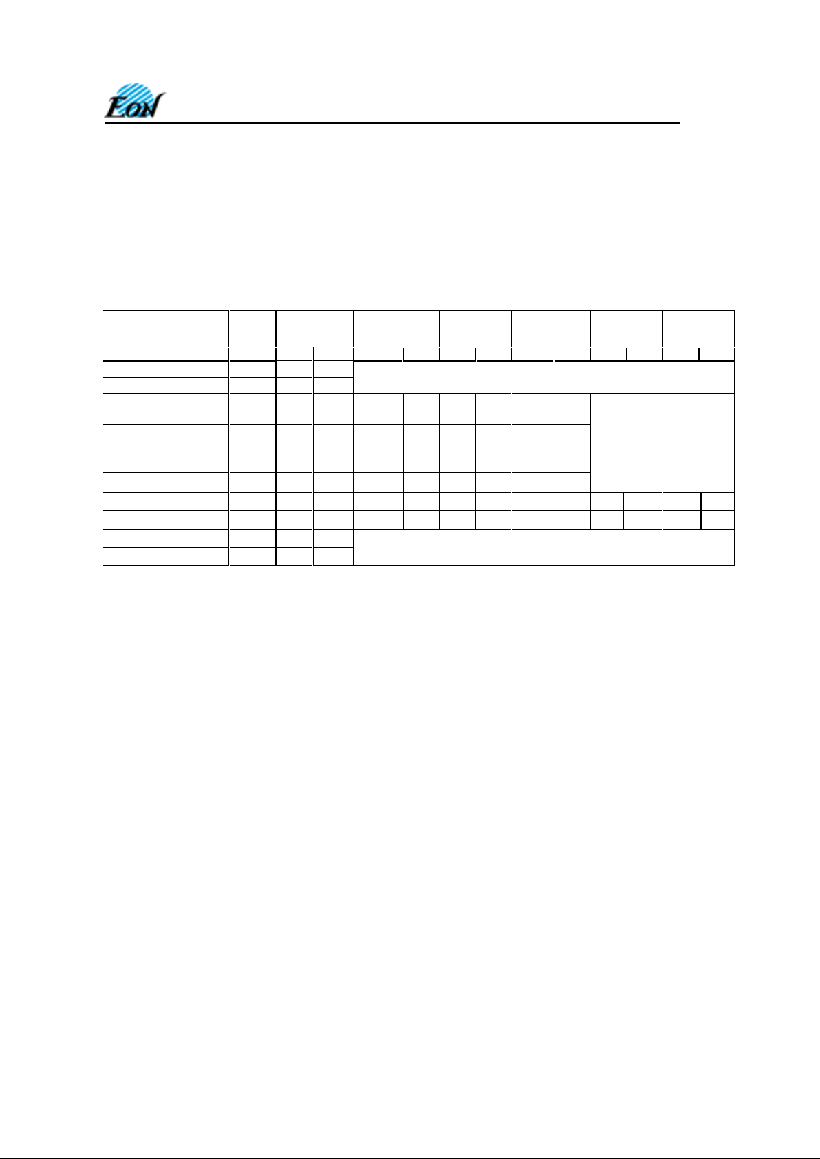
The operations of the EN29F080 are selected by one or m ore commands written into the command
register to perform Read/Reset Mem ory, Read ID, Read Sector Protection, Program , Sector Eras e,
Chip Erase, Erase Suspend and Erase Resume. Commands are made up of data sequences
written at specific addresses via the c omm and register . The sequences for the specified operation
are defined in the Command Def initions table (T able 5) . Incorrec t address es, incorrec t data values
or improper sequences will reset the device to Read Mode.
Table 5. EN29F080 Command Definitions
1
st
Write Cycle
2
nd
Write Cycle
3
rd
Write Cycle
4
th
Write Cycle
5
th
Write Cycle
6
th
Write Cycle
Command
Sequence
Read/Reset
Cycles
Addr Data Addr Data Addr Data Addr Data Addr Data Addr Data
Reset
1
XXXh F0h
Read
4
RA RD
AutoSelect
Manufacturer ID
4
555h AAh 2AAh 55h 555h 90h X100h 1c
AutoSelect Device ID
4
555h AAh 2AAh 55h 555h 90h X101h 08
AutoSelect Sector
Protect Verify
4
555h AAh 2AAh 55h 555h 90h
BA &
02h
00h/
01h
Byte Program
4
555h AAh 2AAh 55h 555h A0h PA PD
Chip Erase
6
555h AAh 2AAh 55h 555h 80h 555h AAh 2AAh 55h 555h 10h
Sector Erase
6
555h AAh 2AAh 55h 555h 80h 555h AAh 2AAh 55h BA 30h
Sector Erase Suspend
1
xxxh B0h
Sector Erase Resume
1
xxxh 30h
RA = Read Address: address of the memory location to be read. This one is a read cycle.
RD = Read Data: data read from locat i on RA duri ng Read operation. This one is a read cycle.
PA = Program Address: address of the memory loc ation to be programmed
PD = Program Data: data to be programmed at location PA
BA = Sector Address: address of the Sector to be erased or veri f i ed. Address bits A17-A13 uniquel y s el ect any Sector.
Reading Array Data
The device is automatically set to reading array data after power up. No commands are required to
retrieve data. The device is also ready to read array data after completing an Embedded Program or
Embedded Erase algorithm.
Following an Erase Suspend command, Erase Suspend mode is entered. The system can read array data
using the standard read timings, with the only difference in that if it reads at an address within erase
suspended sectors, the device outputs status data. After completing a programming operation in the Erase
Suspend mode, the system may once again read array data with the same exception.
The Reset command must be issued to re-enable the device for reading array data if DQ5 goes high, or while
in the autoselect mode. See next section for details on Reset.
Reset Command
Writing the reset command to the device resets the device to reading array data. Address bits are don’tcare for this command.
The reset command may be written between the sequence cycles in an erase command sequence before
erasing begins. This resets the device to reading array data. Once erasure begins, however, the device
ignores reset commands until the operation is complete. The reset command may be written between the
sequence cycles in a program command sequence before programming begins. This resets the device to
reading array data (also applies to programming in Erase Suspend mode). Once programming begins,
however, the device ignores reset commands until the operation is complete.
Page 10

4800 Great America Parkway, Suite 202 Tel: 408-235-8680
Santa Clara, CA 95054 Fax: 408-235-8685
10
EN29F080
Rev. C, Issue Date: 2001/ 07/05
The reset command may be written between the sequence cycles in an autoselect command sequence.
Once in the autoselect mode, the reset command
must be written to return to reading array data.
If DQ5 goes high during a program or erase operation, writing the reset command returns the device to
reading array data (also applies during Erase Suspend).
Autoselect Command Sequence
The autoselect command sequence allows the host system to access the manufacturer and devices
codes, and determine whether or not a sector is protected. The Command Definitions table shows the
address and data requirements. This is an alternative method which is intended for PROM programmers
and requires V
ID
on address bit A9.
Two unlock cycles followed by the autoselect command initiate the autoselect command sequence.
Autoselect mode is then entered and the system may read at any address any number of times, without
needing another command sequence.
The system must write the reset command to exit the autoselect mode and return to reading array data.
Byte Programming Command
Programming the EN29F080 is performed on a byte-by-byte basis using a four bus-cycle operation
(two unlock write cycles followed by the Program Setup command and Program Data Write cycle).
When the program command is executed, no additional CPU controls or timings are necessary. An
internal timer terminates the program operation automatically. Address is latched on the falling edge
of
CE
or
WE
, whichever is last; data is latched on the rising edge of CE or
WE
, whichever is first.
The program operation is completed when EN29F080 returns the equivalent data to the programmed
location.
Programming status may be checked by sampling data on DQ7 (
DATA
polling) or on DQ6 (toggle
bit). Changing data from 0 to 1 requires an erase operation. When programming time limit is
exceeded, DQ5 will produce a logical “1” and a Reset command can return the device to Read mode.
Chip Erase Command
Chip erase is a six-bus-cycle operation. The chip erase command sequence is initiated by writing two
unlock cycles, followed by a set-up command. Two additional unlock write cycles are then followed by the
chip erase command, which in turn invokes the Embedded Erase algorithm. The device does
not require
the system to preprogram prior to erase. The Embedded Erase algorithm automatically preprograms and
verifies the entire memory for an all zero data pattern prior to electrical erase. The system is not required
to provide any controls or timings during these operations. The Command Definitions table shows the
address and data requirements for the chip erase command sequence.
Any commands written to the chip during the Embedded Erase algorithm are ignored.
The system can determine the status of the erase operation by using DQ7, DQ6, or DQ2. See “Write
Operation Status” for information on these status bits. When the Embedded Erase algorithm is complete,
the device returns to reading array data and addresses are no longer latched.
Flowchart 4 illustrates the algorithm for the erase operation. See the Erase/Program Operations tables in
“AC Characteristics” for parameters, and to the Chip/Sector Erase Operation Timings for timing
waveforms.
Page 11

4800 Great America Parkway, Suite 202 Tel: 408-235-8680
Santa Clara, CA 95054 Fax: 408-235-8685
11
EN29F080
Rev. C, Issue Date: 2001/ 07/05
Sector Erase Command Sequence
Sector erase is a six bus cycle operation. The sector erase command sequence is initiated by writing two
un-lock cycles, followed by a set-up command. Two additional unlock write cycles are then followed by
the address of the sector to be erased, and the sector erase command. The Command Definitions table
shows the address and data requirements for the sector erase command sequence.
This device does not support multiple sector erase commands. Sector Erase operation will
commence immediately after the first 30h command is written. The first sector erase operation must
finish before another sector erase command can be given.
Once the sector erase operation has begun, only the Erase Suspend command is valid. All other
commands are ignored.
When the Embedded Erase algorithm is complete, the device returns to reading array data and addresses
are no longer latched. The system can determine the status of the erase operation by using DQ7, DQ6, or
DQ2. Refer to “Write Operation Status” for information on these status bits. Flowchart 4 illustrates the
algorithm for the erase operation. Refer to the Erase/Program Operations tables in the “AC
Characteristics” section for parameters, and to the Sector Erase Operations Timing diagram for timing
waveforms.
Erase Suspend / Resume Command
The Erase Suspend command allows the system to interrupt a sector erase operation and then read data
from, or program data to, any sector not selected for erasure. This command is valid only during the
sector erase operation. The Erase Suspend command is ignored if written during the chip erase operation
or Embedded Program algorithm. Addresses are don’t-cares when writing the Erase Suspend command.
When the Erase Suspend command is written during a sector erase operation, the device requires a
maximum of 20 µs to suspend the erase operation.
After the erase operation has been suspended, the system can read array data from or program data to
any sector not selected for erasure. (The device “erase suspends” all sectors selected for erasure.)
Normal read and write timings and command definitions apply. Reading at any address within erasesuspended sectors produces status data on DQ7–DQ0. The system can use DQ7, or DQ6 and DQ2
together, to determine if a sector is actively erasing or is erase-suspended. See “Write Operation Status”
for information on these status bits.
After an erase-suspended program operation is complete, the system can once again read array data
within non-suspended sectors. The system can determine the status of the program operation using the
DQ7 or DQ6 status bits, just as in the standard program operation. See “Write Operation Status” for more
information.
The system must write the Erase Resume command (address bits are don’t-care) to exit the erase
suspend mode and continue the sector erase operation. Further writes of the Resume command are
ignored. Another Erase Suspend command can be written after the device has resumed erasing.
Page 12

4800 Great America Parkway, Suite 202 Tel: 408-235-8680
Santa Clara, CA 95054 Fax: 408-235-8685
12
EN29F080
Rev. C, Issue Date: 2001/ 07/05
WRITE OPERATION STATUS
DQ7
DAT
A
Polling
The EN29F080 provides
DATA
Polling on DQ7 to indicate to the host system the status of the
embedded operations. The
DATA
Polling feature is active during the Byte Programm ing, Sector
Erase, Chip Erase, Erase Suspend and sector erase time-out window. (See Table 6)
When the Byte Programming is in progress, an attempt to read the device will produce the
complement of the data last written to DQ7. Upon the completion of the Byte Programming, an
attempt to read the device will produce the tr ue data last written to DQ7. For the Byte Programm ing,
DATA
polling is valid after the rising edge of the fourth WE or CEpulse in the four-cycle sequence.
When the em bedded Erase is in progress, an attempt to read the device will produce a “0” at the
DQ7 output. Upon the completion of the em bedded Erase, the device will produce the “1” at the DQ7
output during the read. For Chip Erase, the
DATA
polling is valid after the rising edge of the six th
WE
or CE pulse in the six-c ycle sequence. For Sector Erase,
DATA
polling is valid after the last
rising edge of the sector erase
WE
or CEpulse.
DATA
Polling must be performed at any address within a sector that is being programmed or erased
and not a protected sector. Otherwise,
DATA
polling may give an inaccurate result if the address
used is in a protected sector.
Just prior to the com pletion of the embedded operations, DQ7 may change asynchronously when the
output enable (
OE
) is low. This means that the device is driving status information on DQ7 at one
instant of time and valid data at the next instant of time. Depending on when the system samples the
DQ7 output, it may read the status of valid data. Even if the device has c ompleted the embedded
operations and DQ7 has a valid data, the data output on DQ0-DQ6 may be still invalid. The valid
data on DQ0-DQ7 will be read on the subsequent read attempts.
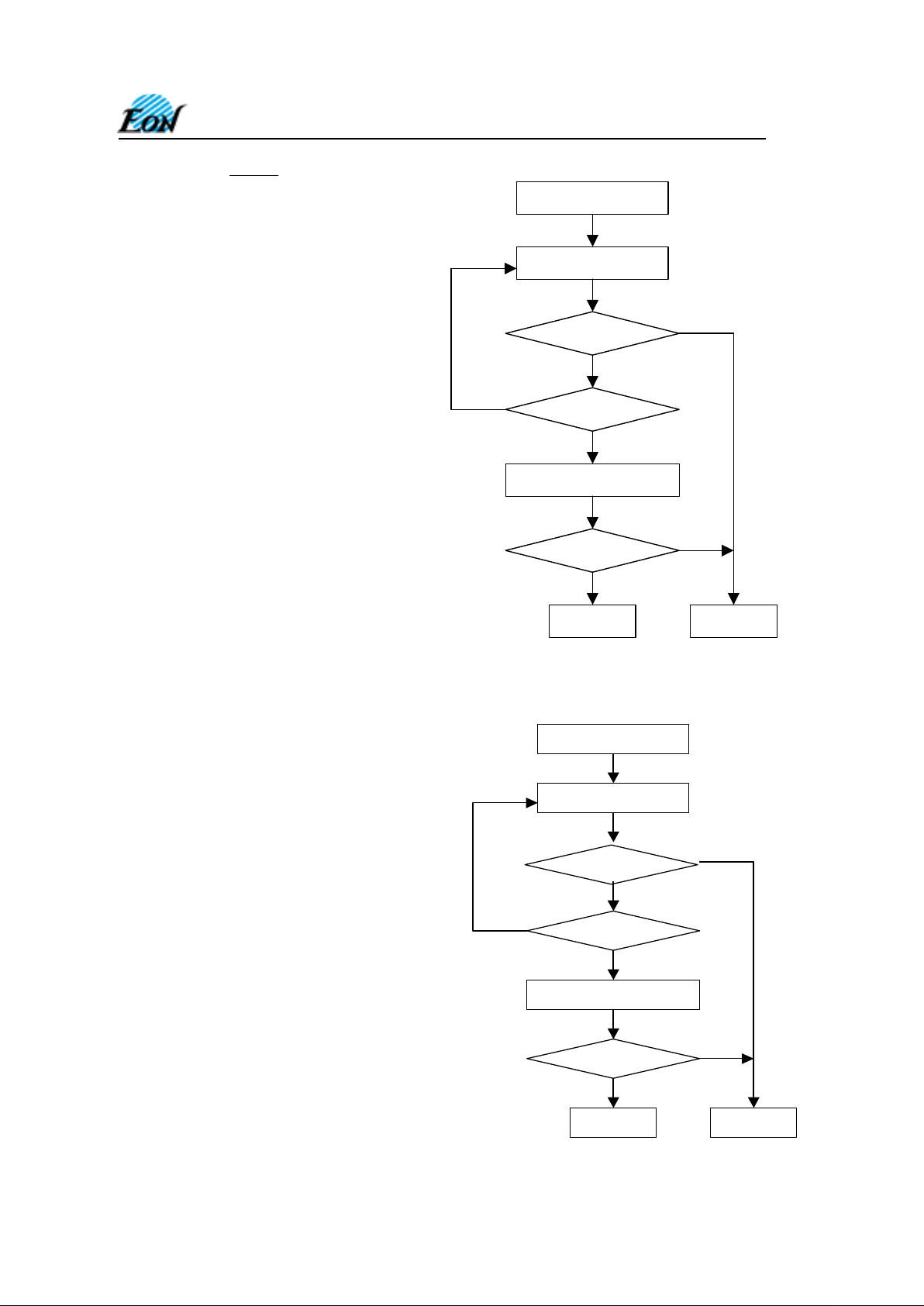
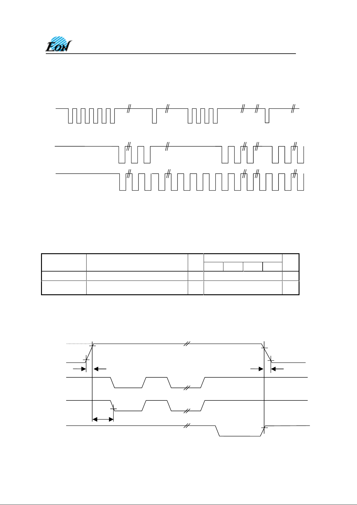
The flowchart for
DATA
Polling (DQ7) is shown on Flowchart 5. The
DATA
Polling (DQ7) timing
diagram is shown in Figure 8.
RY/BY: Ready/Busy
The RY/BY is a dedicated, open-drain output pin that indicates whether an Embedded Algorithm is in
progress or complete. The RY/BY status is valid after the rising edge of the final WE pulse in the
command sequence. Since RY/BY is an open-drain output, several RY/BY pins can be tied together
in parallel with a pull-up resistor to Vcc.
In the output is low, signifying Busy, the device is actively erasing or programming. This includes
programming in the Erase Suspend mode. If the output is high, signifying the Ready, the device is
ready to read array data (including during the Erase Suspend mode), or is in the standby mode.
DQ6
Toggle Bit I
The EN29F080 provides a “Toggle Bit” on DQ6 to indicate to the host system the status of the
embedded programming and erase operations. (See Table 6)
During an embedded Program or Erase operation, suc cessive attem pts to read data from the device
at any address (by toggling
OE
or CE) will result in DQ6 toggling between “zero” and “one”. Once
Page 13

4800 Great America Parkway, Suite 202 Tel: 408-235-8680
Santa Clara, CA 95054 Fax: 408-235-8685
13
EN29F080
Rev. C, Issue Date: 2001/ 07/05
the embedded Program or Erase operation is com plete, DQ6 will stop toggling and valid data will be
read on the next successive attem pts. During Byte Programming, the Toggle Bit is valid after the
rising edge of the fourth
WE
pulse in the four-cycle sequence. For Chip Erase, the T oggle Bit is valid
after the rising edge of the sixth-cycle sequence. For Sector Erase, the T oggle Bit is valid after the
last rising edge of the Sector Eras e
WE
pulse. The Toggle Bit is also ac tive dur ing the s ec tor er as e
time-out window.
In Byte Programming, if the s ector being written to is protected, DQ 6 will toggles for about 2 µs, then
stop toggling without the data in the sector having changed. In Sector Erase or Chip Erase, if all
selected blocks are protec ted, DQ6 will toggle for about 100 µs. The chip will then return to the read
mode without changing data in all protected blocks.
Toggling either
CE
or OE will cause DQ6 to toggle.
The flowchart for the T oggle Bit (DQ6) is shown in Flowchart 6. The Toggle Bit timing diagram is
shown in Figure 9
.
DQ5 Exceeded Timing Limits
DQ5 indicates whether the program or erase time has exceeded a specified internal pulse count limit.
Under these conditions DQ5 produces a “1.” This is a failure condition that indicates the program or erase
cycle was not successfully completed.
The DQ5 failure condition may appear if the system tries to program a “1” to a location that is previously
programmed to “0.” Only an erase operation can change a “0” back to a “1.” Under this condition, the
device halts the operation, and when the operation has exceeded the timing limits, DQ5 produces a “1.”
Under both these conditions, the system must issue the reset command to return the device to reading
array data.
DQ3 Sector Erase Timer
After writing a sector erase command sequence, the output on DQ3 can be used to determine whether or
not an erase operation has begun. (The sector erase timer does not apply to the chip erase command.)
When sector erase starts, DQ3 switches from “0” to “1.” This device does not support multiple sector
erase command sequences so it is not very meaningful. Future devices may support this feature.
DQ2 Erase Toggle Bit
The “Toggle Bit” on DQ2, when used with DQ6, indicates whether a particular sector is actively erasing
(that is, the Embedded Erase algorithm is in progress), or whether that sector is erase-suspended. Toggle
Bit II is valid after the rising edge of the final WE# pulse in the command sequence. DQ2 toggles when
the system reads at addresses within those sectors that have been selected for erasure. (The system may
use either OE# or CE# to control the read cycles.) But DQ2 cannot distinguish whether the sector is
actively erasing or is erase-suspended. DQ6, by comparison, indicates whether the device is actively
erasing, or is in Erase Suspend, but cannot distinguish which sectors are selected for era-sure. Thus,
both status bits are required for sector and mode information. Refer to Table 5 to compare outputs for
DQ2 and DQ6.
Flowchart 6 shows the toggle bit algorithm, and the section “DQ2: Toggle Bit” explains the algorithm. See
also the “DQ6: Toggle Bit I” subsection. Refer to the Toggle Bit Timings figure for the toggle bit timing
diagram. The DQ2 vs. DQ6 figure shows the differences between DQ2 and DQ6 in graphical form.
Reading Toggle Bits DQ6/DQ2
Refer to Flowchart 6 for the following discussion. Whenever the system initially begins reading toggle bit
status, it must read DQ7–DQ0 at least twice in a row to determine whether a toggle bit is toggling.
Typically, a system would note and store the value of the toggle bit after the first read. After the second
read, the system would compare the new value of the toggle bit with the first. If the toggle bit is not
Page 14
4800 Great America Parkway, Suite 202 Tel: 408-235-8680
Santa Clara, CA 95054 Fax: 408-235-8685
14
EN29F080
Rev. C, Issue Date: 2001/ 07/05
toggling, the device has completed the program or erase operation. The system can read array data on
DQ7–DQ0 on the following read cycle.
However, if after the initial two read cycles, the system determines that the toggle bit is still toggling, the
sys-tem also should note whether the value of DQ5 is high (see the section on DQ5). If it is, the system
should then determine again whether the toggle bit is toggling, since the toggle bit may have stopped
toggling just as DQ5 went high. If the toggle bit is no longer toggling, the device has successfully
completed the program or erase operation. If it is still toggling, the device did not complete the operation
successfully, and the system must write the reset command to return to reading array data.
The remaining scenario is that the system initially determines that the toggle bit is toggling and DQ5 has
not gone high. The system may continue to monitor the toggle bit and DQ5 through successive read
cycles, determining the status as described in the previous paragraph. Alternatively, it may choose to
perform other system tasks. In this case, the system must start at the beginning of the algorithm when it
returns to determine the status of the operation (top of Flowchart 6).
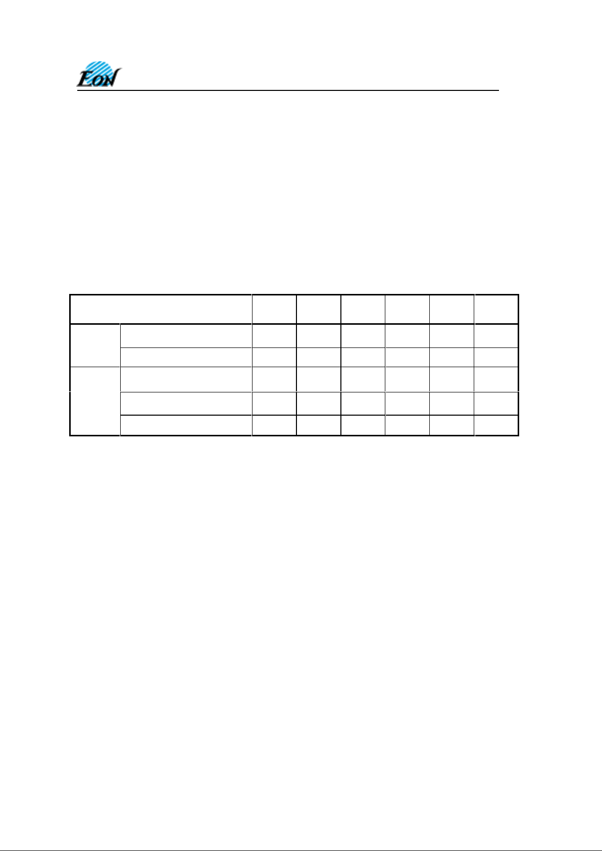
Write Operation Status
Operation DQ7 DQ6 DQ5 DQ3 DQ2
RY/BY
#
Embedded Program
Algorithm
DQ7# Toggle 0 N/A
No
toggle
0
Standard
Mode
Embedded Erase Algorithm 0 Toggle 0 1 Toggle 0
Reading within Erase
Suspended Sector
1
No
Toggle
0 N/A Toggle 1
Reading within Non-Erase
Suspended Sector
Data Data Data Data Data 1
Erase
Suspend
Mode
Erase-Suspend Program DQ7# Toggle 0 N/A N/A 0
Page 15
4800 Great America Parkway, Suite 202 Tel: 408-235-8680
Santa Clara, CA 95054 Fax: 408-235-8685
15
EN29F080
Rev. C, Issue Date: 2001/ 07/05
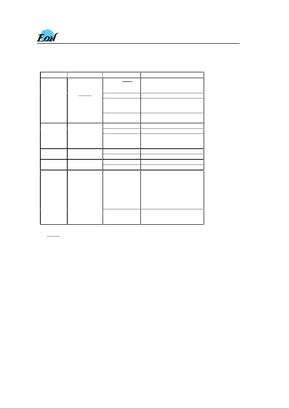
Table 6. Status Register Bits
DQ Name Logic Level Definition
‘1’
Erase Complete or
erase Sector in Erase
suspend
‘0’ Erase On-Going
DQ7
Program Complete or
data of non-erase Sector
during Erase Suspend
7
DATA
POLLING
DQ7
Program On-Going
‘-1-0-1-0-1-0-1-’ Erase or Program On-going
DQ6 Read during Erase Suspend
6
TOGGLE
BIT
‘-1-1-1-1-1-1-1-‘
Erase Complete
‘1’ Program or Erase Error
5 ERROR BIT
‘0’ Program or Erase On-going
‘1’ Erase operation start
3
ERASE
TIME BIT
‘0’ Erase timeout period on-going
‘-1-0-1-0-1-0-1-’
Chip Erase, Erase or Erase
suspend on currently
addressed
Sector. (When DQ5=1, Erase
Error due to currently
addressed Sector. Program
during Erase Suspend on-
going at current address
2
TOGGLE
BIT
DQ2
Erase Suspend read on
non Erase Suspend Sector
Notes:
DQ7
DATA
Polling: indicates t he P/E C status check during Program or Erase, and on completion before checking bits
DQ5 for Program or Erase Succ ess.
DQ6 Toggle Bit: remains at constant level when P/E C operations are c omplete or erase suspend is ac knowledged.
Successive reads output complementary data on DQ6 while program ming or Erase operation are on-going.
DQ5 Error Bit: set to “1’ i f failure in programming or erase
DQ3 Sector Erase Command Time out Bit: Operati on has started. Only possible command is Erase suspend (ES).
DQ2 Toggle Bit: indicates the Erase status and allows identi fication of the erased Sect or.
Page 16
4800 Great America Parkway, Suite 202 Tel: 408-235-8680
Santa Clara, CA 95054 Fax: 408-235-8685
16
EN29F080
Rev. C, Issue Date: 2001/ 07/05
EMBEDDED ALGORITHMS
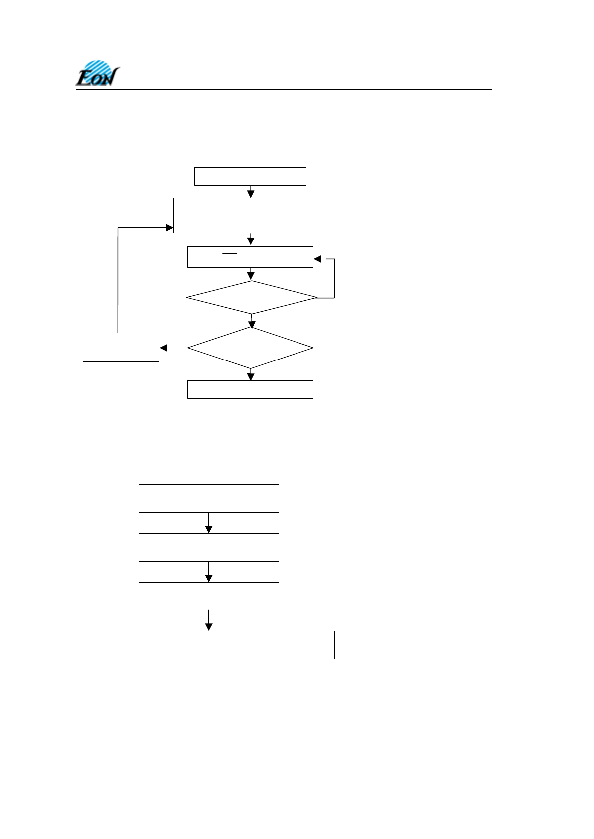
Flowchart 1. Embedded Program
START
Write Program
Command Sequence
(shown below)
Data Poll Device
Last
Address?
Programming Done
Increment
Address
No
Yes
Verify Data?
Flowchart 2. Embedded Program Command Sequence
See the Command Definitions section for more information.
2AAH / 55H
555H / AAH
555H / A0H
PROGRAM ADDRESS / PROGRAM DATA
Page 17
4800 Great America Parkway, Suite 202 Tel: 408-235-8680
Santa Clara, CA 95054 Fax: 408-235-8685
17
EN29F080
Rev. C, Issue Date: 2001/ 07/05
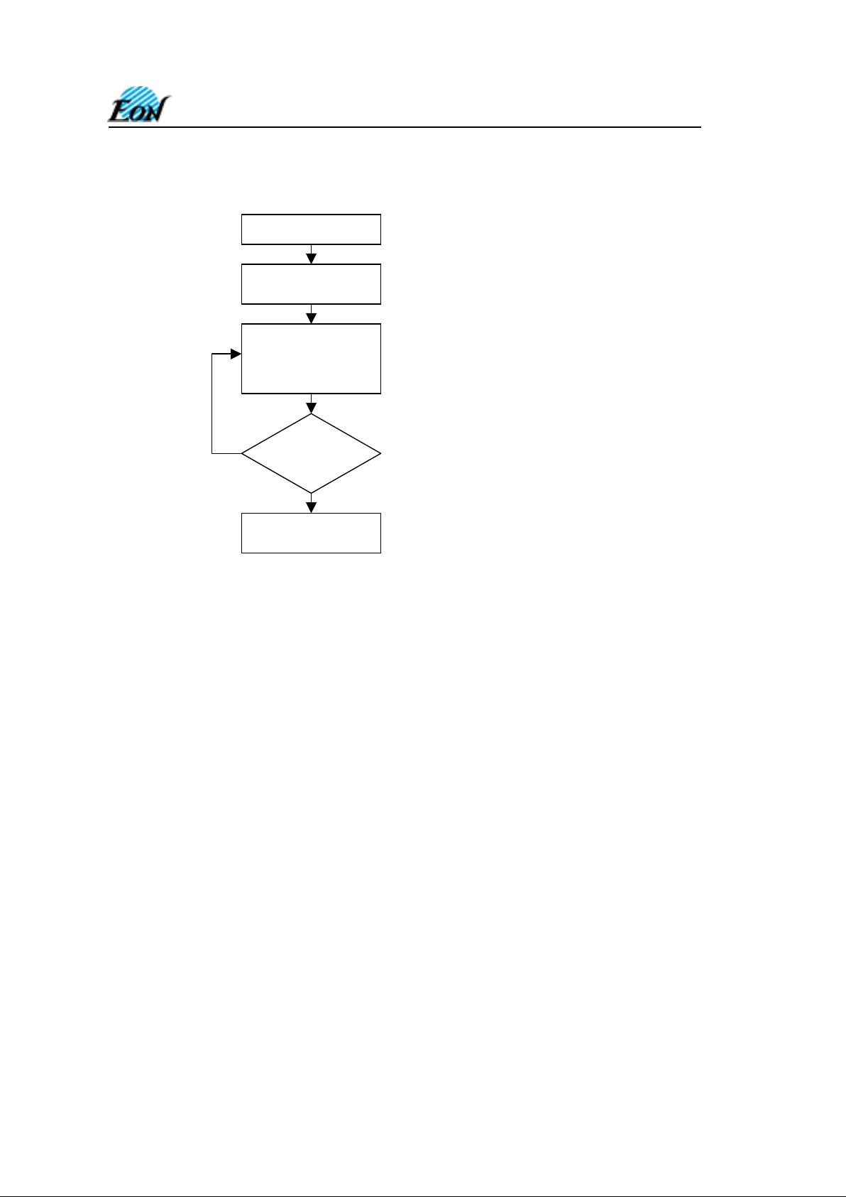
Flowchart 3. Embedded Erase
START
Write Erase
Command Sequence
Data Poll from
System or Toggle Bit
successfully
completed
Erase Done
Data =FFh?
Yes
No
Page 18
4800 Great America Parkway, Suite 202 Tel: 408-235-8680
Santa Clara, CA 95054 Fax: 408-235-8685
18
EN29F080
Rev. C, Issue Date: 2001/ 07/05
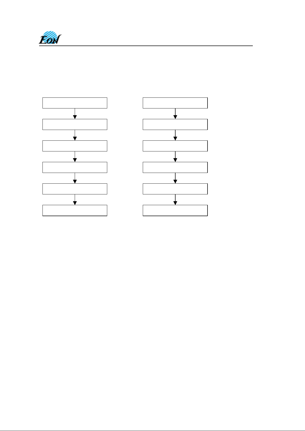
Flowchart 4. Embedded Erase Command Sequence
See the Command Definitions section for more information.
Chip Erase Sector Erase
2AAH/55H
555H/AAH
555H/80H
2AAH/55H
555H/AAH
555H/10H
555H/AAH
2AAH/55H
555H/80H
555H/AAH
2AAH/55H
Sector Address/30H
Page 19
4800 Great America Parkway, Suite 202 Tel: 408-235-8680
Santa Clara, CA 95054 Fax: 408-235-8685
19
EN29F080
Rev. C, Issue Date: 2001/ 07/05
Flowchart 5. DATAPolling
Algorithm
Flowchart 6. Toggle Bit Algorithm
No
Yes
DQ6 = T ogg le?
DQ5 = 1?
DQ6 = T ogg le?
No
No
Yes
Yes
Read Data
Start
Read Data
Fail Pass
No
No
DQ7 = Data?
DQ5 = 1?
DQ7 = Data?
Yes
Yes
No
Yes
Read Data
Start
Read Data
Fail Pass
Page 20
4800 Great America Parkway, Suite 202 Tel: 408-235-8680
Santa Clara, CA 95054 Fax: 408-235-8685
20
EN29F080
Rev. C, Issue Date: 2001/ 07/05
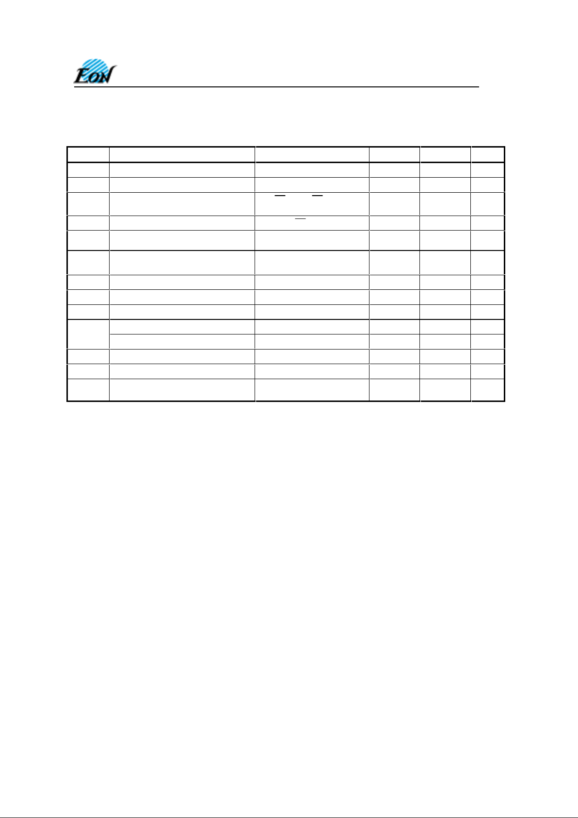
Table 7. DC Characteristics
(Ta = 0°C to 70°C or - 40°C to 85°C; VCC = 5.0V ± 10%)
Notes:
(1) RESET# pin input buffer is always enabled so that it draws power if not at full CMOS supply voltages
Symbol Parameter Test Conditions Min Max Unit
ILI
Input Leakage Current
0V≤ VIN ≤ Vcc
±5 µA
ILO
Output Leakage Current
0V≤ V
OUT
≤ Vcc
±5 µA
I
CC1
Supply Current (read) TTL Byte
CE = VIL; OE = VIH;
f = 6MHz
30 mA
I
CC2
Supply Current (Standby) TTL
CE = V
IH
1.0 mA
I
CC3
Supply Current (Standby) CMOS
(1)
RESET# = CE# =
Vcc ± 0.2V
5.0 µA
I
CC4
Supply Current (Program or Erase)
Byte program, Sector or
Chip Erase in progress
30
mA
VIL
Input Low Voltage -0.5 0.8 V
VIH
Input High Voltage 2 Vcc ± 0.5 V
VOL
Output Low Voltage
IOL = 2 mA
0.45 V
Output High Voltage TTL
IOH = -2.5 mA
2.4 V
VOH
Output High Voltage CMOS
IOH = -100 µA
Vcc - 0.4V V
VID
A9 Voltage (Electronic Signature) 10.5 11.5 V
I
LIT
A9 Current (Electronic Signature) A9 = VID 100 µA
V
LKO
Supply voltage (Erase and
Program lock-out)
3.2 4.2 V
Page 21
4800 Great America Parkway, Suite 202 Tel: 408-235-8680
Santa Clara, CA 95054 Fax: 408-235-8685
21
EN29F080
Rev. C, Issue Date: 2001/ 07/05
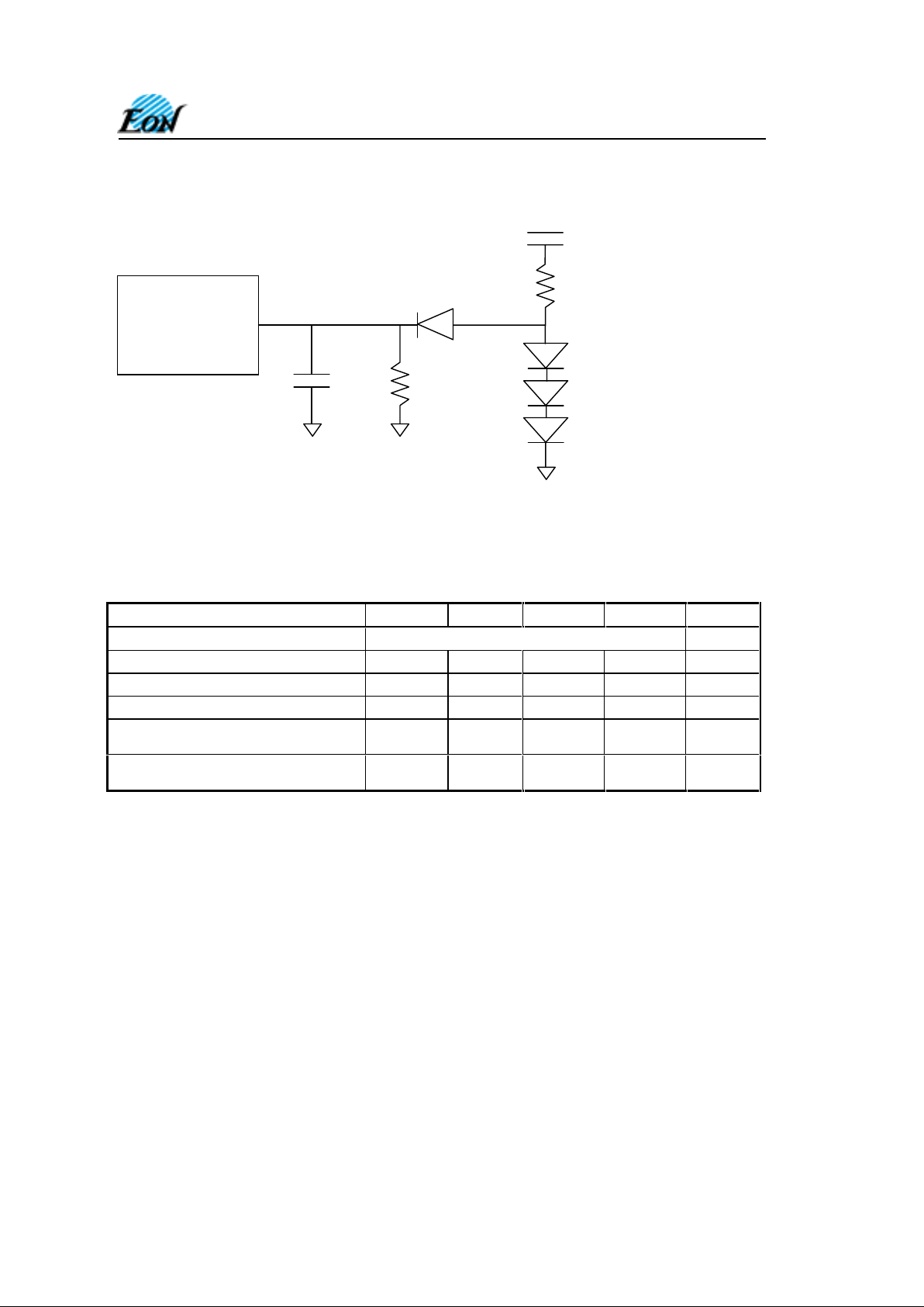
Test Conditions
Test Specifications
Test Conditions -45 -55 -70 -90 Unit
Output Load 1 TTL Gate
Output Load Capacitance, CL 30 30 100 100 pF
Input Rise and Fall times 5 5 20 20 ns
Input Pulse Levels 0.0-0.3 0.0-0.3 0.45-2.4 0.45-2.4 V
Input timing measurement
reference levels
1.5 1.5 0.8, 2.0 0.8, 2.0 V
Output timing measurement
reference levels
1.5 1.5 0.8, 2.0 0.8, 2.0 V
Device Under Test
C
L
6.2 kΩ
2.7 k
Ω
5.0 V
Note: Diodes are IN3064 or equivalent
Page 22
4800 Great America Parkway, Suite 202 Tel: 408-235-8680
Santa Clara, CA 95054 Fax: 408-235-8685
22
EN29F080
Rev. C, Issue Date: 2001/ 07/05
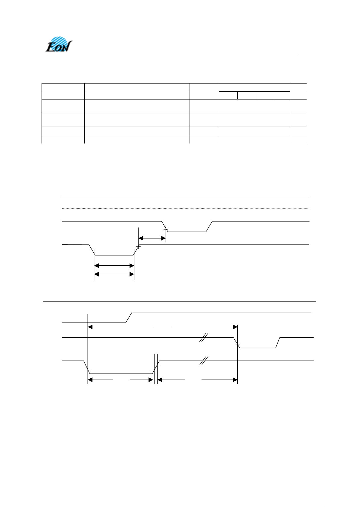
AC CHARACTERISTICS
Hardware Reset (Reset#)
Speed options
Parameter
Std
Description
Test
Setup
-45 -55 -70 -90
Unit
t
READY
Reset# Pin Low to Read or Write
Embedded Algorithms
Max 20
µ
s
t
READY
Reset# Pin Low to Read or Write
Non Embedded Algorithms
Max 500 ns
tRP Reset# Pulse Width Min 500 ns
tRH Reset# High Time Before Read Min 50 ns
Reset# Timings
tRH
t
RP
t
READY
0 V
RY/BY#
CE#
OE#
RESET#
Reset Timings NOT During Automatic Algorithms
t
READY
t
RH
tRP
RY/BY#
CE#
OE#
RESET#
Reset Timings During Automatic Algorithms
Page 23
4800 Great America Parkway, Suite 202 Tel: 408-235-8680
Santa Clara, CA 95054 Fax: 408-235-8685
23
EN29F080
Rev. C, Issue Date: 2001/ 07/05
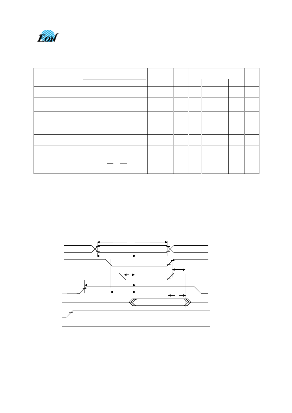
Table 8. AC CHARACTERISTICS
Read-only Operations Characteristics
Parameter
Symbols
Speed Options
JEDEC Standard
Description
Test
Setup
-45 -55 -70 -90 Unit
t
AVAV
t
RC
Read Cycle Time
Min 45 55 70 90 ns
t
AVQV
t
ACC
Address to Output Delay
CE
= V
IL
OE
= VIL
Max 45 55 70 90 ns
t
ELQV
t
CE
Chip Enable To Output Delay
OE
= VIL
Max 45 55 70 90 ns
t
GLQV
t
OE
Output Enable to Output Delay
Max 25 30 30 35 ns
t
EHQZ
t
DF
Chip Enable to Output High Z
Max 20 20 20 20 ns
t
GHQZ
t
DF
Output Enable to Output High Z
Max 20 20 20 20 ns
t
AXQX
t
OH
Output Hold Time from
Addresses,
CE
or OE,
whichever occurs first
Min 0 0 0 0 ns
Notes:
For - 50 Vcc = 5.0V ± 5%
Output Load : 1 TTL gate and 30pF
Input Rise and Fall Times: 5ns
Input Rise Levels: 0.0 V to 3.0 V
Timing Measurement Referenc e Level , Input and Output: 1.5 V
For all others: Vcc = 5.0V ± 10%
Output Load: 1 TTL gate and 100 pF
Input Rise and Fall Times: 20 ns
Input Pulse Levels: 0.45 V to 2.4 V
Timing Measurement Referenc e Level , Input and Output: 0.8 V and 2.0 V
Figure 5. AC Waveforms for READ Operations
Addresses
CE#
OE#
WE#
Outputs
Reset#
RY/BY#
0V
Output Valid
tRC
t
ACC
tOE
tCE
t
OEH
t
OH
t
DF
HIGH Z
Addresses Stable
Page 24
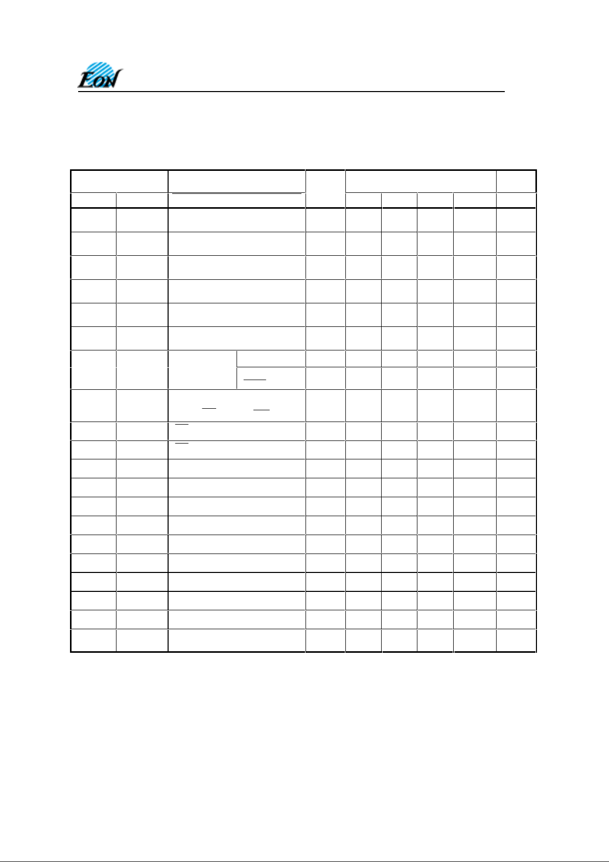
4800 Great America Parkway, Suite 202 Tel: 408-235-8680
Santa Clara, CA 95054 Fax: 408-235-8685
24
EN29F080
Rev. C, Issue Date: 2001/ 07/05
Table 9. AC CHARACTERISTICS
Write (Erase/Program) Operations
Parameter
Symbols
Speed Options
JEDEC Standard
Description
-45 -55 -70 -90 Unit
t
AVAV
t
WC
Write Cycle Time
Min 45 55 70 90 ns
t
AVWL
t
AS
Address Setup Time
Min 0 0 0 0 ns
t
WLAX
t
AH
Address Hold Time
Min 35 45 45 45 ns
t
DVWH
t
DS
Data Setup Time
Min 20 25 30 45 ns
t
WHDX
t
DH
Data Hold Time
Min 0 0 0 0 ns
t
OES
Output Enable Setup Time
Min 0 0 0 0 ns
Read
MIn 0 0 0 0 ns
t
OEH
Output Enable
Hold Time
Toggle and
DATA
Polling
Min 10 10 10 10 ns
t
GHWL
t
GHWL
Read Recovery Time before
Write (
OE
High to WE Low)
Min
0 0 0 0 ns
t
ELWL
t
CS
CE
SetupTime
Min
0 0 0 0 ns
t
WHEH
t
CH
CE
Hold Time
Min
0 0 0 0 ns
t
WLWH
t
WP
Write Pulse Width
Min
25 30 35 45 ns
t
WHDL
t
WPH
Write Pulse Width High
Min
20 20 20 20 ns
t
WHWH1
t
WHWH1
Programming Operation
Typ
7 7 7 7 µs
Max
200 200 200 200 µs
t
WHWH2
t
WHWH2
Sector Erase Operation
Typ
0.3 0.3 0.3 0.3 s
Max
5 5 5 5 s
t
WHWH3
t
WHWH3
Chip Erase Operation
Typ
3 3 3 3 s
Max
35 35 35 35 s
t
VCS
Vcc Setup Time
Min
50 50 50 50 µs
t
VIDR
Rise Time to V
ID
Min
500 500 500 500 ns
Page 25
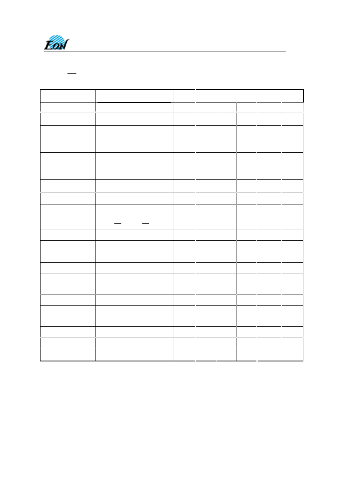
4800 Great America Parkway, Suite 202 Tel: 408-235-8680
Santa Clara, CA 95054 Fax: 408-235-8685
25
EN29F080
Rev. C, Issue Date: 2001/ 07/05
Table 10. AC CHARACTERISTICS
Write (Erase/Program) Operations
Alternate CE Controlled Writes
Parameter
Symbols
Speed Options
JEDEC Standard
Description
-45 -55 -70 -90 Unit
t
AVAV
t
WC
Write Cycle Time
Min 45 55 70 90 ns
t
AVEL
t
AS
Address Setup Time
Min 0 0 0 0 ns
t
ELAX
t
AH
Address Hold Time
Min 35 45 45 45 ns
t
DVEH
t
DS
Data Setup Time
Min 20 25 30 45 ns
t
EHDX
t
DH
Data Hold Time
Min 0 0 0 0 ns
t
OES
Output Enable Setup Time
Min 0 0 0 0 ns
t
OEH
Output Enable Read
0 0 0 0 0 ns
Hold Time Toggle and
Data Polling
10 10 10 10 10 ns
t
GHEL
t
GHEL
Read Recovery Time before
Write (
OE
High to CE Low)
Min
0 0 0 0 ns
t
WLEL
t
WS
WE
SetupTime
Min
0 0 0 0 ns
t
EHWH
t
WH
WE
Hold Time
Min
0 0 0 0 ns
t
ELEH
t
CP
Write Pulse Width
Min
25 30 35 45 ns
t
EHEL
t
CPH
Write Pulse Width High
Min
20 20 20 20 ns
t
WHWH1
t
WHWH1
Programming Operation
Typ
7 7 7 7 µs
Max
200 200 200 200 µs
t
WHWH2
t
WHWH2
Sector Erase Operation
Typ
0.3 0.3 0.3 0.3 s
Max
5 5 5 5 s
t
WHWH3
t
WHWH3
Chip Erase Operation
Typ
3 3 3 3 s
Max
35 35 35 35 s
t
VCS
Vcc Setup Time
Min
50 50 50 50 µs
t
VIDR
Rise Time to V
ID
Min
500 500 500 500 ns
Page 26
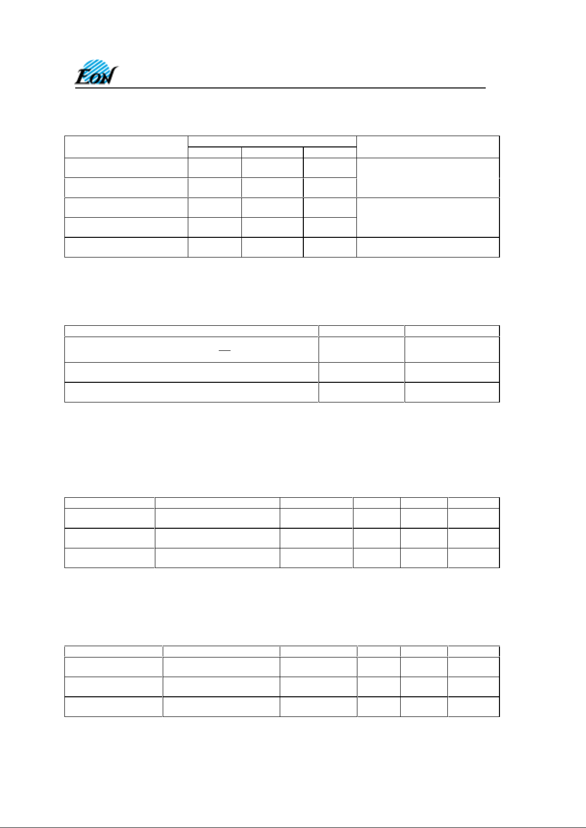
4800 Great America Parkway, Suite 202 Tel: 408-235-8680
Santa Clara, CA 95054 Fax: 408-235-8685
26
EN29F080
Rev. C, Issue Date: 2001/ 07/05
Table 11. ERASE AND PROGRAMMING PERFORMANCE
Limits
Parameter
Typ Max Unit
Comments
Sector Erase Time 0.3 5 sec
Chip Erase Time 3 35 sec
Excludes 00H programming prior
to erasure
Byte Programming Time 7 200 µs
Chip Programming Time 2 5 sec
Excludes system level overhead
Erase/Program Endurance 100K cycles
Minimum 100K cycles guaranteed
Table 12. LATCH UP CHARACTERISTICS
Parameter Description Min Max
Input voltage with respect to Vss on all pins except I/O pins
(including A9 and OE)
-1.0 V 12.0 V
Input voltage with respect to Vss on all I/O Pins -1.0 V Vcc + 1.0 V
Vcc Current -100 mA 100 mA
Note : These are latch up characteristics and the device should never be put under
these conditions. Refer to Absolute Maximum ratings for the actual operating limits.
Table 13. 32-PIN PLCC PIN CAPACITANCE @ 25°C, 1.0MHz
Parameter Symbol Parameter Description Test Setup Typ Max Unit
CIN
Input Capacitance
VIN = 0
4 6 pF
C
OUT
Output Capacitance
V
OUT
= 0
8 12 pF
C
IN2
Control Pin Capacitance
VIN = 0
8 12 pF
Table 14. 32-PIN TSOP PIN CAPACITANCE @ 25°C, 1.0MHz
Parameter Symbol Parameter Description Test Setup Typ Max Unit
CIN
Input Capacitance
VIN = 0
6 7.5 pF
C
OUT
Output Capacitance
V
OUT
= 0
8.5 12 pF
C
IN2
Control Pin Capacitance
VIN = 0
7.5 9 pF
Page 27

4800 Great America Parkway, Suite 202 Tel: 408-235-8680
Santa Clara, CA 95054 Fax: 408-235-8685
27
EN29F080
Rev. C, Issue Date: 2001/ 07/05
Table 15. DATA RETENTION
Parameter Description Test Conditions Min Unit
150°C 10 Years
Minimum Pattern Data Retention Time
125°C 20 Years
Page 28
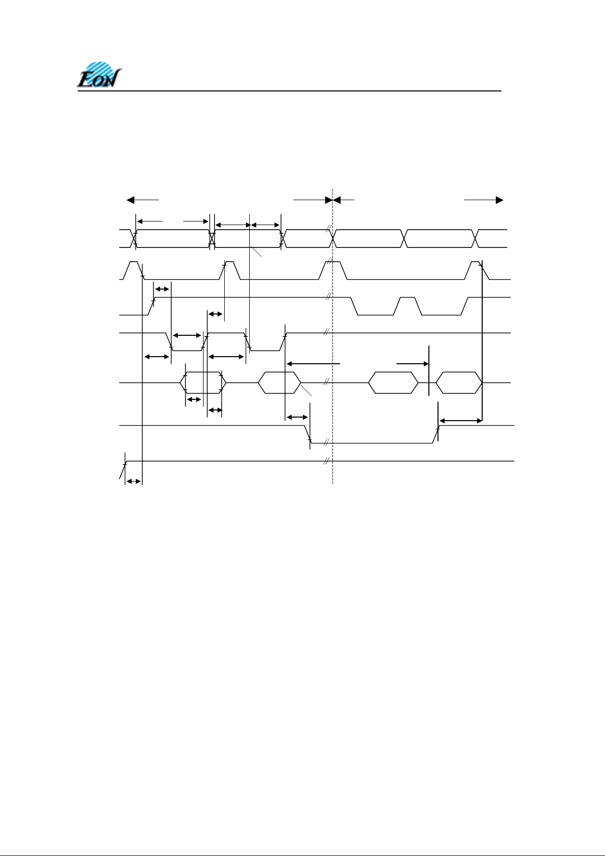
4800 Great America Parkway, Suite 202 Tel: 408-235-8680
Santa Clara, CA 95054 Fax: 408-235-8685
28
EN29F080
Rev. C, Issue Date: 2001/ 07/05
SWITCHING WAVEFORMS
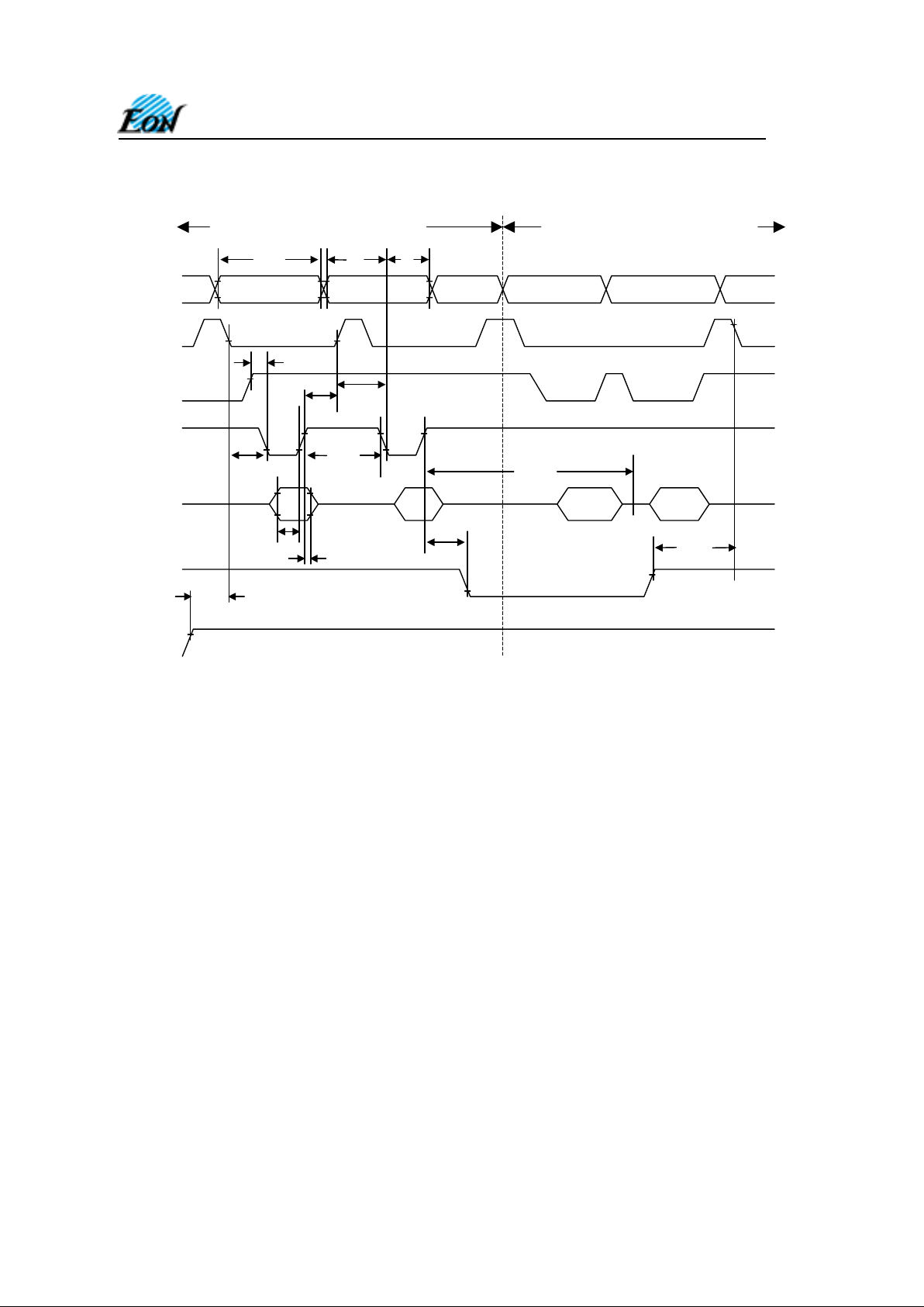
Figure 6. AC Waveforms for Chip/Sector Erase Operations Timings
Notes:
1. SA=Sector Address (for sector erase), VA=Valid Address for reading status, D
out
=true data at read address.
2. V
cc
shown only to illustrate t
vcs
measurement references. It cannot occur as shown during a valid command
sequence.
tDH
t
DS
t
BUSY
t
WPH
t
CH
t
WP
t
CS
t
VCS
t
RB
t
WC
t
AS
tAH
t
GHWL
t
WHWH2
or t
WHWH3
0x2AA SA VA VA
0x55 0x30 Status D
OUT
Addresses
CE#
OE#
WE#
Data
RY/BY#
V
CC
0x555 for chip
erase
0x555 for chip
erase
Erase Command Sequence (last 2 cycles) Read Status Data (last two cycles)
Page 29
4800 Great America Parkway, Suite 202 Tel: 408-235-8680
Santa Clara, CA 95054 Fax: 408-235-8685
29
EN29F080
Rev. C, Issue Date: 2001/ 07/05
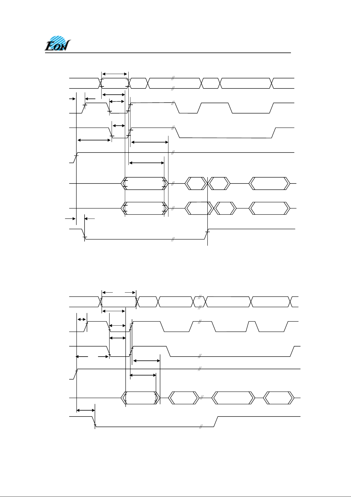
Figure 7. Program Operation Timings
Notes:
1. PA=Program Address, PD=Program Data, D
OUT
is the true data at the program address.
2. V
CC
shown in order to illustrate t
VCS
measurement references. It cannot occur as shown during a valid
command sequence.
t
VCS
t
DH
t
RB
t
WHWH1
t
BUSY
t
DS
t
CS
t
WPH
t
CH
t
WP
t
GHWL
t
WC
t
AS
tAH
0x555 PA PA PA
PD Status D
OUT
OxA0
Addresses
CE#
OE#
WE#
Data
RY/BY#
V
CC
Program Command Sequence (last 2 cycles) Program Command Sequence (last 2 cycles)
Page 30
4800 Great America Parkway, Suite 202 Tel: 408-235-8680
Santa Clara, CA 95054 Fax: 408-235-8685
30
EN29F080
Rev. C, Issue Date: 2001/ 07/05
Figure 8. AC Waveforms for /DATA Polling During Embedded Algorithm Operations
Notes:
1. VA=Valid Address for reading Data# Polling status data
2. This diagram shows the first status cycle after the command sequence, the last status read cycle and the array data read cycle.
Figure 9. AC Waveforms for Toggle Bit During Embedded Algorithm Operations
t
OEH
t
DF
t
OH
t
BUSY
t
OE
Complement
Status Data
Complement
True
True
Status
Data
Valid Data
Valid Data
t
CE
t
ACC
t
CH
t
RC
VA
VA
VA
Addresses
CE#
OE#
WE#
DQ[7]
DQ[6:0]
RY/BY#
tRC
t
ACC
t
CE
t
OE
t
OEH
t
CH
t
DF
t
OH
t
BUSY
VA VA VA VA
Valid Status
Valid Status
Valid Status
Valid Data
(first read) (second read) (stops toggling)
Addresses
CE#
OE#
WE#
DQ6, DQ2
RY/BY#
Page 31
4800 Great America Parkway, Suite 202 Tel: 408-235-8680
Santa Clara, CA 95054 Fax: 408-235-8685
31
EN29F080
Rev. C, Issue Date: 2001/ 07/05
AC CHARACTERISTICS
DQ2 vs. DQ6
Temporary Sector Unprotect
Speed Option
Parameter
Std
Description
-45 -55 -70 -90
Unit
t
VIDR
V
ID
Rise and Fall Time Min 500 Ns
t
RSP
RESET# Setup Time for Temporary
Sector Unprotect
Min 4 µs
Temporary Sector Group Unprotect Timing Diagram
RESET#
0 or 5 V
t
VIDR
t
VIDR
t
RSP
VID
0 or 5V
CE#
WE#
RY/BY#
WE#
DQ6
DQ2
Enter
Embedded
Erase
Erase
Suspend
Enter Erase
Suspend
Program
Erase
Resume
Erase Enter
Suspend
Read
Enter
Suspend
Program
Erase
Erase
Complete
Erase
Suspend
Read
Page 32
4800 Great America Parkway, Suite 202 Tel: 408-235-8680
Santa Clara, CA 95054 Fax: 408-235-8685
32
EN29F080
Rev. C, Issue Date: 2001/ 07/05
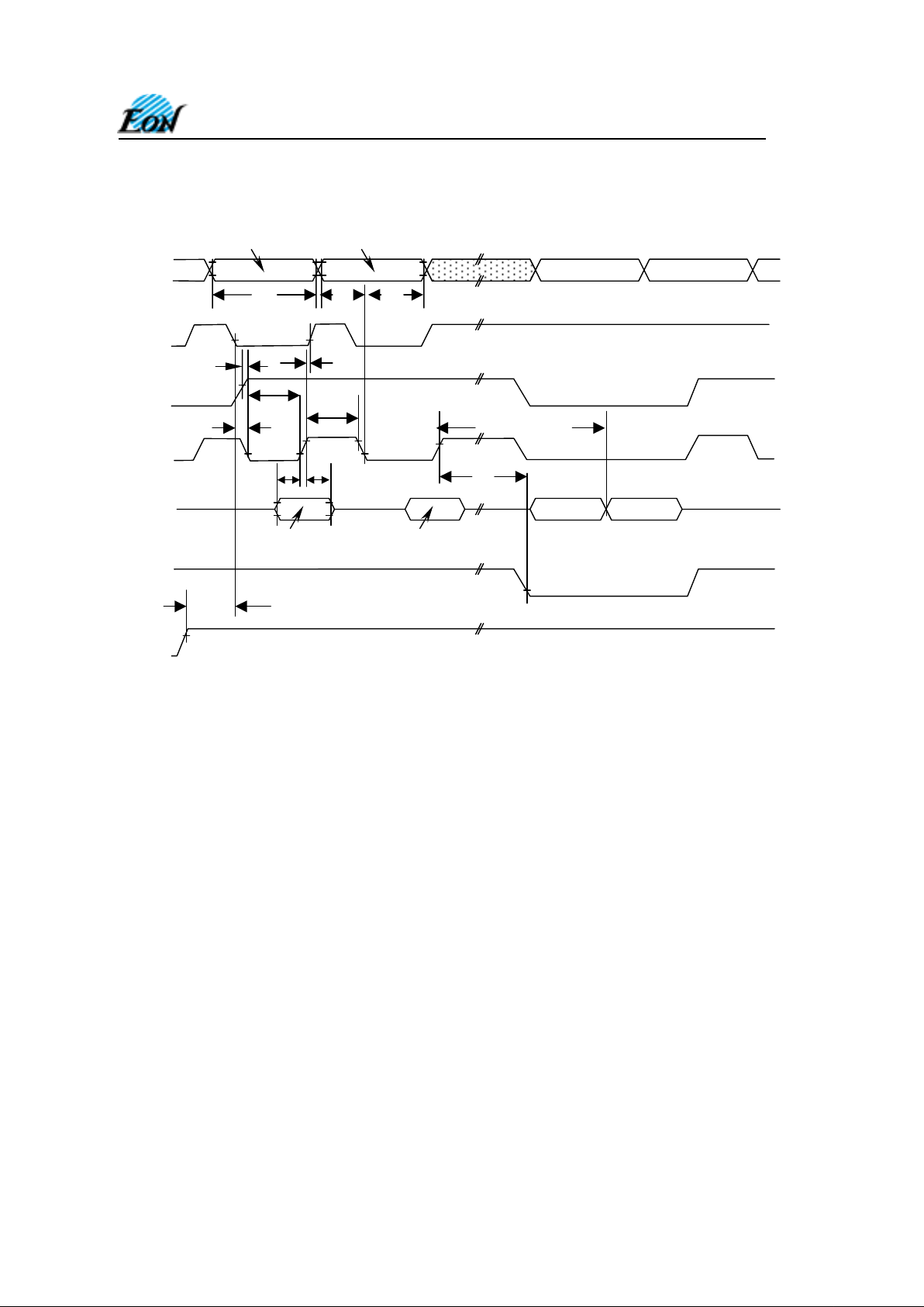
Figure 10. Alternate CE# Controlled Write Operation Timings
Notes:
PA = address of the memory location to be programmed.
PD = data to be programmed at byte address.
VA = Valid Address for reading program or erase status
D
out
= array data read at VA
Shown above are the last two cycles of the program or erase command sequence and the last staus read cycle
Reset# shown to illustrate t
RH
measurement references. It cannot occur as shown during a valid command
sequence.
tWC
tRH
t
AS
tAH
tWH
t
GHEL
t
CPH
tCP
tWS
tDH tDS
t
BUSY
t
CWHWH1
/ t
CWHWH2
/ t
CWHWH3
Status D
OUT
0xA0 for Program
0x55 for Erase
PD for Program
0x30 for Sector Erase
0x10 for Chip Erase
VA
Addresses
WE#
OE#
CE#
Data
RY/BY#
Reset#
PA for Program
SA for Sector Erase
0x555 for Chip Erase
0x555 for Program
0x2AA for Erase
Page 33
4800 Great America Parkway, Suite 202 Tel: 408-235-8680
Santa Clara, CA 95054 Fax: 408-235-8685
33
EN29F080
Rev. C, Issue Date: 2001/ 07/05
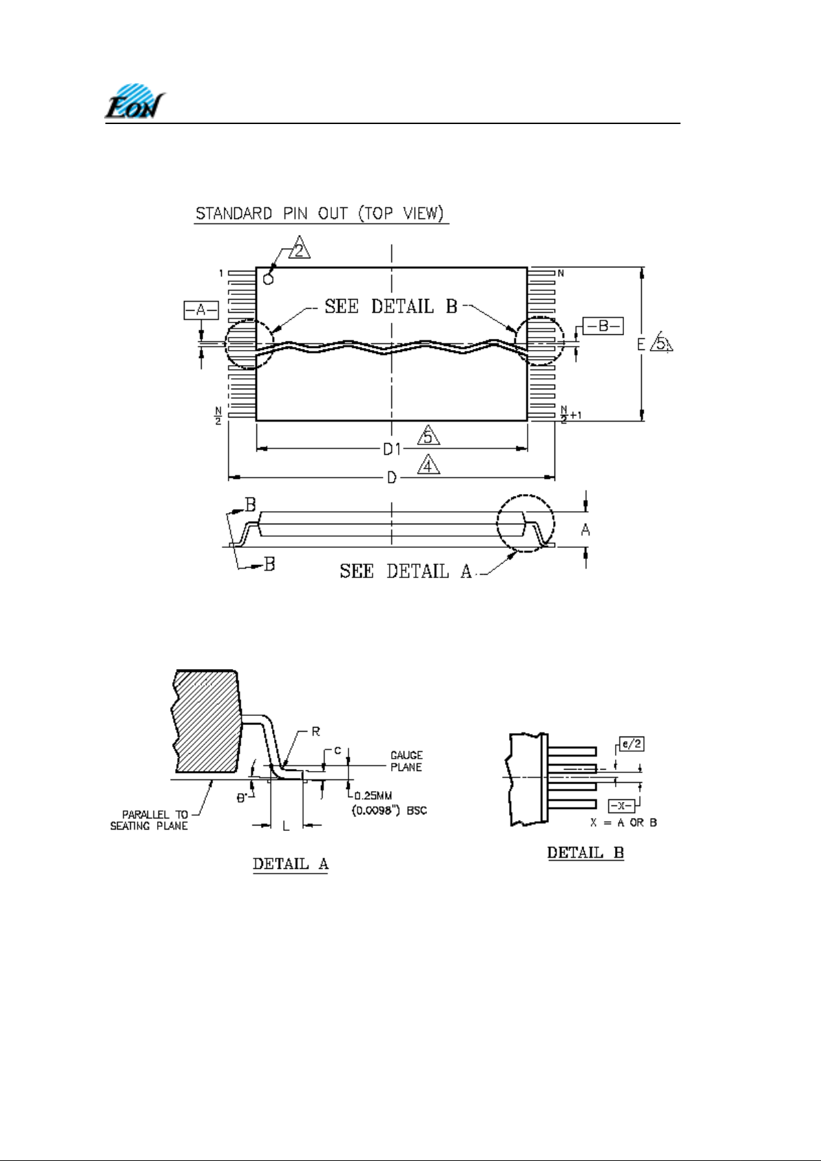
FIGURE 4. TSOP
Page 34
4800 Great America Parkway, Suite 202 Tel: 408-235-8680
Santa Clara, CA 95054 Fax: 408-235-8685
34
EN29F080
Rev. C, Issue Date: 2001/ 07/05
Page 35
4800 Great America Parkway, Suite 202 Tel: 408-235-8680
Santa Clara, CA 95054 Fax: 408-235-8685
35
EN29F080
Rev. C, Issue Date: 2001/ 07/05
ABSOLUTE MAXIMUM RATINGS
Parameter Value Unit
Storage Temperature -65 to +125
°
C
Plastic Packages -65 to +125
°
C
Ambient Temperature
With Power Applied
-55 to +125
°
C
Output Short Circuit Current1 200 mA
A9, OE#, Reset# 2 -0.5 to +11.5 V
All other pins 3 -0.5 to Vcc+0.5 V
Voltage with
Respect to Ground
Vcc -0.5 to +7.0 V
Notes:
1. No more than one output shorted at a time. Duration of the short circuit should not be greater than one second.
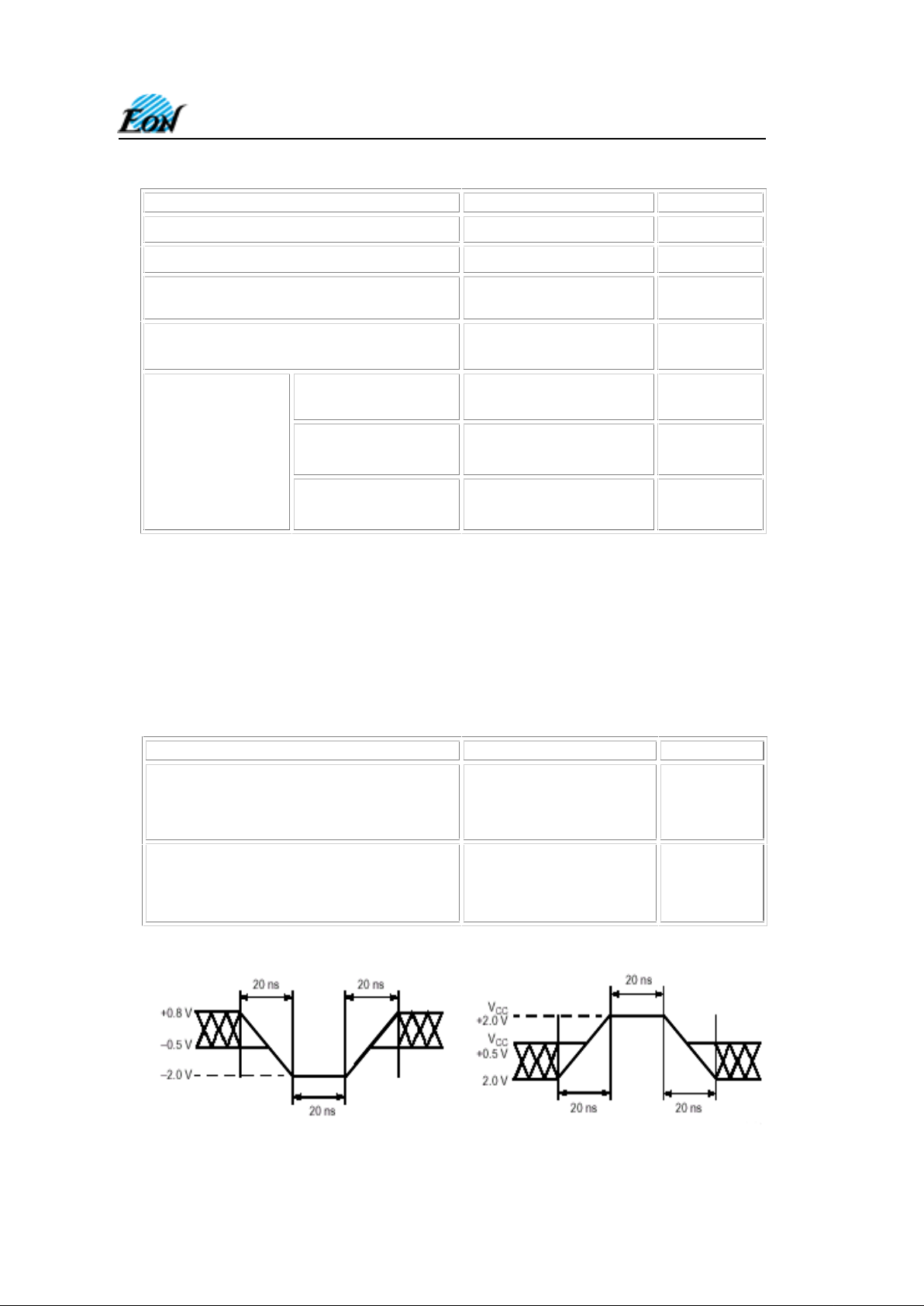
2. Minimum DC input voltage on A9, OE#, RESET# pins is –0.5V. During voltage transitions, A9, OE#, RESET# pins may
undershoot V
ss
to –1.0V for periods of up to 50ns and to –2.0V for periods of up to 20ns. See figure below. Maximum DC
input voltage on A9, OE#, and RESET# is 11.5V which may overshoot to 12.5V for periods up to 20ns.
3. Minimum DC voltage on input or I/O pins is –0.5 V. During voltage transitions, inputs may undershoot Vss to –1.0V for periods
of up to 50ns and to –2.0 V for periods of up to 20ns. See figure below. Maximum DC voltage on output and I/O pins is V
cc
+
0.5 V. During voltage transitions, outputs may overshoot to V
cc
+ 2.0 V for periods up to 20ns. See figure below.
4. Stresses above the values so mentioned above may cause permanent damage to the device. These values are for a stress
rating only and do not imply that the device should be operated at conditions up to or above these values. Exposure of the
device to the maximum rating values for extended periods of time may adversely affect the device reliability.
RECOMMENDED OPERATING RANGES1
Parameter Value Unit
Ambient Operating Temperature
Commercial Devices
Industrial Devices
0 to 70
-40 to 85
°
C
Operating Supply Voltage
Vcc for
±
5% devices
Vcc for
±
10% devices
4.75 to 5.25
4.5 to 5.5
V
1. Recommended Operating Ranges define those limits between which the functionality of the device is guaranteed.
Maximum Negative Overshoot Waveform Maximum Positive Overshoot Waveform
Page 36

4800 Great America Parkway, Suite 202 Tel: 408-235-8680
Santa Clara, CA 95054 Fax: 408-235-8685
36
EN29F080
Rev. C, Issue Date: 2001/ 07/05
ORDERING INFORMATION
EN29F080 50 T I
TEMPERATURE RANGE
(Blank) = Commercial (0°C to +70°C)
I = Industrial (-40°C to +85°C)
PACKAGE
T = 40-pin
S = Small Outline Package
SPEED
45 = 45ns
50 = 50ns
70 = 70ns
90 = 90ns
BASE PART NUMBER
EN = EON Silicon Devices
29F = FLASH, 5V Read Program Erase
080 = 8 Megabit (1024K x 8)
Page 37

4800 Great America Parkway, Suite 202 Tel: 408-235-8680
Santa Clara, CA 95054 Fax: 408-235-8685
37
EN29F080
Rev. C, Issue Date: 2001/ 07/05
Revisions List
A:
Preliminary
B (2001.07.03):
Table 7. Icc3 is with RESET# pin at full CMOS levels
Pg. 15 Logical Inhibit section now says that if
CE
, WE, and OE are all logical zero
(not recommended usage), it will be considered a write.
VID is everywhere changed to be VID =11.5 ± 0.5V
C (2001.07.05):
“block” changed to “sector”
Deleted Sector Un/Protect flow charts (we have a supplement for that)
VID is everywhere changed to be VID =11.0 ± 0.5V
LACTHUP >= 200mA line removed from first page
Chip erase and Sector Erase command descriptions modified.
DQ7,DQ5,DQ3 statu s polling descriptions modified.
Table 12 Latchup characteristics modified
Changed P/E endurance to 100K everywhere
 Loading...