

Datasheet EN29F002T90TI, EN29F002T90JI, EN29F002T70TI, EN29F002T70JI, EN29F002T55TI Datasheet (EON)
...Page 1

4800 Great America Parkway, Suite 202 Tel: 408-235-8680
Santa Clara, CA 95054 Fax: 408-235-8685
1
EN29F002 / EN29F002N
Rev. C, Issue Date: 2001/ 07/05
FEATURES
•
5.0V ± 10% for both read/write operation
•
Read Access Time
- 45ns, 55ns, 70ns, and 90ns
•
Fast Read Access Time
- 70ns with C
load
= 100pF
- 45ns, 55ns with C
load
= 30pF
•
Sector Architecture:
One 16K byte Boot Sector, Two 8K byte
Parameter Sectors, one 32K byte and
three 64K byte main Sectors
•
Boot Block Top/Bottom Programming
Architecture
•
High performance program/erase speed
- Byte program time: 10µs typical
- Sector erase time: 500ms typical
- Chip erase time: 3.5s typical
•
Low Standby Current
- 1µA CMOS standby current-typical
- 1mA TTL standby current
•
Low Power Active Current
- 30mA active read current
- 30mA program / erase current
•
JEDEC Standard program and erase
commands
•
JEDEC standard
DATA
polling and toggle
bits feature
•
Hardware
RESET
Pin (n/a for EN29F002N)
•
Single Sector and Chip Erase
•
Sector Protection / Temporary Sector
Unprotect (
RESET
= VID)
•
Sector Unprotect Mode
•
Embedded Erase and Program Algorithms
•
Erase Suspend / Resume modes:
Read and program another sector during
Erase Suspend Mode
•
0.4 µm double-metal double-poly
triple-well CMOS Flash Technology
•
Low Vcc write inhibit < 3.2V
•
100K endurance cycle
•
Package Options
- 32-pin PDIP
- 32-pin PLCC
- 32-pin TSOP (Type 1)
•
Commercial and Industrial Temperature
Ranges
GENERAL DESCRIPTION
The EN29F002 / EN29F002N is a 2-Megabit, electrically erasable, read/write non-volatile flash memory.
Organized into 256K words with 8 bits per word, the 2M of memory is arranged in seven sectors (with
top/bottom configuration), including one 16K Byte Boot Sector, two 8K Byte Parameter sectors, and four main
sectors (one 32K Byte and three 64K Byte). Any byte can be programmed typically at 10µs. The EN29F002 /
EN29F002N features 5.0V voltage read and write operation. The access times are as fast as 45ns to eliminate
the need for WAIT states in high-performance microprocessor systems.
The EN29F002 / EN29F002N has separate Output Enable (
OE
), Chip Enable (CE), and Write
Enable (
WE
) controls which eliminate bus contention issues. This device is designed to allow
either single sector or full chip erase operation, where each sector can be individually protected
against program/erase operations or temporarily unprotected to erase or program. The device can
sustain a minimum of 100K program/erase cycles on each sector.
EN29F002 / EN29F002N
2 Megabit (256K x 8-bit) Flash Memory
Page 2

4800 Great America Parkway, Suite 202 Tel: 408-235-8680
Santa Clara, CA 95054 Fax: 408-235-8685
2
EN29F002 / EN29F002N
Rev. C, Issue Date: 2001/ 07/05
TABLE 1. PIN DESCRIPTION FIGURE 1. LOGIC DIAGRAM
Pin Name Function
A0-A17 Addresses
DQ0-DQ7 Data Input/Outputs
CE
Chip Enable
OE
Output Enable
WE
Write Enable
RESET
(n/a for
EN29F002N)
Hardware Reset
Sector Unprotect
Vcc Supply Voltage
(5V ± 10% )
Vss Ground
TABLE 2. BLOCK ARCHITECTURE
TOP BOOT BLOCK BOTTOM BOOT BLOCK
SECTOR ADDRESSES
SIZE (Kbytes)
ADDRESSES
SIZE (Kbytes)
6 3C000h - 3FFFFh 16 30000h - 3FFFFh 64
5 3A000h - 3BFFFh 8 20000h - 2FFFFh 64
4 38000h - 39FFFh 8 10000h - 1FFFFh 64
3 30000h - 37FFFh 32 08000h - 0FFFFh 32
2 20000h - 2FFFFh 64 06000h - 07FFFh 8
1 10000h - 1FFFFh 64 04000h - 05FFFh 8
0 00000h - 0FFFFh 64 00000h - 03FFFh 16
EN29F002T/B
8
DQ0 - DQ7A0 - A17
18
Vcc
WE
CE
OE
RESET
Vss
NC on EN29F002N
Page 3

4800 Great America Parkway, Suite 202 Tel: 408-235-8680
Santa Clara, CA 95054 Fax: 408-235-8685
3
EN29F002 / EN29F002N
Rev. C, Issue Date: 2001/ 07/05
BLOCK DIAGRAM
RESET
WE
CE
OE
State
Control
Command
Register
Erase Voltage Generator
Input/Output Buffers
Program Voltage
Generator
Chip Enable
Output Enable
Logic
Data Latch
Y-Decoder
X-Decoder
Y-Gating
Cell Matrix
TimerVcc Detector
A0-A17
Vcc
Vss
DQ0-DQ7
Ad
d
r
e
s
s
L
a
t
c
h
Block Protect Switches
STB
STB
N/A on EN29F002N
Page 4

4800 Great America Parkway, Suite 202 Tel: 408-235-8680
Santa Clara, CA 95054 Fax: 408-235-8685
4
EN29F002 / EN29F002N
Rev. C, Issue Date: 2001/ 07/05
FIGURE 2. PDIP
FIGURE 3. TSOP
EN29F002
FIGURE 4. PLCC
PLCC Top View
A7
A6
A5
A4
A3
A2
A1
A0
DQ0
5
6
7
8
9
10
11
12
13
29
28
27
26
25
24
23
22
21
A14
A13
A8
A9
A11
OE
A10
CE
DQ7
4232
3131
30
14 16 18
15 17 19
20
DQ1 VSS DQ4
DQ2 DQ3 DQ5
DQ6
A12 A16 VCC
A15 VPP PGM
NC
PDIP Top View
VPP
A16
A15
A12
A7
A6
A5
A4
A3
A2
A1
A0
DQ0
DQ1
DQ2
VSS
VCC
PGM
NC
A14
A13
A8
A9
A11
OE
A10
CE
DQ7
DQ6
DQ5
DQ4
DQ3
1
2
3
4
5
6
7
8
9
10
11
12
13
14
15
16
32
31
30
29
28
27
26
25
24
23
22
21
20
19
18
17
A17
WE
RESET
WE
RESET
A15 RESET WE
A12 A16 V
CC
A17
N/A for EN29F002N
N/A for EN29F002N
RESET is not applicable for EN29F002N
Page 5
4800 Great America Parkway, Suite 202 Tel: 408-235-8680
Santa Clara, CA 95054 Fax: 408-235-8685
5
EN29F002 / EN29F002N
Rev. C, Issue Date: 2001/ 07/05
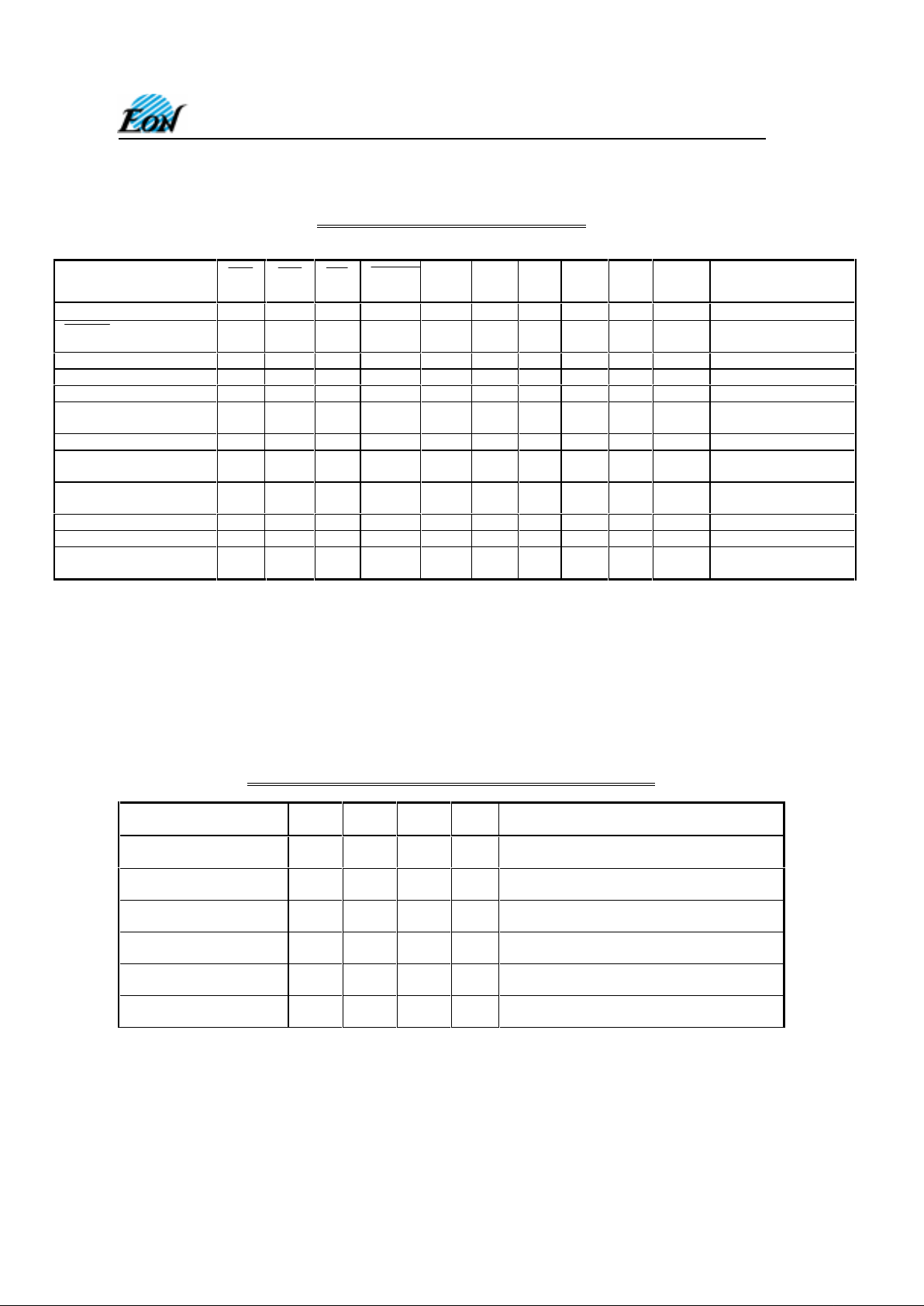
TABLE 3. OPERATING MODES
2M FLASH USER MODE TABLE
CE
WE OE
RESET
A9 A8 A6 A1 A0 Ax/y DQ(0-7)
USER MODE
RESET
(n/a for EN29F002N)
X X X L X X X X X X HI-Z
STANDBY H X X H X X X X X X HI-Z
READ L H L H A9 A8 A6 A1 A0 Ax/y DQ(0-7)
OUTPUT DISABLE L H H H A9 A8 A6 A1 A0 Ax/y HI-Z
READ
MANUFACTURER ID
L H L H VID L/H L L L X MANUFACTURER
ID
READ DEVICE ID L H L H VID L/H L L H X DEVICE ID(T/B)
VERIFY SECTOR
PROTECT
L H L H VID X L H L X CODE
ENABLE SECTOR
PROTECT
L L VID H VID X L X X X X
SECTOR UNPROTECT L L VID H VID X H H L X X
WRITE L L H H A9 A8 A6 A1 A0 Ax/y DIN(0-7)
TEMPORARY SECTOR
UNPROTECT
X X X VID X X X X X X X
NOTES:
1) L = V
IL
, H = VIH, VID = 11.0V ± 0.5V
2) X = Don’t care, either V
IH
or VIL
TABLE 4. DEVICE IDENTIFICTION
2M FLASH MANUFACTURER/DEVICE ID TABLE
A8 A6 A1 A0 DQ(7-0)
HEX
READ
MANUFACTURER ID
L L L L MANUFACTURER ID
7F
READ
MANUFACTURER ID
H L L L MANUFACTURER ID
1C
READ DEVICE ID
(Top Architecture)
L L L H DEVICE ID
7F
READ DEVICE ID
(Top Architecture)
H L L H DEVICE ID
92
READ DEVICE ID
(Bottom Architecture)
L L L H DEVICE ID
7F
READ DEVICE ID
(Bottom Architecture)
H L L H DEVICE ID
97
Page 6

4800 Great America Parkway, Suite 202 Tel: 408-235-8680
Santa Clara, CA 95054 Fax: 408-235-8685
6
EN29F002 / EN29F002N
Rev. C, Issue Date: 2001/ 07/05
USER MODE DEFINITIONS
Reset Mode
EN29F002 features a Reset mode that res ets the program and erase operation immediately to read
mode. If reset (
RESET
= L) is executed when program or erase operation were in progress, the
program or erase which was term inated should be repeated since data will be corrupted. This pin is
not available for EN29F002N.
Standby Mode
The EN29F002 / EN29F002N has a CMOS-com patible standby mode which reduces the
current to <
1µA (typical). It is placed in CMOS-com patible standby when
CE
and the
RESET
pins are at VCC ±
0.5 V (
CE
pin only, for EN29F002N). The device also has a T TL-c ompatible standby mode which
reduces the maxim um V
CC
current to < 1m A. It is placed in TTL-c ompatible standby when CE and
RESET
pins are at VIH. Another method of entering standby mode uses only the
RESET
pin (n/a for
EN29F002N). When
RESET
pin is at VSS ± 0.3V, the device enters CMOS- compatible standby with
current typically reduced to < 1 µA. W hen
RESET
pin is at VIL, the device enters TTL-c ompatible
standby with current reduced to < 1mA. When in standby modes, the outputs are in a highimpedance state independent of the
OE
input.
Read Mode
The EN29F002 / EN29F002N has two control functions which m ust be satisfied in order to obtain
data at the outputs. Chip Enable (
CE
) is the power control and should be used for device selection.
Output Enable (
OE
) is the output control and should be used to gate data to the output pins,
provided the device is selected. Read is s elected when both
CE
and OE pins are held at VIL with
the
WE
pin held at VIH. Address access time (t
ACC
) is equal to the delay from s table addresses to
valid output data. Assuming that addresses ar e stable, chip enable access tim e (t
CE
) is equal to the
delay from stable
CE
to valid data at output pins. Data is available at the outputs after output enable
access time (t
OE
) from the falling edge of OE, assuming the CE has been LOW and addresses
have been stable for at least t
ACC
- tOE.
Output Disable Mode
When the
CE
or OE pin is at a logic high level (VIH), the output from the EN29F002 / EN29F002N
is disabled. The output pins are placed in a high impedance state.
Auto Select Identification Mode
The manufac turer and device type can be identified by hardware or software operations. T his mode
allows applications or programming equipment automatically matching the device with its
corresponding interface characteristics.
To activate the Auto Select Identification mode, the programming equipment must force 12.0 V ±
0.5V on address line A9 of the EN29F002T/B. T wo identifier bytes can then be sequenced from the
device outputs by toggling address lines A0 and A8 from V
IL
to VIH.
The manufactur er and device identif ication may also be read via the command regis ter. By following
the command sequence referenced in the Command Definition Table (Table 5). This method is
desirable for in-system identification (using only + 5.0V).
When A0 = A1 = A6 = V
IL
and by toggling A8 from VIL to V
IH,
the Manufacturer ID can be read as Eon
= 7F, 1C (hex) to identify EON . When A0 = V
IH
, A1 = A6 = V
IL,
and by toggling A8 from V
IL
to VIH, the
Page 7

4800 Great America Parkway, Suite 202 Tel: 408-235-8680
Santa Clara, CA 95054 Fax: 408-235-8685
7
EN29F002 / EN29F002N
Rev. C, Issue Date: 2001/ 07/05
Device Code can be r ead as 7F, 92 (hex) for EN29F002T or as 7F, 97 (hex) for EN29F002B (See
Table 4). All identif iers for manufacturer and device codes possess odd par ity with the DQ7 defined
as the parity bit.
Write Mode
Write is used for device programming and erase through the command register. This mode is
selected with
CE
= WE = L and OE = H. The contents of the comm and register are the inputs to
the internal state machine. T he command register is a set of latches used to store the com mands
along with the addresses and data information needed to execute that com mand. Address latching
occurs on the falling edge of
WE
or CE (whichever occurs later) and data latching occur s on the
rising edge of
WE
or CE (whichever occurs first).
Temporary Sector Unprotect Mode
EN29F002 allows protected sectors to be tempor arily unprotected for m ak ing changes to data stored
in a protected sector in system (n/a f or EN29F002N). T o activate the tem por ary sector unprotect, the
RESET
pin must be set to a high voltage of VID (11V). In this mode, protected sectors can be
programmed or er ased by selecting the sector addresses. Once the high voltage, V
ID
, is removed
from
RESE
T
pin, all previously protected sectors will revert to their protected state.
RESET Hardware Reset Mode (not available on EN29F002N)
Resetting the EN29F002 device is perform ed when the
RESET
pin is set to VIL and kept low for at
least 500ns. The internal state machine will be reset to the read mode. Any program/erase
operation in progress during hardware reset will be terminated and data may be corrupted.
If the
RESET
pin is tied to the system r eset command, the device will be autom atically reset to the
read mode and enable the system’s m icroprocessor to read the boot-up firmware from the FLASH
memory.
COMMAND DEFINITIONS
The operations of the EN29F002 are selected by one or m ore commands written into the command
register to perform Read/Reset Mem ory, Read ID, Read Sector Protection, Program , Sector Eras e,
Chip Erase, Erase Suspend and Erase Resume. Commands are made up of data sequences
written at specific addresses via the c omm and register . The sequences for the specified operation
are defined in the Command Table (Table 5). Incorrect addresses, incorrect data values or
improper sequences will reset the device to the read mode.
Page 8

4800 Great America Parkway, Suite 202 Tel: 408-235-8680
Santa Clara, CA 95054 Fax: 408-235-8685
8
EN29F002 / EN29F002N
Rev. C, Issue Date: 2001/ 07/05
Table 5. EN29F002 Command Definitions
Command
Sequence
Read/Reset
Write
Cycles
Req’d
1
st
Write Cycle
2
nd
Write Cycle
3
rd
Write Cycle
4
th
Write Cycle
5
th
Write Cycle
6th
Write Cycle
Addr Data Addr Data Addr Data Addr Data Addr Data Addr Data
Read/Reset
1 XXXh F0h RA RD
Read/Reset
4 555h AAh AAAh 55h 555h F0h RA RD
AutoSelect
Manufacturer ID
4 555h AAh AAAh 55h 555h 90h 000h/
100h
7Fh/
1Ch
AutoSelect Device ID
(Top Boot)
4 555h AAh AAAh 55h 555h 90h 001h/
101h
7Fh/
92h
AutoSelect Device ID
(Bottom Boot)
4 555h AAh AAAh 55h 555h 90h 001h/
101h
7Fh/
97h
AutoSelect Sector
Protect Verify
4 555h AAh AAAh 55h 555h 90h SA &
02h
00h/
01h
Byte Program
4 555h AAh AAAh 55h 555h A0h PA PD
Chip Erase
6 555h AAh AAAh 55h 555h 80h 555h AAh AAAh 55h 555h 10h
Sector Erase
6 555h AAh AAAh 55h 555h 80h 555h AAh AAAh 55h SA 30h
Sector Erase Suspend
1 xxxh B0h
Sector Erase Resume
1 xxxh 30h
Notes:
RA = Read Address: address of the memory location to be read. This one is a read cycle.
RD = Read Data: data read from locat i on RA duri ng Read operation. This one is a read cycle.
PA = Program Address: address of the memory loc ation to be programmed
PD = Program Data: data to be programmed at location PA
SA = Sector Address: address of the sector to be erased. Address bits A17-A13 uniquely select any sector.
Byte Programming Command
Programming the EN29F002 is per formed on a byte-by-byte basis using a four bus-cycle operation
(two unlock write c ycles followed by the Program Setup command and Program Data W rite cycle).
When the progr am comm and is ex ecuted, no additional CPU c ontr ols or timings are necessary. The
program operation is terminated autom atically by an internal timer. Address is latched on the f alling
edge of
CE
or
WE
, whichever is last; data is latched on the rising edge of CE or WE, whichever is
first. The program operation is completed when EN29F002 returns the equivalent data to the
programmed location.
Programming status may be checked by sampling data on DQ7 (
DATA
polling) or on DQ6 (toggle
bit). Changing data from 0 to 1 requires an erase operation. When programming time limit is
exceeded, DQ5 will produce a logical “1” and a Reset command can return the device to Read mode.
EN29F002 ignores commands written during Byte Programming. If a hardware
RESET
occurs
during Byte Programming, data at the programmed location may get corrupted. Programming is
allowed in any sequence and across any sector boundary.
Chip Erase Command
An auto Chip Erase algorithm is em ployed when the Chip Erase command sequence is perfor med.
Although the Chip Erase command requires six bus cycles: two unlock write cycles, a setup
command, two additional unlock write cycles and the chip erase command, the user does not need to
do anything else after that, except check to see if the operation has com pleted. The Auto Chip Erase
algorithm automatically program s and verifies the entire mem ory array for an all “0” pattern prior to
Page 9

4800 Great America Parkway, Suite 202 Tel: 408-235-8680
Santa Clara, CA 95054 Fax: 408-235-8685
9
EN29F002 / EN29F002N
Rev. C, Issue Date: 2001/ 07/05
the erase. Then the EN29F002 will automatically time the eras e pulse width, verify the erase, return
the sequence count, provide a erase status through
DATA
POLLING (data on DQ7 is “0” dur ing the
operation and “1” when completed, provided the status is not read from a protected sector), and
returns to the READ mode after completion of Chip Erase.
Sector Erase Command
Sector Erase requires six bus cycles: two unlock write cycles, a setup command, two additional
unlock write cycles, and the Sector Erase command. Any sector may be erased by latching any
address within the desired sector on the falling edge of
WE
while the Erase Command (30H) is
latched on the rising edge of
WE
. This devic e does not support multiple sec tor erase comm ands.
Sector Erase operation will comm ence immediately after the firs t 30h command is written. The first
sector erase operation must finish before another sector erase command can be given.
The EN29F002 device automatically programs and verifies all memory locations in the selected
sector for an all “0” pattern prior to the erase. Unselected sectors are unaffected by the Sector Erase
command. T he EN29F002 requires no timing signals during sector erase. Erase is completed
when data on DQ7 becomes “1”, and the device returns to the READ mode after completion of
Sector Erase.
Erase Suspend / Resume Command
Erase suspend allows inter ruption of sector erase operations to perform data reads f rom sector not
being erased. Erase suspend applies only to Sector Erase operations.
EN29F002 ignores any commands during erase suspend other than the assertion of the
RESET
pin (n/a for EN29F002N) or Erase Resume commands. Writing erase resume continues erase
operations. Addresses are DON’T CARE when writing Erase Suspend or Erase Resume
commands.
EN29F002 takes 0.1 - 15 µs to suspend erase operations after receiving Erase Suspend com m and.
Check completion of erase suspend by polling DQ7 and/or DQ6. EN29F002 ignores redundant
writes of erase suspend command.
EN29F0002 defaults to eras e-suspend-read mode while an erase operation has been suspended.
While in erase-suspend-read mode, EN29F002 allows reading data in any sector not undergoing
sector erase, which is treated as standard read mode.
Write the Resume command 30h to continue operation of Sector erase. En29F002 ignores
redundant writes of the Resume com mand. En29F002 perm its multiple suspend/resum e operations
during sector erase.
Sector Protect and Unprotect
The hardware sector protection feature disables both program and erase operations in any sector.
The hardware sector unprotection feature re- enables both pr ogr am and erase operation in previously
protected sectors.
Sector protection/unprotection mus t be implem ented using progr amm ing equipm ent. The proc edure
requires a high voltage (V
ID
) on address pin A9 and the control pins. Contact Eon Silicon Devic es,
Inc. for an additional supplement on this feature.
Page 10

4800 Great America Parkway, Suite 202 Tel: 408-235-8680
Santa Clara, CA 95054 Fax: 408-235-8685
10
EN29F002 / EN29F002N
Rev. C, Issue Date: 2001/ 07/05
WRITE OPERATION STATUS
DQ7
DAT
A
Polling
The EN29F002 provides
DATA
Polling on DQ7 to indicate to the host system the status of the
embedded operations. The
DATA
Polling feature is active during the Byte Programm ing, Sector
Erase, Chip Erase, Erase Suspend. (See Table 6)
When the Byte Programming is in progress, an attempt to read the device will produce the
complement of the data last written to DQ7. Upon the completion of the Byte Programming, an
attempt to read the device will produce the tr ue data last written to DQ7. For the Byte Programm ing,
DATA
polling is valid after the rising edge of the fourth
WE
or CEpulse in the four-cycle sequence.
When the em bedded Erase is in progress, an attempt to read the device will produce a “0” at the
DQ7 output. Upon the completion of the em bedded Erase, the device will produce the “1” at the DQ7
output during the read. For Chip Erase, the
DATA
polling is valid after the rising edge of the six th
WE
or CE pulse in the six-c ycle sequence. For Sector Erase,
DATA
polling is valid after the last
rising edge of the sector erase
WE
or CEpulse.
DATA
Polling must be performed at any address within a sector that is being programmed or erased
and not a protected sector. Otherwise,
DATA
polling may give an inaccurate result if the address
used is in a protected sector.
Just prior to the com pletion of the embedded operations, DQ7 may change asynchronously when the
output enable (
OE
) is low. This means that the device is driving status information on DQ7 at one
instant of time and valid data at the next instant of time. Depending on when the system samples the
DQ7 output, it may read the status of valid data. Even if the device has c ompleted the embedded
operations and DQ7 has a valid data, the data output on DQ0-DQ6 may be still invalid. The valid
data on DQ0-DQ7 will be read on the subsequent read attempts.
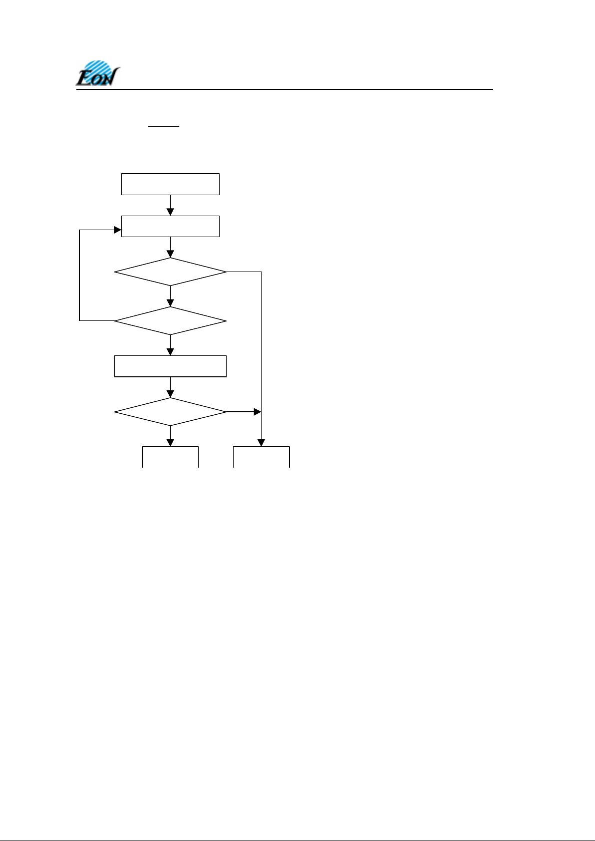
The flowchart for
DATA
Polling (DQ7) is shown on Flowchart 5. The
DATA
Polling (DQ7) timing
diagram is shown in Figure 8.
DQ6
Toggle Bit I
The EN29F002 provides a “Toggle Bit” on DQ6 to indicate to the host system the status of the
embedded programming and erase operations. (See Table 6)
During an embedded Program or Erase operation, suc cessive attem pts to read data from the device
at any address (by toggling
OE
or CE) will result in DQ6 toggling between “zero” and “one”. Once
the embedded Program or Erase operation is com plete, DQ6 will stop toggling and valid data will be
read on the next successive attem pts. During Byte Programming, the Toggle Bit is valid after the
rising edge of the fourth
WE
pulse in the four-cycle sequence. For Chip Erase, the T oggle Bit is valid
after the rising edge of the sixth-cycle sequence. For Sector Erase, the T oggle Bit is valid after the
last rising edge of the Sector Erase Command (30h)
WE
pulse.
In Byte Programming, if the sector being written to is protected, DQ6 will toggle for about
2µs, then stop toggling without the data in the sector having changed. In Sector Erase or Chip
Erase, if all selected sectors ar e protec ted, DQ 6 will toggle for about 100 µs . The chip will then return
to the read mode without changing data in all protected sectors.
Toggling either
CE
or OE will cause DQ6 to toggle.
Page 11

4800 Great America Parkway, Suite 202 Tel: 408-235-8680
Santa Clara, CA 95054 Fax: 408-235-8685
11
EN29F002 / EN29F002N
Rev. C, Issue Date: 2001/ 07/05
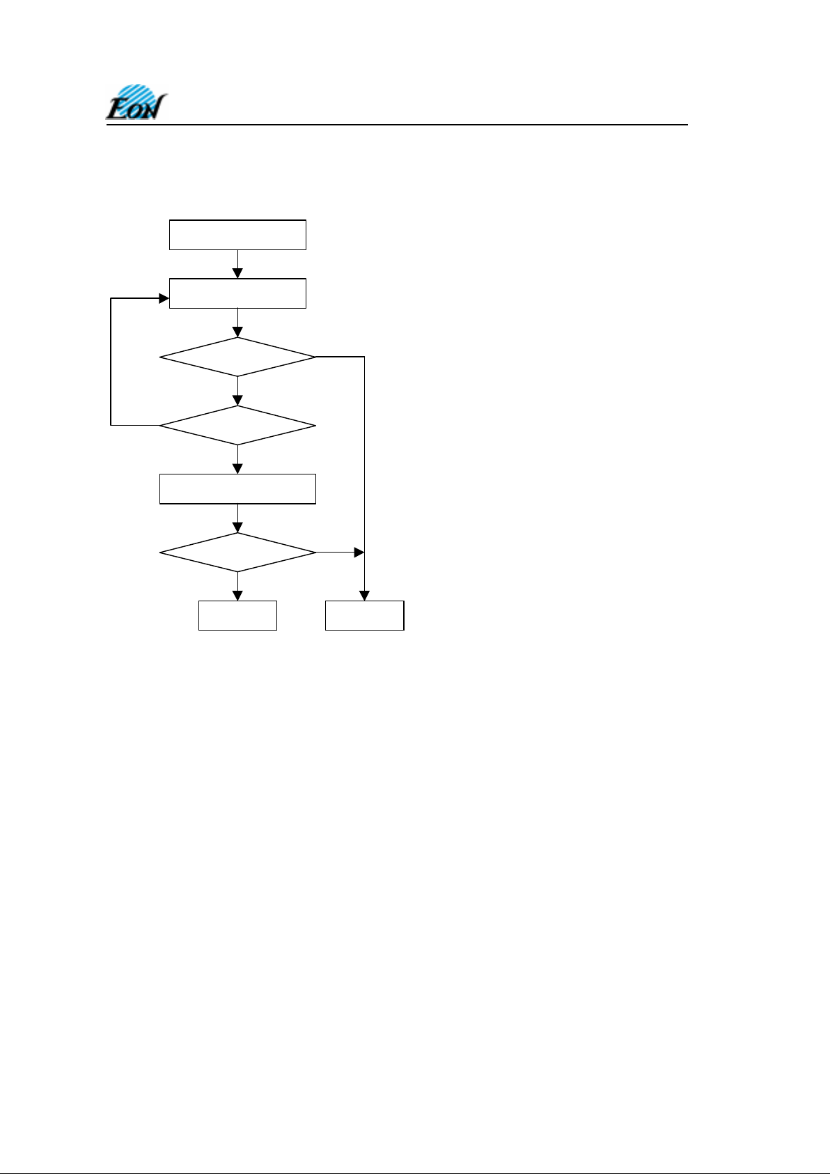
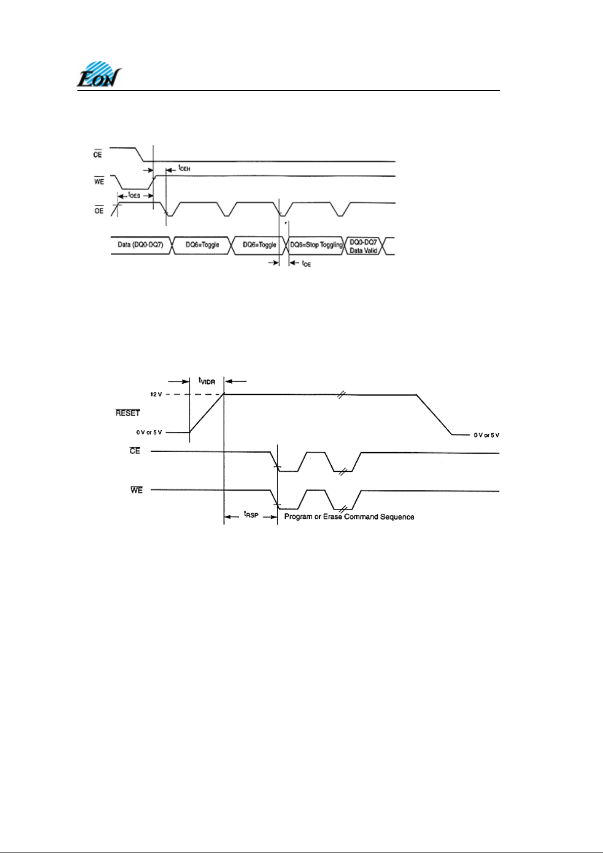
The flowchart for the T oggle Bit (DQ6) is shown in Flowchart 6. The Toggle Bit timing diagram is
shown in Figure 9
.
DQ5
Exceeded Timing Limits
DQ5 will indicate if the program or erase time has exceeded the specified limits (internal pulse
count). Under these conditions DQ5 will produce a “1”. (The Toggle Bit (DQ6) should also be
checked at this time to m ake sure that the DQ5 is not a “ 1” due to the devic e having r eturned to r ead
mode.) This is a failure condition which indicates that the program or erase cycle was not
successfully completed.
DATA
Polling (DQ7), Toggle Bit (D Q6) and Erase Toggle Bit (DQ2) still
function under this condition. Setting the
CE
to VIH will partially power down the device under those
conditions. The
OE
and
WE
pins will control the output disable functions as described in Table 3.
The DQ5 failure c ondition will also appear if the user tries to program a “1” to a location that was
previously programmed to a “0”. In this case, the device goes into Hang or Error mode out and never
completes the Embedded Pr ogram Algorithm. Hence, the system never reads valid data on DQ7
and DQ6 never stops toggling. Once the device exceeds the tim ing limits, DQ5 will indicate a “1”.
Please note that this is not a device failur e condition since the devic e was used incorre ctly. If timing
limits are exceeded, reset the device. (See Table 6)
DQ3
Sector Erase Command Timeout
This device does not support m ultiple sector erase comm ands. DQ3 will go high immediately after
the first 30h command (the sixth write cycle). Any extra 30h commands will be ignored (or taken as a
resume command if erase suspended).
DQ2
Erase Toggle Bit II
In the sector erase operation, DQ2 will toggle with
OE
or CE when a read is attempted within the
sector that is being erased. DQ2 will not toggle if the read address is not within the sector that is
selected to be erased. In the chip erase operation, however, DQ2 will toggle with
OE
or CE
regardless of the addr es s given by the user. This is because all sectors are to be er ased. ( See T able
6)
Page 12
4800 Great America Parkway, Suite 202 Tel: 408-235-8680
Santa Clara, CA 95054 Fax: 408-235-8685
12
EN29F002 / EN29F002N
Rev. C, Issue Date: 2001/ 07/05
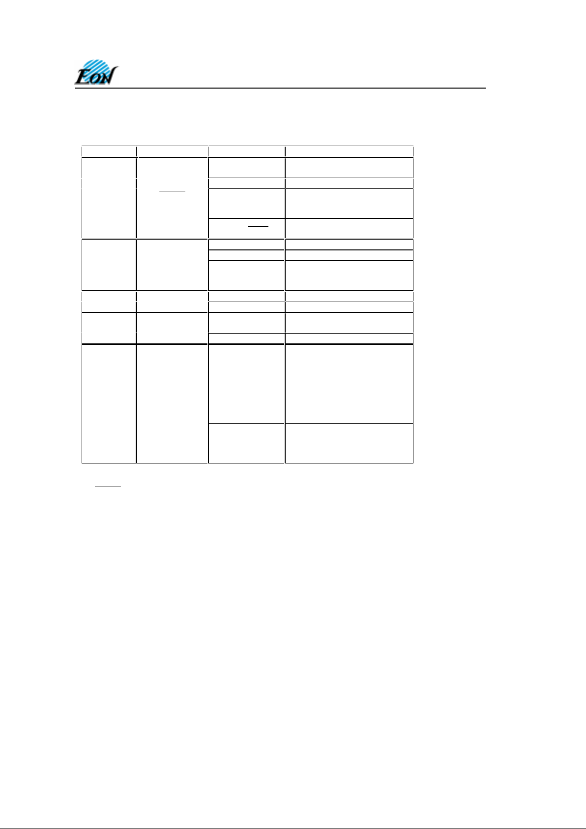
Table 6. Status Register Bits
DQ Name Logic Level Definition
‘1’ Erase Complete or
erase sector in Erase suspend
‘0’ Erase On-Going
7
DATA
POLLING
DQ7
Program Complete or
data of non-erase sector
during Erase Suspend
DQ7
Program On-Going
‘-1-0-1-0-1-0-1-’ Erase or Program On-going
DQ6 Read during Erase Suspend
6
TOGGLE
BIT
‘-1-1-1-1-1-1-1-‘
Erase Complete
5 ERROR BIT ‘1’ Program or Erase Error
‘0’ Program or Erase On-going
3
ERASE
TIME BIT
‘1’ Erase operation start
‘0’ Erase timeout period on-going
‘-1-0-1-0-1-0-1-’
Chip Erase, Erase or Erase
suspend on currently
addressed
sector. (When DQ5=1, Erase
Error due to currently
addressed sector. Program
during Erase Suspend on-
going at current address
2 TOGGLE
BIT
DQ2
Erase Suspend read on
non Erase Suspend Sector
Notes:
DQ7
DATA
Polling: indicates t he P/E C status check during Program or Erase, and on completion before checking bits
DQ5 for Program or Erase Succ ess.
DQ6 Toggle Bit: remains at constant level when P/E operations are c omplete or erase suspend is ac knowledged.
Successive reads output complementary data on DQ6 while program ming or Erase operation are on-going.
DQ5 Error Bit: set to “1’ if failure in programming or erase
DQ3 Sector Erase Command Timeout Bit: Operati on has started. Only possible command is Erase suspend (ES).
DQ2 Toggle Bit: indicates the Erase status and allows identi fication of the erased sector.
Page 13

4800 Great America Parkway, Suite 202 Tel: 408-235-8680
Santa Clara, CA 95054 Fax: 408-235-8685
13
EN29F002 / EN29F002N
Rev. C, Issue Date: 2001/ 07/05
DATA PROTECTION
Power-up Write Inhibit
During power-up, the device automatically resets to READ mode and loc ks out write cycles. Even
with
CE
= VIL, WE = VIL and OE = VIH, the device will not accept com mands on the r ising edge of
WE
.
Low VCC Write Inhibit
During V
CC
power-up or power-down, the EN20F002 locks out write cycles to protect against any
unintentional writes. If V
CC
< V
LKO
, the command register is disabled and all internal program or
erase circuits are disabled. Under this condition, the device will reset to the READ mode. Subsequent
writes will be ignored until V
CC
> V
LKO.
Write “Noise” Pulse Protection
Noise pulses less than 5ns on
OE, CE
or WE will neither initiate a write cycle nor change the
command register.
Logical Inhibit
If
CE
=VIH or WE=VIH, writing is inhibited. To initiate a write cycle, CE and
WE
must be a logical
“zero”. If
CE
, WE, and OE are all logical zero (not recommended usage), it will be cons idered a
write.
Sector Protection/Unprotection
When the device is shipped, all sectors are unprotected. Each sector can be separately protected
against data changes. Using hardware protection circuitry enabled at user’s site with external
programming equipment, both program and erase operations may be disabled for any specified
sector or combination of sectors.
Verification of write protection for a specific sector can be achieved with an Auto Select ID read
command at location 02h where the addres s bits A17 - A13 select the defined sector (see Table 5).
A logical “1” at DQ0 means a protected sector and a logical “0” means an unprotected sector.
The Sector Unprotec t disables sector protection in all sectors in one operation to implem ent code
changes. All s ectors must be placed in protection m ode using the protection algorithm m entioned
above before unprotection can be executed.
Additional details on this feature are provided in a supplement, which can be obtained by contacting a
representative of Eon Silicon Devices, Inc.
Page 14
4800 Great America Parkway, Suite 202 Tel: 408-235-8680
Santa Clara, CA 95054 Fax: 408-235-8685
14
EN29F002 / EN29F002N
Rev. C, Issue Date: 2001/ 07/05
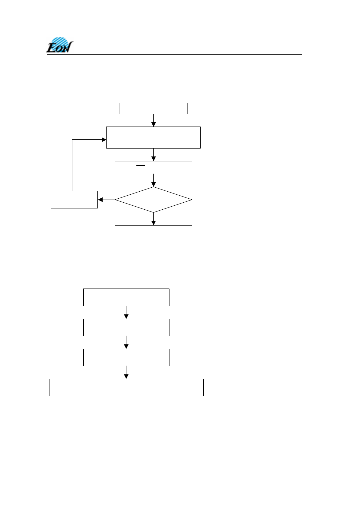
EMBEDDED ALGORITHMS
Flowchart 1. Embedded Program
START
Write Program
Command Sequence
(shown below)
Data Poll Device
Last
Address?
Programming Done
Increment
Address
No
Yes
Flowchart 2. Embedded Program Command Sequence
See the Command Definitions section for more information.
2AAAH / 55H
5555H / AAH
5555H / A0H
PROGRAM ADDRESS / PROGRAM DATA
Page 15
4800 Great America Parkway, Suite 202 Tel: 408-235-8680
Santa Clara, CA 95054 Fax: 408-235-8685
15
EN29F002 / EN29F002N
Rev. C, Issue Date: 2001/ 07/05
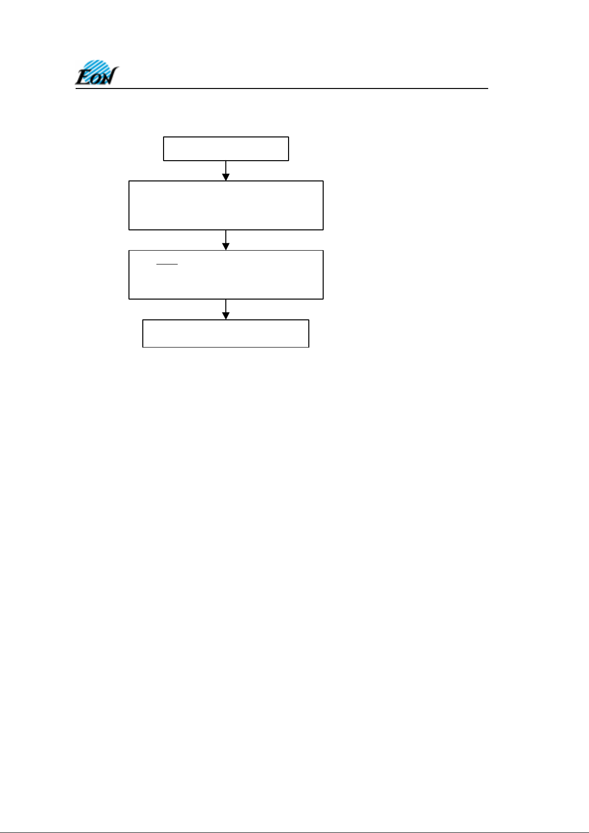
Flowchart 3. Embedded Erase
START
Write Erase
Command Sequence
(shown below)
Data Polling Device or Toggle Bit
Successfully Completed
ERASE Done
Page 16
4800 Great America Parkway, Suite 202 Tel: 408-235-8680
Santa Clara, CA 95054 Fax: 408-235-8685
16
EN29F002 / EN29F002N
Rev. C, Issue Date: 2001/ 07/05
Flowchart 4. Embedded Erase Command Sequence
See the Command Definitions section for more information.
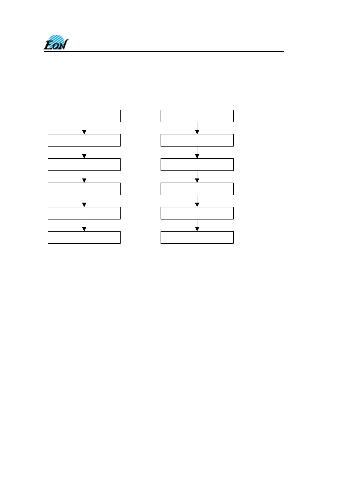
Chip Erase Sector Erase
2AAAH/55H
5555H/AAH
5555H/80H
2AAAH/55H
5555H/AAH
5555H/10H
5555H/AAH
2AAAH/55H
5555H/80H
5555H/AAH
2AAAH/55H
Sector Address/30H
Page 17
4800 Great America Parkway, Suite 202 Tel: 408-235-8680
Santa Clara, CA 95054 Fax: 408-235-8685
17
EN29F002 / EN29F002N
Rev. C, Issue Date: 2001/ 07/05
Flowchart 5. DATAPolling Algorithm
No
No
DQ7 = Data?
DQ5 = 1?
DQ7 = Data?
Yes
Yes
No
Yes
Read Data
Start
Read Data
Fail Pass
Page 18
4800 Great America Parkway, Suite 202 Tel: 408-235-8680
Santa Clara, CA 95054 Fax: 408-235-8685
18
EN29F002 / EN29F002N
Rev. C, Issue Date: 2001/ 07/05
Flowchart 6. Toggle Bit Algorithm
No
Yes
DQ6 = Toggle?
DQ5 = 1?
DQ6 = Toggle?
No
No
Yes
Yes
Read Data
Start
Read Data
Fail Pass
Page 19
4800 Great America Parkway, Suite 202 Tel: 408-235-8680
Santa Clara, CA 95054 Fax: 408-235-8685
19
EN29F002 / EN29F002N
Rev. C, Issue Date: 2001/ 07/05
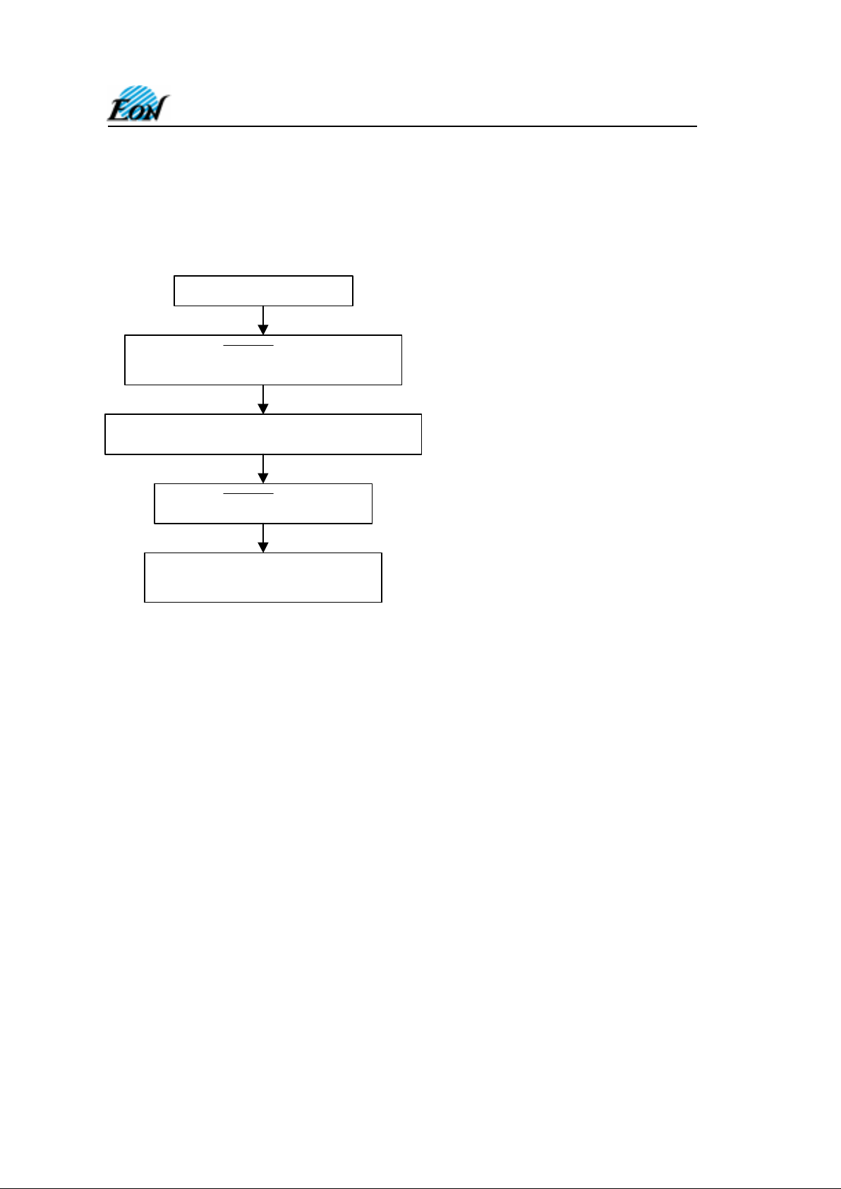
Flowchart 7. Temporary Sector Unprotect Algorithm
(Not available for EN29F002N)
Start
RESET = V
ID
(Note 1)
Perform Erase or Program Operations
RESET = V
IH
Temporary Block Unprot ec t Done
(Note 2)
Notes:
1. All protected sectors unprotected.
2. All previous protected sectors are protected once again.
Page 20
4800 Great America Parkway, Suite 202 Tel: 408-235-8680
Santa Clara, CA 95054 Fax: 408-235-8685
20
EN29F002 / EN29F002N
Rev. C, Issue Date: 2001/ 07/05
ABSOLUTE MAXIMUM RATINGS
Storage Temperature
Plastic Packages . . . . . . . . . . . . . . . –65°C to +125°C
Ambient Temperature
with Power Applied. . . . . . . . . . . . . . –55°C to +125°C
Voltage with Respect to Ground
V
CC
(Note 1) . . . . . . . . . . . . . . . . . . . . –0.5 V to 7.0 V
A9, OE# (Note 2) . . . . . . . . . . . . . . . –0.5 V to 11.5 V
All other pins (Note 1) . . . . . . . . . . . . –0.5 V to Vcc+0.5V
Output Short Circuit Current (Note 3) . . . . . . . . . 200 mA
Notes:
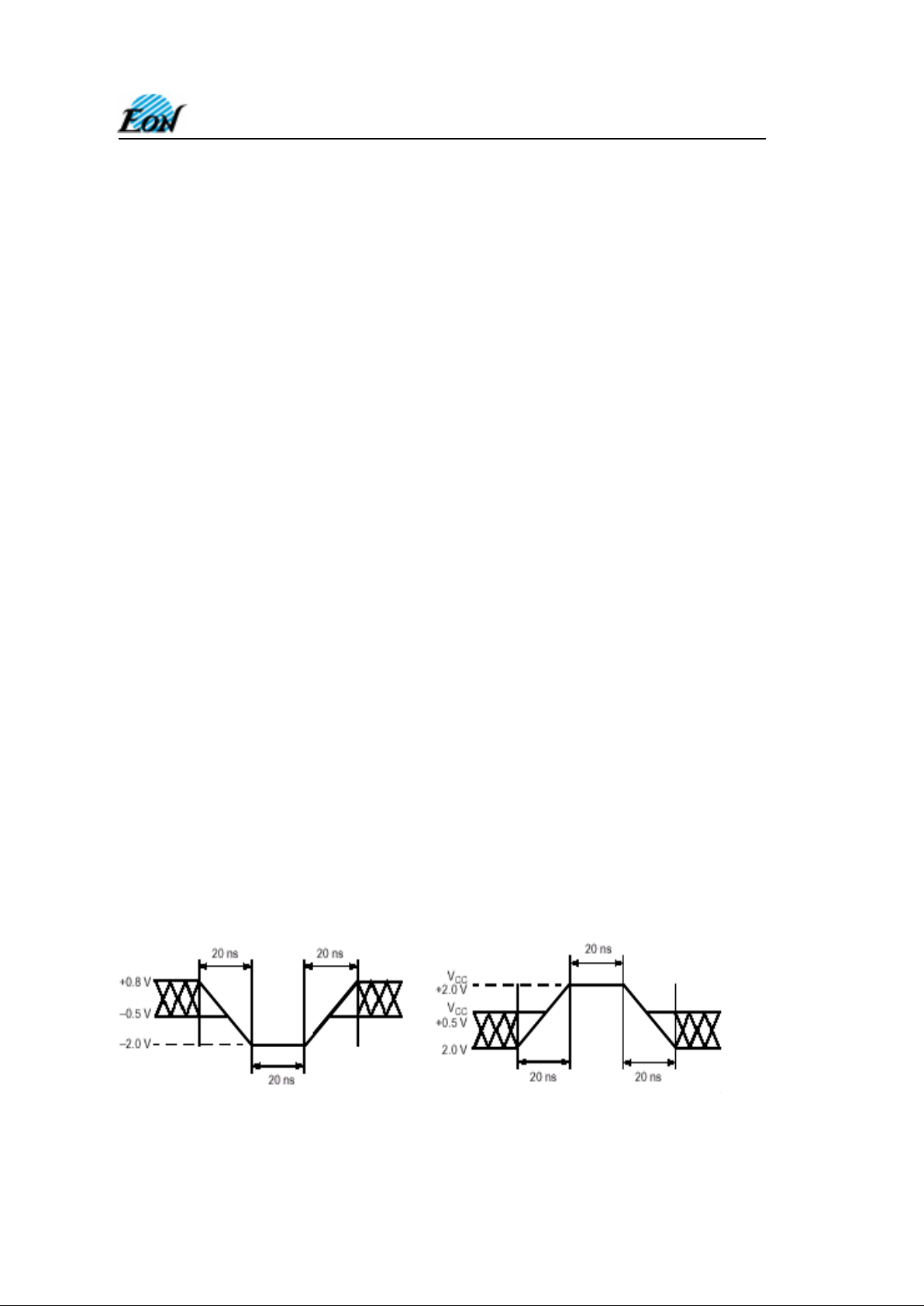
1. Minimum DC voltage on input or I/O pins is –0.5 V. During voltage transitions, inputs may undershoot
V
SS to –1.0V for periods of up to 50 ns and to –2.0 V for periods of up to 20 ns. See Left Figure below.
Maximum DC voltage on input and I/O pins is V
CC + 0.5 V. During voltage transitions, input and I/O
pins may overshoot to V
CC + 2.0 V for periods up to 20 ns. See Right Figure below.
2. Minimum DC input voltage on A9 pin is –0.5 V. During voltage transitions, A9 and OE# may
undershoot V
SS to –1.0V for periods of up to 50 ns and to –2.0 V for periods of up to 20 ns. See Left
Figure. Maximum DC input voltage on A9 and OE# is 11.5 V which may overshoot to 12.5 V for
periods up to 20 ns.
3. No more than one output shorted to ground at a time. Duration of the short circuit should not be
greater than one second. Stresses above those listed under “Absolute Maximum Ratings” may cause
permanent damage to the device. This is a stress rating only; functional operation of the device at
these or any other conditions above those indicated in the operational sections of this specification is
not implied. Exposure of the device to absolute maximum rating conditions for extended periods may
affect device reliability.
OPERATING RANGES
Commercial (C) Devices
Ambient Temperature (T A ) . . . . . . . . . . . 0°C to +70°C
Industrial (I) Devices
Ambient Temperature (T A ). . . . . . . . . . -40°C to +85°C
V
CC
Supply Voltages
V
CC
for ± 5% devices . . . . . . . . . . . . +4.75 V to +5.25 V
V
CC
for ± 10% devices . . . . . . . . . . . +4.50 V to +5.50 V
Operating ranges define those limits between which the
functionality of the device is guaranteed.
Maximum Negative Overshoot Maximum Positive Overshoot
Waveform Waveform
Page 21
4800 Great America Parkway, Suite 202 Tel: 408-235-8680
Santa Clara, CA 95054 Fax: 408-235-8685
21
EN29F002 / EN29F002N
Rev. C, Issue Date: 2001/ 07/05
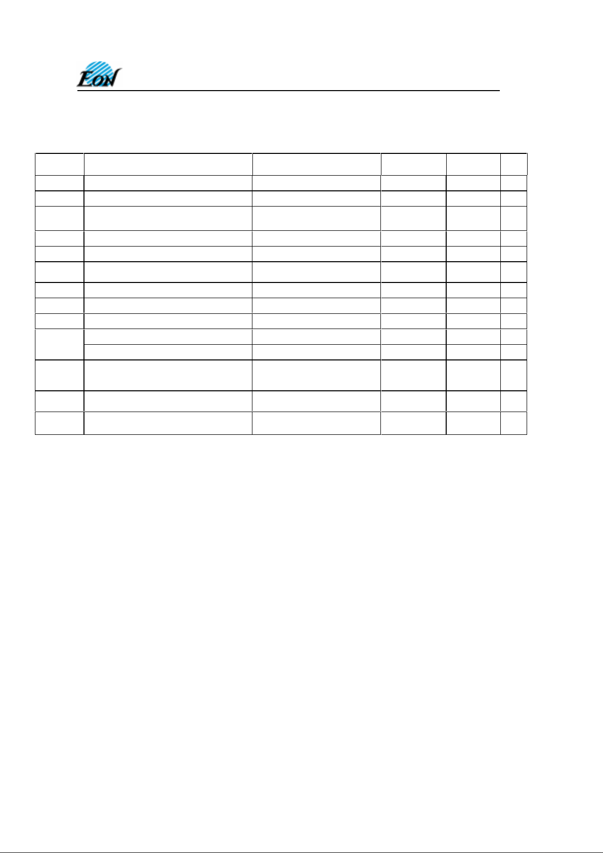
Table 7. DC Characteristics
(Ta = 0°C to 70°C or - 40°C to 85°C; VCC = 5.0V ± 10%)
Symbol Parameter Test Conditions Min Max Uni
t
ILI
Input Leakage Current
0V≤ VIN ≤ Vcc
±5 µA
ILO
Output Leakage Current
0V≤ V
OUT
≤ Vcc
±5 µA
I
CC1
Supply Current (read) TTL Byte
CE# = VIL; OE# = VIH;
f = 6MHz
30 mA
I
CC2
Supply Current (Standby) TTL
CE# = VIH
1.0 mA
I
CC3
Supply Current (Standby) CMOS
(1)
RESET# = CE# = Vcc ± 0.2V 5.0 µA
I
CC4
(2)
Supply Current (Program or Erase)
Byte program, Sector or Chip
Erase in progress
30
mA
VIL
Input Low Voltage -0.5 0.8 V
VIH
Input High Voltage 2 Vcc ± 0.5 V
VOL
Output Low Voltage
IOL = 2 mA
0.45 V
VOH
Output High Voltage TTL
IOH = -2.5 mA
2.4 V
Output High Voltage CMOS
IOH = -100 µA
Vcc - 0.4V V
VID
A9 Voltage (Electronic Signature)
and RESET# Voltage (Temporary
Sector Unprotect)
10.5 11.5 V
I
LIT
A9 and RESET# Current (Electronic
Signature)
A9, RESET# = VID 100 µA
V
LKO
Supply voltage (Erase and
Program lock-out)
3.2 4.2 V
Notes:
(1) RESET# pin input buffer is always enabled so that it draws power if not at full CMOS supply voltages
Page 22
4800 Great America Parkway, Suite 202 Tel: 408-235-8680
Santa Clara, CA 95054 Fax: 408-235-8685
22
EN29F002 / EN29F002N
Rev. C, Issue Date: 2001/ 07/05
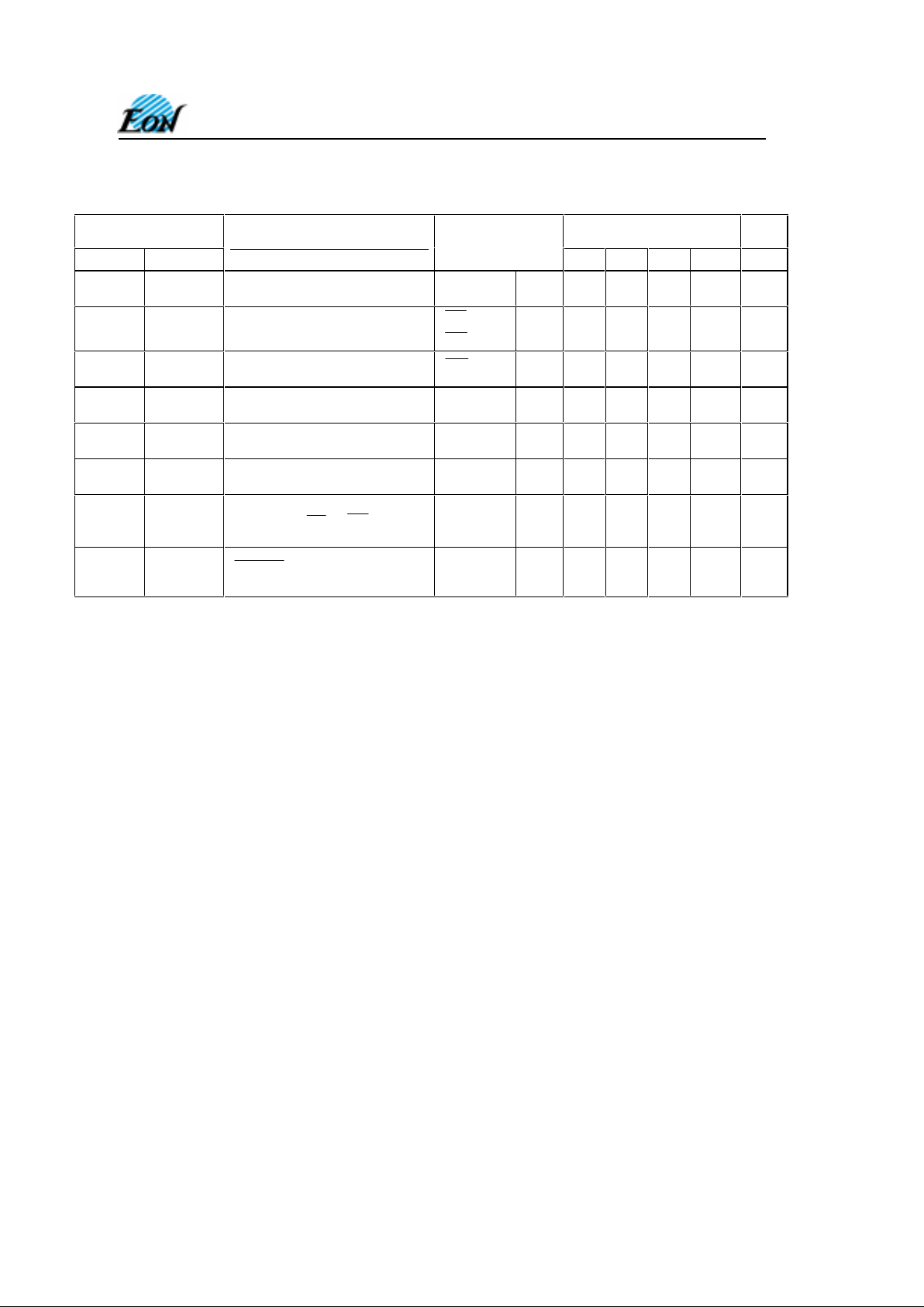
Table 8. AC CHARACTERISTICS
Read-only Operations Characteristics
Parameter
Symbols
Speed Options
JEDEC Standard
Description
Test Setup -45 -55 -70 -90 Unit
t
AVAV
t
RC
Read Cycle Time
Min 45 55 70 90 ns
t
AVQV
t
ACC
Address to Output Delay
CE
= V
IL
OE
= VIL
Max 45 55 70 90 ns
t
ELQV
t
CE
Chip Enable To Output Delay
OE
= VIL
Max 45 55 70 90 ns
t
GLQV
t
OE
Output Enable to Output Delay
Max 25 30 30 35 ns
t
EHQZ
t
DF
Chip Enable to Output High Z
Max 10 15 20 20 ns
t
GHQZ
t
DF
Output Enable to Output High Z
Max 10 15 20 20 ns
t
AXQX
t
OH
Output Hold Time from
Addresses,
CE
or OE,
whichever occurs first
Min 0 0 0 0 ns
t
Ready
RESET
Pin Low to Read
Mode
(n/a for EN29F002N)
Max
20 20 20 20 µs
Notes:
For -45,-55 Vcc = 5.0V ± 5%
Output Load : 1 TTL gate and 30pF
Input Rise and Fall Times: 5ns
Input Rise Levels: 0.0 V to 3.0 V
Timing Measurement Referenc e Level , Input and Output: 1.5 V
For all others: Vcc = 5. 0V ± 10%
Output Load: 1 TTL gate and 100 pF
Input Rise and Fall Times: 20 ns
Input Pulse Levels: 0.45 V to 2.4 V
Timing Measurement Referenc e Level , Input and Output: 0.8 V and 2.0 V
Page 23
4800 Great America Parkway, Suite 202 Tel: 408-235-8680
Santa Clara, CA 95054 Fax: 408-235-8685
23
EN29F002 / EN29F002N
Rev. C, Issue Date: 2001/ 07/05
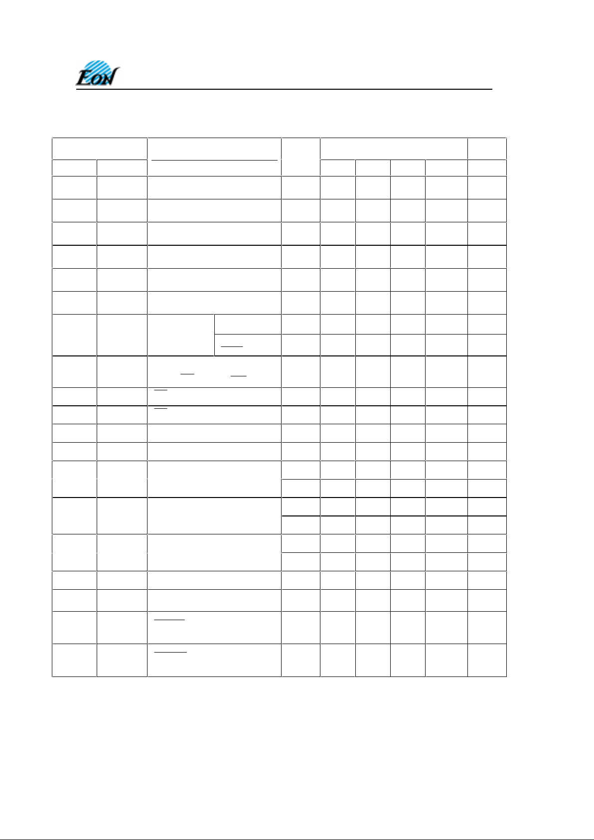
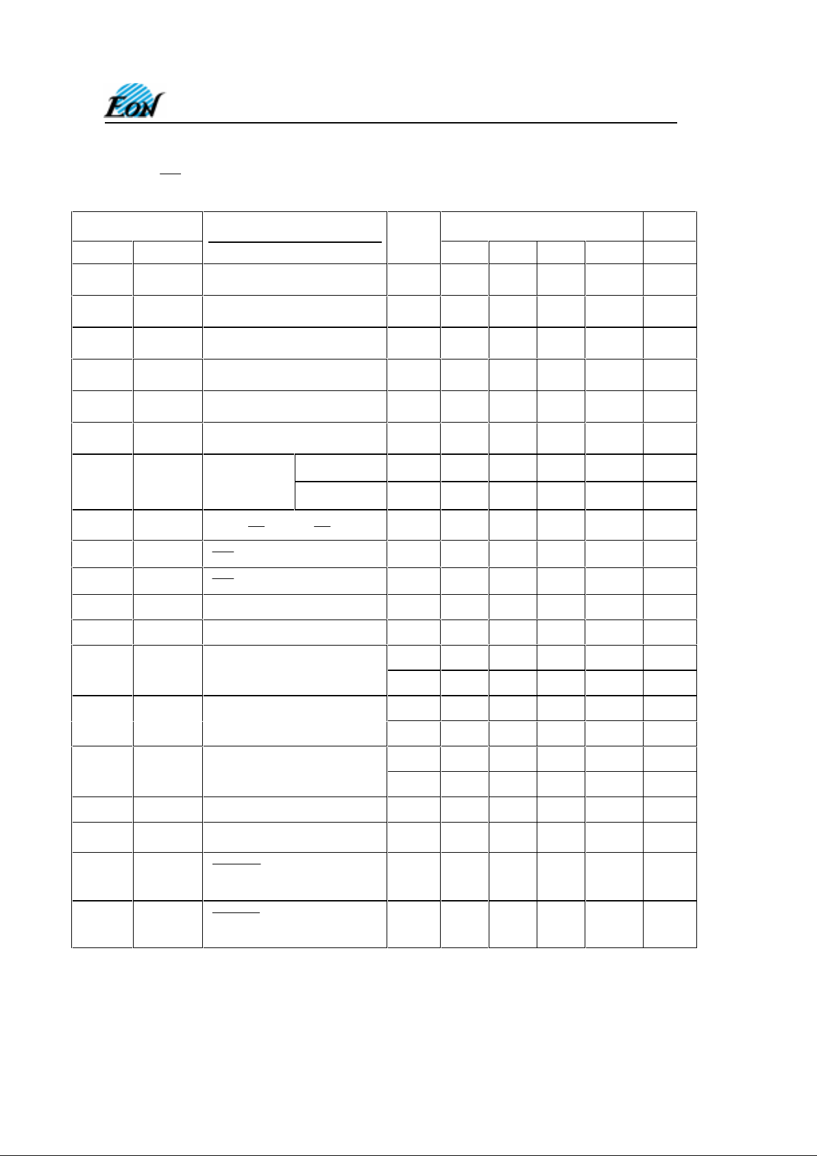
Table 9. AC CHARACTERISTICS
Write (Erase/Program) Operations
Parameter
Symbols
Speed Options
JEDEC Standard
Description
-45 -55 -70 -90 Unit
t
AVAV
t
WC
Write Cycle Time
Min 45 55 70 90 ns
t
AVWL
t
AS
Address Setup Time
Min 0 0 0 0 ns
t
WLAX
t
AH
Address Hold Time
Min 35 45 45 45 ns
t
DVWH
t
DS
Data Setup Time
Min 20 25 30 45 ns
t
WHDX
t
DH
Data Hold Time
Min 0 0 0 0 ns
t
OES
Output Enable Setup Time
Min 0 0 0 0 ns
t
OEH
Output Enable Read
MIn 0 0 0 0 ns
Hold Time Toggle and
DATA
Polling
Min 10 10 10 10 ns
t
GHWL
t
GHWL
Read Recovery Time before
Write (
OE
High to WE Low)
Min
0 0 0 0 ns
t
ELWL
t
CS
CE
SetupTime
Min
0 0 0 0 ns
t
WHEH
t
CH
CE
Hold Time
Min
0 0 0 0 ns
t
WLWH
t
WP
Write Pulse Width
Min
25 30 35 45 ns
t
WHDL
t
WPH
Write Pulse Width High
Min
20 20 20 20 ns
t
WHWH1
t
WHWH1
Programming Operation
Typ
7 7 7 7 µs
Max
200 200 200 200 µs
t
WHWH2
t
WHWH2
Sector Erase Operation
Typ
0.3 0.3 0.3 0.3 s
Max
5 5 5 5 s
t
WHWH3
t
WHWH3
Chip Erase Operation
Typ
3 3 3 3 s
Max
35 35 35 35 s
t
VCS
Vcc Setup Time
Min
50 50 50 50 µs
t
VIDR
Rise Time to V
ID
Min
500 500 500 500 ns
t
RP
RESET
Pulse Width
(n/a for EN29F002N)
Min
500 500 500 500 ns
t
RSP
RESET
Setup Time
(n/a for EN29F002N)
Min
4 4 4 4 µs
Page 24
4800 Great America Parkway, Suite 202 Tel: 408-235-8680
Santa Clara, CA 95054 Fax: 408-235-8685
24
EN29F002 / EN29F002N
Rev. C, Issue Date: 2001/ 07/05
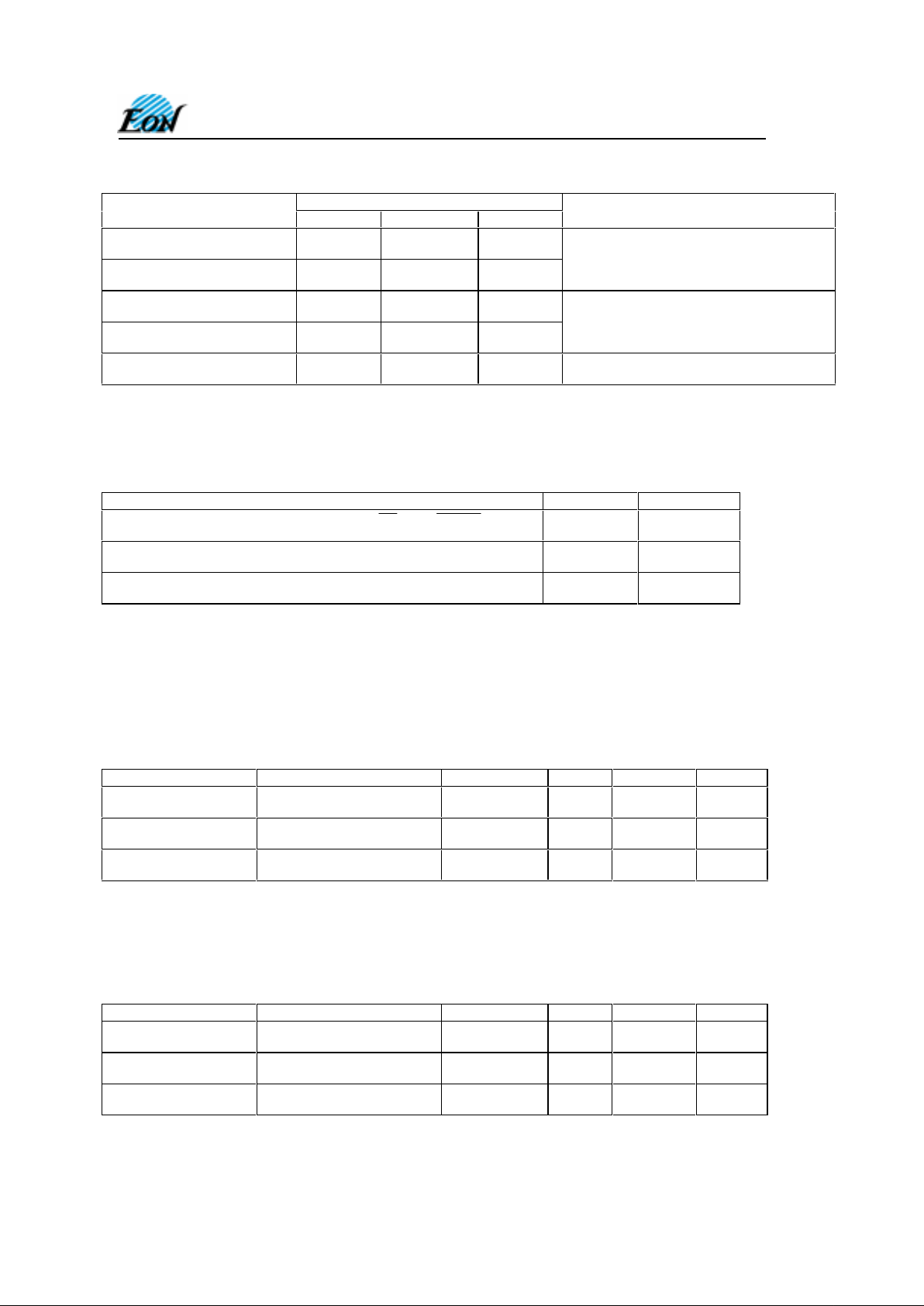
Table 10. AC CHARACTERISTICS
Write (Erase/Program) Operations
Alternate CE Controlled Writes
Parameter
Symbols
Speed Options
JEDEC Standard
Description
-45 -55 -70 -90 Unit
t
AVAV
t
WC
Write Cycle Time
Min 45 55 70 90 ns
t
AVEL
t
AS
Address Setup Time
Min 0 0 0 0 ns
t
ELAX
t
AH
Address Hold Time
Min 35 45 45 45 ns
t
DVEH
t
DS
Data Setup Time
Min 20 25 30 45 ns
t
EHDX
t
DH
Data Hold Time
Min 0 0 0 0 ns
t
OES
Output Enable Setup Time
Min 0 0 0 0 ns
t
OEH
Output Enable Read
0 0 0 0 0 ns
Hold Time Toggle and
Data Polling
10 10 10 10 10 ns
t
GHEL
t
GHEL
Read Recovery Time before
Write (
OE
High to CE Low)
Min
0 0 0 0 ns
t
WLEL
t
WS
WE
SetupTime
Min
0 0 0 0 ns
t
EHWH
t
WH
WE
Hold Time
Min
0 0 0 0 ns
t
ELEH
t
CP
Write Pulse Width
Min
25 30 35 45 ns
t
EHEL
t
CPH
Write Pulse Width High
Min
20 20 20 20 ns
t
WHWH1
t
WHWH1
Programming Operation
Typ
7 7 7 7 µs
Max
200 200 200 200 µs
t
WHWH2
t
WHWH2
Sector Erase Operation
Typ
0.3 0.3 0.3 0.3 s
Max
5 5 5 5 s
t
WHWH3
t
WHWH3
Chip Erase Operation
Typ
3 3 3 3 s
Max
35 35 35 35 s
t
VCS
Vcc Setup Time
Min
50 50 50 50 µs
t
VIDR
Rise Time to V
ID
Min
500 500 500 500 ns
t
RP
RESET
Pulse Width
(n/a for EN29F002N)
Min
500 500 500 500 ns
t
RSP
RESET
Setup Time
(n/a for EN29F002N)
Min
4 4 4 4 µs
Page 25
4800 Great America Parkway, Suite 202 Tel: 408-235-8680
Santa Clara, CA 95054 Fax: 408-235-8685
25
EN29F002 / EN29F002N
Rev. C, Issue Date: 2001/ 07/05
Table 11. ERASE AND PROGRAMMING PERFORMANCE
Limits
Parameter Typ Max Unit Comments
Sector Erase Time 0.3 5 sec Excludes 00H programming prior to
Chip Erase Time 3 35 sec
erasure
Byte Programming Time 7 200 µs Excludes system level overhead
Chip Programming Time 2 5 sec
Erase/Program Endurance 100K cycles
Minimum 100K cycles guaranteed
Table 12. LATCH UP CHARACTERISTICS
Parameter Description Min Max
Input voltage with respect to Vss on A9 and OE, and
RESET
-1.0 V 12.0 V
Input voltage with respect to Vss on all other pins -1.0 V Vcc + 1.0 V
Vcc Current -100 mA 100 mA
Note : These are latch up characteristics and the device should never be put under
these conditions. Refer to Absolute Maximum ratings for the actual operating limits.
Table 13. 32-PIN PLCC PIN CAPACITANCE @ 25°C, 1.0MHz
Parameter Symbol Parameter Description Test Setup Typ Max Unit
CIN
Input Capacitance
VIN = 0
4 6 pF
C
OUT
Output Capacitance
V
OUT
= 0
8 12 pF
C
IN2
Control Pin Capacitance
VIN = 0
8 12 pF
Table 14. 32-PIN TSOP PIN CAPACITANCE @ 25°C, 1.0MHz
Parameter Symbol Parameter Description Test Setup Typ Max Unit
CIN
Input Capacitance
VIN = 0
6 7.5 pF
C
OUT
Output Capacitance
V
OUT
= 0
8.5 12 pF
C
IN2
Control Pin Capacitance
VIN = 0
7.5 9 pF
Page 26

4800 Great America Parkway, Suite 202 Tel: 408-235-8680
Santa Clara, CA 95054 Fax: 408-235-8685
26
EN29F002 / EN29F002N
Rev. C, Issue Date: 2001/ 07/05
Table 15. DATA RETENTION
Parameter Description Test Conditions Min Unit
Minimum Pattern Data Retention Time 150°C 10 Years
125°C 20 Years
Page 27
4800 Great America Parkway, Suite 202 Tel: 408-235-8680
Santa Clara, CA 95054 Fax: 408-235-8685
27
EN29F002 / EN29F002N
Rev. C, Issue Date: 2001/ 07/05
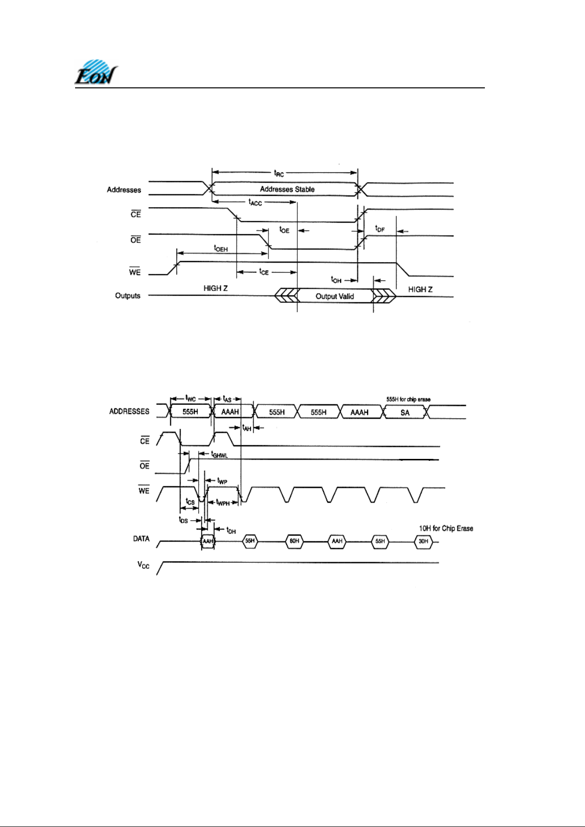
SWITCHING WAVEFORMS
Figure 5. AC Waveforms for READ Operations
Figure 6. AC Waveforms for Chip/Sector Erase Operations
Notes:
1. SA is the sector address for sector erase.
Page 28
4800 Great America Parkway, Suite 202 Tel: 408-235-8680
Santa Clara, CA 95054 Fax: 408-235-8685
28
EN29F002 / EN29F002N
Rev. C, Issue Date: 2001/ 07/05
SWITCHING WAVEFORMS (continued)
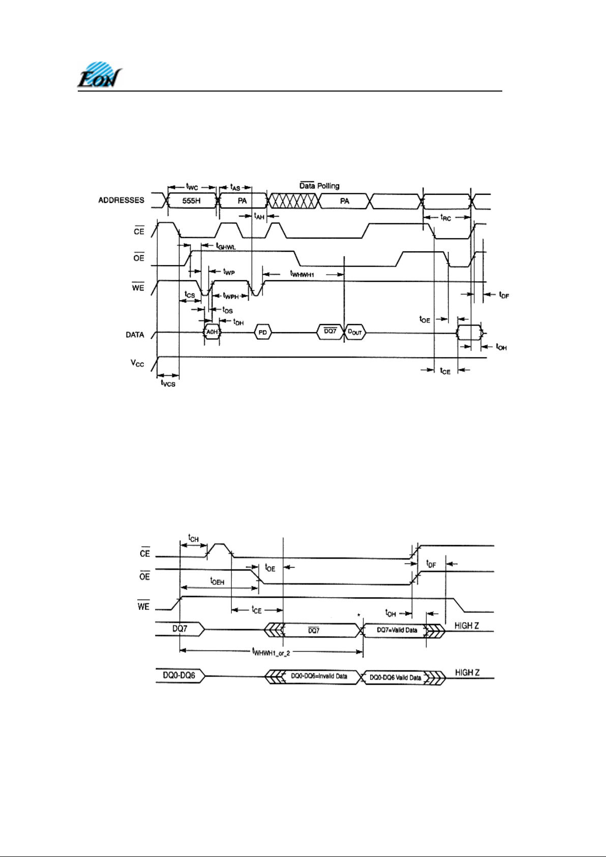
Figure 7. Program Operation Timings
Notes:
1. PA is address of the memory location to be programmed.
2. PD is data to be programmed at byte address.
3. /DQ7 is the output of the complement of the data written to the device.
4. D
OUT
is the output of data written to the device.
5. Figure indicates last two bus cycles of four bus cycle sequence.
Figure 8. AC Waveforms for /DATA Polling During Embedded Algorithm
Operations
Notes:
*DQ
7
= Valid Data (The device has completed the embedded operation).
Page 29
4800 Great America Parkway, Suite 202 Tel: 408-235-8680
Santa Clara, CA 95054 Fax: 408-235-8685
29
EN29F002 / EN29F002N
Rev. C, Issue Date: 2001/ 07/05
Figure 9. AC Waveforms for Toggle Bit During Embedded Algorithm
Operations
Notes:
*DQ6 stops toggling (The device has completed the embedded operation).
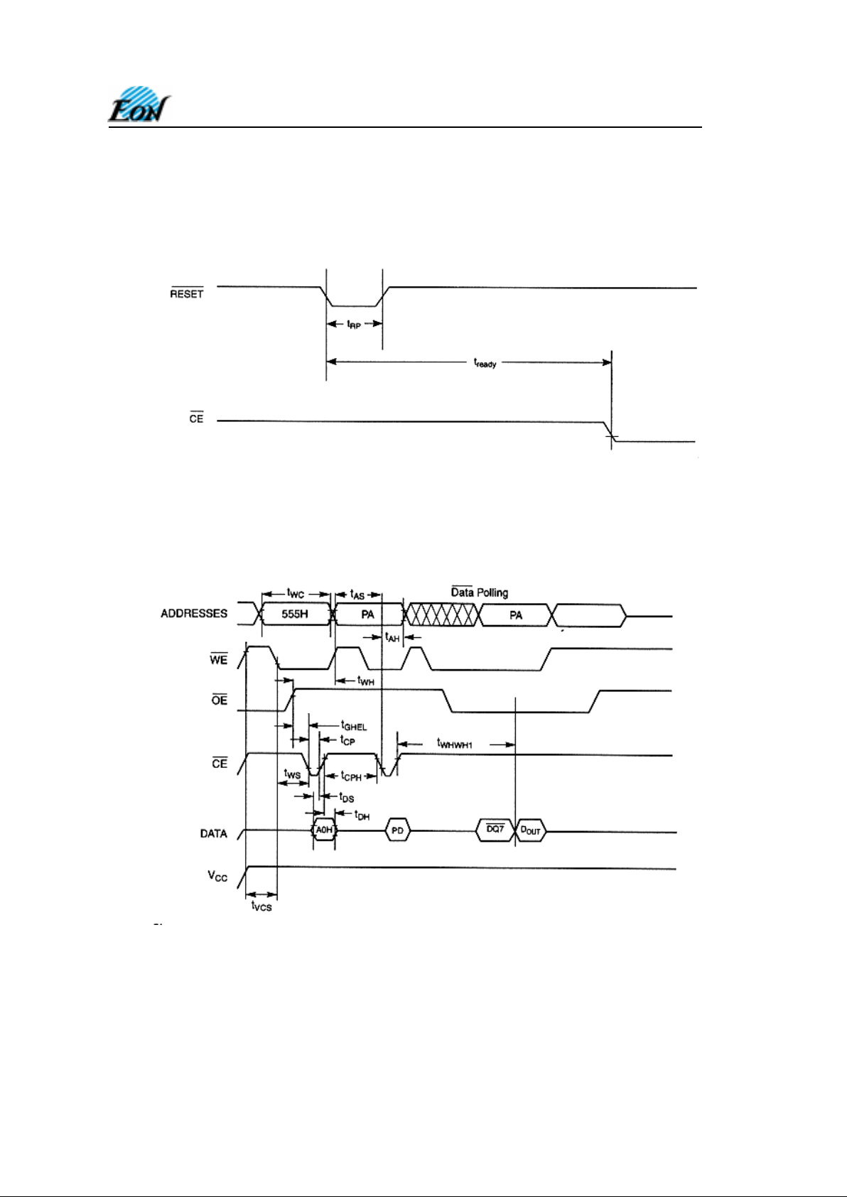
Figure 10. Temporary Sector Unprotect Timing Diagram
Page 30
4800 Great America Parkway, Suite 202 Tel: 408-235-8680
Santa Clara, CA 95054 Fax: 408-235-8685
30
EN29F002 / EN29F002N
Rev. C, Issue Date: 2001/ 07/05
SWITCHING WAVEFORMS (continued)
Figure 11. /RESET Timing Diagram
Figure 12. Alternate /CE Controlled Write Operation Timings
Notes:
1. PA is address of the memory location to be programmed.
2. PD is data to be programmed at byte address.
3. /DQ7 is the output of the complement of the data written to the device.
4. D
OUT
is the output of data written to the device.
5. Figure indicates last two bus cycles of four bus cycle sequence.
Page 31

4800 Great America Parkway, Suite 202 Tel: 408-235-8680
Santa Clara, CA 95054 Fax: 408-235-8685
31
EN29F002 / EN29F002N
Rev. C, Issue Date: 2001/ 07/05
ORDERING INFORMATION
EN29F002 T - 45 P I
TEMPERATURE RANGE
(Blank) = Commercial (0°C to +70°C)
I = Industrial (-40°C to +85°C)
PACKAGE
P = 32 Plastic DIP
J = 32 Plastic PLCC
T = 32 Plastic TSOP
SPEED
45 = 45ns
55 = 55ns
70 = 70ns
90 = 90ns
BOOT BLOCK ARCHITECTURE
T = Top Block
B = Bottom Block
BASE PART NUMBER
EN = EON Silicon Devices
29F = FLASH, 5V
002 = 256K x 8
(Blank) = with
RESET
function
N = without
RESET
function
Page 32

4800 Great America Parkway, Suite 202 Tel: 408-235-8680
Santa Clara, CA 95054 Fax: 408-235-8685
32
EN29F002 / EN29F002N
Rev. C, Issue Date: 2001/ 07/05
Revisions List
A:
Preliminary
B (2001.07.03):
Table 7. Icc3 is with RESET# pin at full CMOS levels
Pg. 13 Logical Inhibit section now says that if
CE
,
WE
, and OE are all logical zero
(not recommended usage), it will be considered a write.
VID is everywhere changed to be VID =11.5 ± 0.5V
C (2001.07.05):
VID is everywhere changed to be VID =11.0 ± 0.5V
“block” changed to “sector” everywhere appropriate.
Deleted Sector Un/Protect flow charts (we have a supplement for that)
RESET# = VID and not VPP on first page.
LACTHUP >= 200mA line removed from first page
Chip erase and Sector Erase command descriptions modified.
DQ7,DQ5,DQ3 status polling de scriptions modified.
Table 7 and Table 12 modified
Absolute Maximum Ratings section added
 Loading...