

Datasheet EN27C02070T, EN27C02070PI, EN27C02070P, EN27C02070JI, EN27C02070J Datasheet (EON)
...Page 1
EN27C020
4800 Great America Parkway Ste 202 Tel: 408-235-8680
Santa Clara, CA. 95054 Fax: 408-235-8685
Preliminary
1
FEATURES
• Fast Read Access Time:
-45, -55, -70, and -90ns
• Single 5V Power Supply
• Programming Voltage +12.75V
• QuikRite
TM
Programming Algorithm
• Typical programming time 20µs
• Low Power CMOS Operation
• 1µA Standby (Typical)
• 30mA Operation (Max.)
• CMOS- and TTL-Compatible I/O
• High-Reliability CMOS Technology
• Latch-Up Immunity to 100mA
from -1V to V
CC
+ 1V
• Two-Line Control (
OE & CE)
• Standard Product Identification Code
• JEDEC Standard Pinout
• 32-pin PDIP
• 32-pin PLCC
• 32-pin TSOP (Type 1)
• Commercial and Industrial Temperature
Ranges
GENERAL DESCRIPTION
The EN27C020 is a low-power 2-Megabit, 5V-only one-time-programmable (OTP) read-only
memory (EPROM). Organi zed into 256K words with 8 bits per word, it feat ures QuikRi te
TM
single-
address location program m i ng, typi cal l y at 20µs per byte. Any byte c an be accessed in less t han
45ns, eliminating the need for W AIT states in high-performance microprocessor systems. The
EN27C020 has separate Output Enable (
OE ) and Chip Enable ( CE ) controls which eli minate
bus contention issues.
FIGURE 1. PDIP
Pin Name Function
A0-A17 Addresses
DQ0-DQ7 Outputs
Chip Enable
Output Enable
Program Strobe
A17
EN27C020 2Megabit EPROM (256K x 8)
Page 2
EN27C020
4800 Great America Parkway Ste 202 Tel: 408-235-8680
Santa Clara, CA. 95054 Fax: 408-235-8685
Preliminary
2
FIGURE 2. TSOP
FIGURE 3. PLCC
TSOP
EN27C020
A17
PLCC Top V iew
A12 A16 Vcc A17
A15 Vpp PGM
Page 3
EN27C020
4800 Great America Parkway Ste 202 Tel: 408-235-8680
Santa Clara, CA. 95054 Fax: 408-235-8685
Preliminary
3
FIGURE 4. BLOCK DIAGRAM
FUNCTIONAL DESCRIPTION
THE QUIKRITETM PROGRAMMING OF THE EN27C020
When the EN27C020 is delivered, the chip has all 2M bits in the “ONE”, or
HIGH state. “ZEROs” are loaded into the EN27C020 through the procedure of programming.
The programming mode is entered when 12.75 ± 0.25V is applied to the V
PP
pin, OE is at V
IH
, and CE and PGM are at VIL. For programm ing, the data to be program med is applied
with 8 bits in parallel to the data pins.
The QUIKRITE
TM
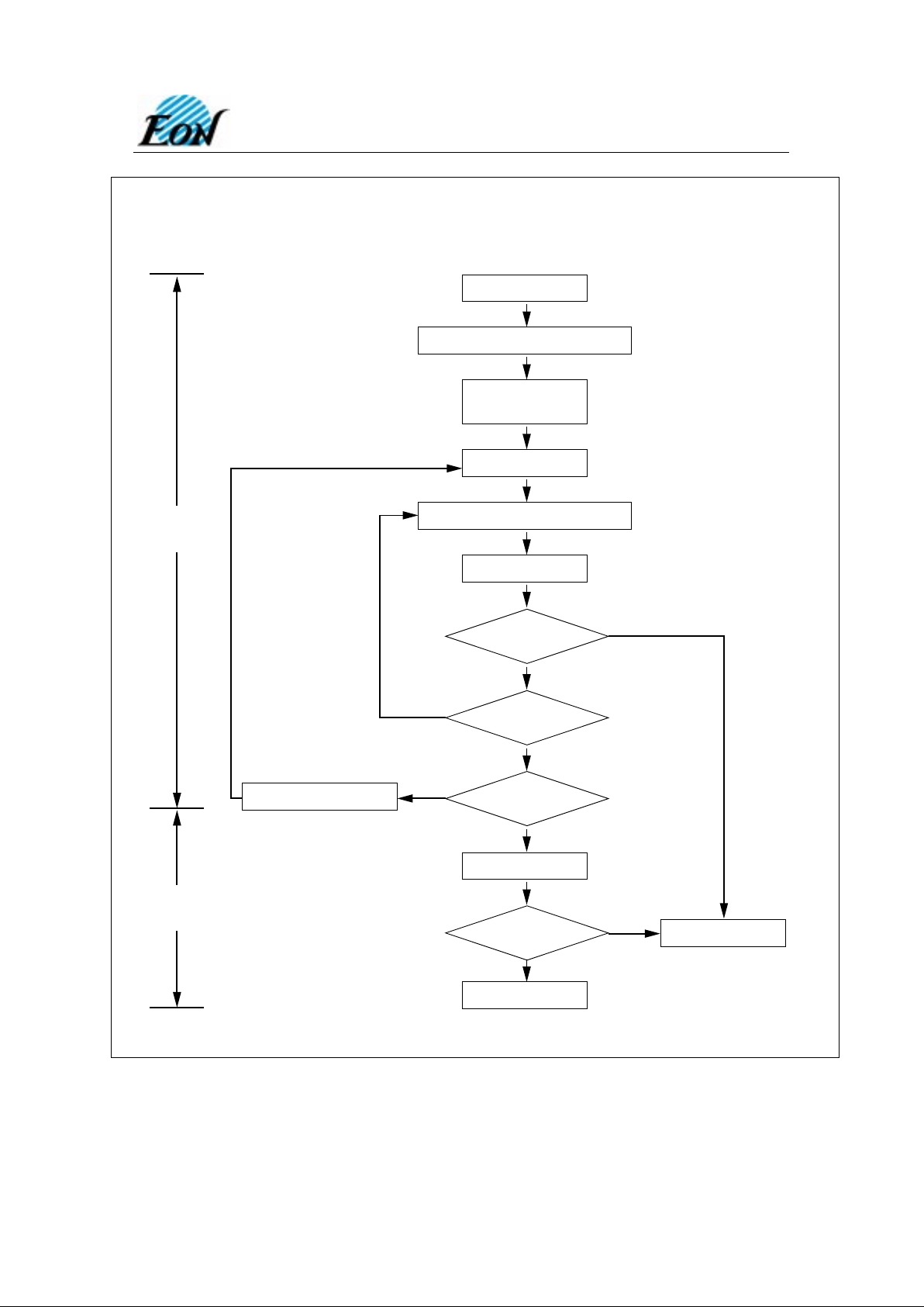
programming flowchart in Figure 5 shows Eon’s interactive programming
algorithm. The interactive algorithm reduces programming time by using 20 µs to 100 µs
programming pulses and giving each address only as many pulses as is necessary in order to
reliably program the data. After each pulse is applied to a given address, the data in that
address is verified. If the data is not verified, additional pulses are given until it is verified or
until the maximum number of pulses is reached. This process is repeated while sequencing
through each address of the EN27C020. This part of the programming algorithm is done at
V
CC
= 6.25V to assure that each EPROM bit is programmed to a sufficiently high threshold
voltage. This ensures that all bits have sufficient margin. After the final address is
completed, the entire EPROM memory is read at VCC = V
PP
= 5.25 ± 0.25V to verify the
entire memory.
CONTROL
LOGIC
INPUT/
OUTPUT
BUFFERS
Y-DECODER
X-DECODER
Y-SELECT
2M BIT
CELL
MATRIX
Vcc
Vpp
Vss
A0 - A17
ADDRESS
INPUTS
DQ0 - DQ7
8
1024
2048
CE
PGM
OE
Page 4

EN27C020
4800 Great America Parkway Ste 202 Tel: 408-235-8680
Santa Clara, CA. 95054 Fax: 408-235-8685
Preliminary
4
PROGRAM INHIBIT MODE
Programming of multiple EN27C020 in parallel with different data is also easily
accomplished by using the Program Inhibit Mode. Except for
CE , all like inputs of the
parallel EN27C020 may be common. A TTL low-level program pulse applied to an
EN27C020
CE input with V
PP
= 12.75 ± 0.25V PGM LOW, and OE HIGH will program that
EN27C020. A high -level
CE input inhibits the other EN27C020 from being programmed.
PROGRAM VERIFY MODE
Verification should be performed on the programmed bits to determining that they were
correctly programmed. The verification should be performed with
OE and CE at V
IL
,
PGMat VIH, and VPP at it programming voltage.
AUTO PRODUCT IDENTIFICATION
The Auto Product Identification mode allows the reading out of a binary code from an EPROM
that will identify its manufacturer and type. This mode is intended for use by programming
equipment for the purpose of automatically matching the device to be programmed with its
corresponding programming algorithm. This mode is functional in the 25°C ± 5°C ambient
temperature range that is required when programming the EN27C020.
To activate this mode, the programming equipment must force 12.0 V ± 0.5V on address line A9
of the EN27C020. Two identifier bytes may then be sequenced from the device outputs by
toggling address line A0 from V
IL
to VIH, when A1 = VIH. All other address lines must be held at
V
IL
during Auto Product Identification mode.
Byte 0 (A0 = V
IL
) represents the manufacturer code, and byte 1 (A0 = VIH), the device code. For
the EN27C020, these two identifiers bytes are given in the Mode Select Table. All identifiers for
manufacturer and device codes will possess odd parity, with the MSB (DQ7) defined as the
parity bit.
When A1 = VIL, the EN27C020 will read out the binary code of 7F, continuation code,
to signify the unavailability of manufacturer ID codes.
Page 5

EN27C020
4800 Great America Parkway Ste 202 Tel: 408-235-8680
Santa Clara, CA. 95054 Fax: 408-235-8685
Preliminary
5
READ MODE
The EN27C020 has two control functions, both of which must be logically satisfied in order to
obtain data at the outputs. Chip Enable (
CE ) is the power control and should be used for
device selection. Output Enable (
OE ) is the output control and should be used to gate data
to the output pins, independent of device selection. Assuming that addresses are stable,
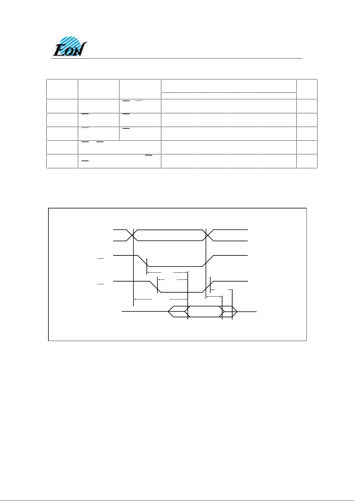
address access time (t
ACC
) is equal to the delay from CE to output (tCE) . Data is available at
the outputs (t
OE
) after the falling edge of OE , assuming the CE has been LOW and
addresses have been stable for at least t
ACC
- tOE.
STANDBY MODE
The EN27C020 has CMOS standby mode which reduces the maximum V
CC
current to 20µA.
It is placed in CMOS standby when
CE is at V
CC
± 0.3 V. The EN27C020 also has a TTL-
standby mode which reduces the maximum V
CC
current to 1.0 mA. It is placed in TTL-
standby when
CE is at V
IH
. When in standby mode, the outputs are in a high-impedance
state, independent of the
OE input.
TWO-LINE OUTPUT CONTROL FUNCTION
To accommodate multiple memory connections, a two-line control function is provided to
allow for:
1. Low memory power dissipation,
2. Assurance that output bus contention will not occur.
It is recommended that
CE be decoded and used as the primary device-selection function,
while
OE be made a common connection to all devices in the array and connected to the
READ line from the system control bus. This assures that all deselected memory devices are in
their low-power standby mode and that the output pins are only active when data is desired
from a particular memory device.
SYSTEM CONSIDERATIONS
During the switch between active and standby conditions, transient current peaks are produced
on the rising and falling edges of Chip Enable. The magnitude of these transient current peaks
is dependent on the output capacitance loading of the device. At a minimum, a 0.1µF ceramic
capacitor (high frequency, low inherent inductance) should be used on each device between
VCC and VSS to minimize transient effects. In addition, to overcome the voltage drop caused
by the inductive effects of the printed circuit board traces on EPROM arrays, a 4.7µF bulk
electrolytic capacitor should be used between VCC and VSS for each eight devices. The
location of the capacitor should be close to where the power supply is connected to the array.
Page 6
EN27C020
4800 Great America Parkway Ste 202 Tel: 408-235-8680
Santa Clara, CA. 95054 Fax: 408-235-8685
Preliminary
6
MODE SELECT TABLE
Mode CE OE PGM A0 A1 A9
V
PP
Output
Read
V
IL
V
IL
X
(2)
XX X
V
CC
D
OUT
Output Disable
V
IL
V
IH
XXXX
V
CC
High Z
Standby (TTL)
V
IH
XX XXX
V
CC
High Z
Standby (CMOS)
V
CC
± 0.3V
XX XXX
V
CC
High Z
Program
(4)
V
IL
V
IH
V
IL
XX X
V
PP
D
IN
Program Verify
V
IL
V
IL
V
IH
XX X
V
PP
D
OUT
Program Inhibit
V
IH
XX XXX
V
PP
High Z
Manufacturer Code
(3)
V
IL
V
IL
X
V
IL
V
IH
VH
(1)
V
CC
1C
Device Code
(3)
V
IL
V
IL
X
V
IH
V
IH
VH
(1)
V
CC
02
NOTES:
1) VH = 12.0V ± 0.5V
2) X = Either VIH or V
IL
3) For Manufacturer Code and Device Code, A1 = V
IH
When A1 = VIL, both codes will read 7F
4) See DC Programming Characteristics for V
PP
voltage during programming
EON’S STANDARD PRODUCT IDENTIFICATION CODE
Pins
Hex
Data
Code
A0 A1 DQ7 DQ6 DQ5 DQ4 DQ3 DQ2 DQ1 DQ0
Manufacturer
01000111001C
Device Type
110000001002
Continuation
00011111117F
10011111117F
Page 7
EN27C020
4800 Great America Parkway Ste 202 Tel: 408-235-8680
Santa Clara, CA. 95054 Fax: 408-235-8685
Preliminary
7
FIGURE 5. QUIKRITETM PROGRAMMING FLOW CHART
START
X = 0
INCREMENT X
X = 25?
YES
YES
PASS
PASS
NO
FAIL
FAIL
NO
FAIL
VCC = VPP = 5.25V
DEVICE PASSED
DEVICE FAILED
VCC = 6.25V
VPP = 12.75V
INTERACTIVE
SECTION
VERIFY
SECTION
ADDRESS = FIRST LOCATION
PROGRAM ONE 10µs PULSE
INCREMENT ADDRESS
VERIFY BYTE?
VERIFY ALL BYTES?
LAST ADDRESS
20
NOTE 1: Either 100µs or 20µs pulse.
Page 8

EN27C020
4800 Great America Parkway Ste 202 Tel: 408-235-8680
Santa Clara, CA. 95054 Fax: 408-235-8685
Preliminary
8
ABSOLUTE MAXIMUM RATINGS
Storage Temperature
-65ÝC to +125ÝC
Ambient Temperature
with Power Applied -40ÝC to +85ÝC
Voltage with Respect to V
SS
All pins except A9, VPP, V
CC
-0.6V to VCC + 0.5V
A9, V
PP
-0.6V to +13.5V
V
CC
-0.6V to +7.0V
OPERATING RANGES
Commercial (C)
Case Temperature(Tc) 0ÝC to +70ÝC
Industrial (I)
Case Temperature(Tc) -40ÝC to +85ÝC
Supply READ Voltages
+4.50V to +5.5V
(Functionality is guaranteed between these limits)
Stresses abov e t hos e s hown abov e may c ause permanent damage to the device. This is a s tres s r ating only and oper ation
above these specifications for extended periods may affect device reliability. Operatio n outside the "OPERATING RANGES"
shown above voids any and all warranty provisions.
DC CHARACTERISTICS FOR READ OPERATION
Symbol Parameter Min. Max. Unit Conditions
V
OH
Output High Voltage 2.4 V IOH = -0.4mA
V
OL
Output Low Voltage 0.45 V IOL = 2.1mA
V
IH
Input High Voltage 2.0
V
CC
+0.5
V
V
IL
Input Low Voltage -0.3 0.8 V
I
LI
Input Leakage Current -5 5
µA
VIN = 0 to 5.5V
I
LO
Output Leakage Current -10 10
µA
V
OUT
= 0 to 5.5V
I
CC3
VCC Power -Down Current 10
µA CE = V
CC
± 0.3V
I
CC2
VCC Standby Current 1.0 mA
CE = V
IH
I
CC1
VCC Active Current 30 mA
CE = V
IL
, f=5MHz,
L
OUT
= 0mA
I
PP
VPP Supply Current Read 100
µA
CE = OE = V
IL
,
V
PP
= 5.5V
CAPACITANCE
Symbol Parameter Typ. Max. Unit Conditions
C
IN
Input Capacitance 8 12 pF VIN = 0V
C
OUT
Output Capacitance 8 12 pF V
OUT
= 0V
C
VPP
VPP Capacitance 18 25 pF VPP = 0V
Page 9
EN27C020
4800 Great America Parkway Ste 202 Tel: 408-235-8680
Santa Clara, CA. 95054 Fax: 408-235-8685
Preliminary
9
AC CHARACTERISTICS FOR READ OPERATION
EN27C020
-45 -55 -70 -90
Symbol Parameter Condition Min Max Min Max Min Max Min Max Unit
tACC (3) Address to
Output Delay
CE = OE = V
IL
45 55 70 90 ns
tCE (2) CE to Output
Delay
OE = V
IL
45 55 70 90 ns
tOE (2, 3) OE to Output
Delay
OE = V
IL
25 25 30 35 ns
tDF (4, 5) OE or CE High to Output Float,
whichever occurred first
20 20 25 25 ns
tOH Output Hold from Address, CE
or OE, whichever occurred first
0000 ns
Note: Please contact Marketing Department for other speed requirements.
FIGURE 6. AC WAVEFORMS FOR READ OPERATION
CE
ADDRESS ADDRESS VALID
OE
OUTPUT
OUTPUT
VALID
tCE
tACC
HIGH Z
tOE
tDF
tOH
Page 10
EN27C020
4800 Great America Parkway Ste 202 Tel: 408-235-8680
Santa Clara, CA. 95054 Fax: 408-235-8685
Preliminary
10
FIGURE 7. OUTPUT TEST WAVEFORMS AND MEASUREMENTS
AC
DRIVING
LEVELS
AC
MEASUREMENT
LEVEL
3.0V
1.5V
0.0V
tR, tF < 5 ns (10% to 90%)
AC
DRIVING
LEVELS
AC
MEASUREMENT
LEVEL
OUTPUT
PIN
Note: CL = 100pF including
jig capacitance, except for the
-45 and -55 devices, where
CL = 30pF.
1.3V
(1N914)
3.3K
CL
2.4V
0.8
2.0
0.45V
tR, tF < 20 ns (10% to 90%)
45 and 55 devices:
Output Test Load
70 and 90 devices:
DC PROGRAMMING CHARACTERISTICS
Test Limits
Symbol Parameter Conditions Min. Max Units
I
LI
Input Load Current V
IN = VIL, VIH
5.0
µA
V
IL
Input Low Level -0.5 0.8 V
V
IH
Input High Level 0.7 V
CC
V
CC
+ 0.5 V
V
OL
Output Low Voltage I
OL =
2.1 mA 0.45 V
V
OH
Output High Voltage
I
OH =
-400 µA
2.4 V
I
CC2
VCC Supply Current 40 mA
I
PP2
V
PP
Supply Current CE = PGM = V
IL,
10 mA
V
ID
A9 Product Identification Voltage 11.5 12.5 V
Page 11
EN27C020
4800 Great America Parkway Ste 202 Tel: 408-235-8680
Santa Clara, CA. 95054 Fax: 408-235-8685
Preliminary
11
FIGURE 8. PROGRAMMING WAVEFORMS
ADDRESS
VIH
VIL
ADDRESS STABLE
DATA IN
PROGRAM
READ
(VERIFY)
DATA
VIH
VIL
DATA OUT
VALID
V
CC
6.5V
5.0V
V
PP
13.0V
5.0V
CE
VIH
VIL
PGM
VIH
VIL
OE
VIH
VIL
tAS tOE
tPRT
tDS tDH
tVCS
tVPS
tPW
tOES
tCES
tAH
tDFP
Page 12
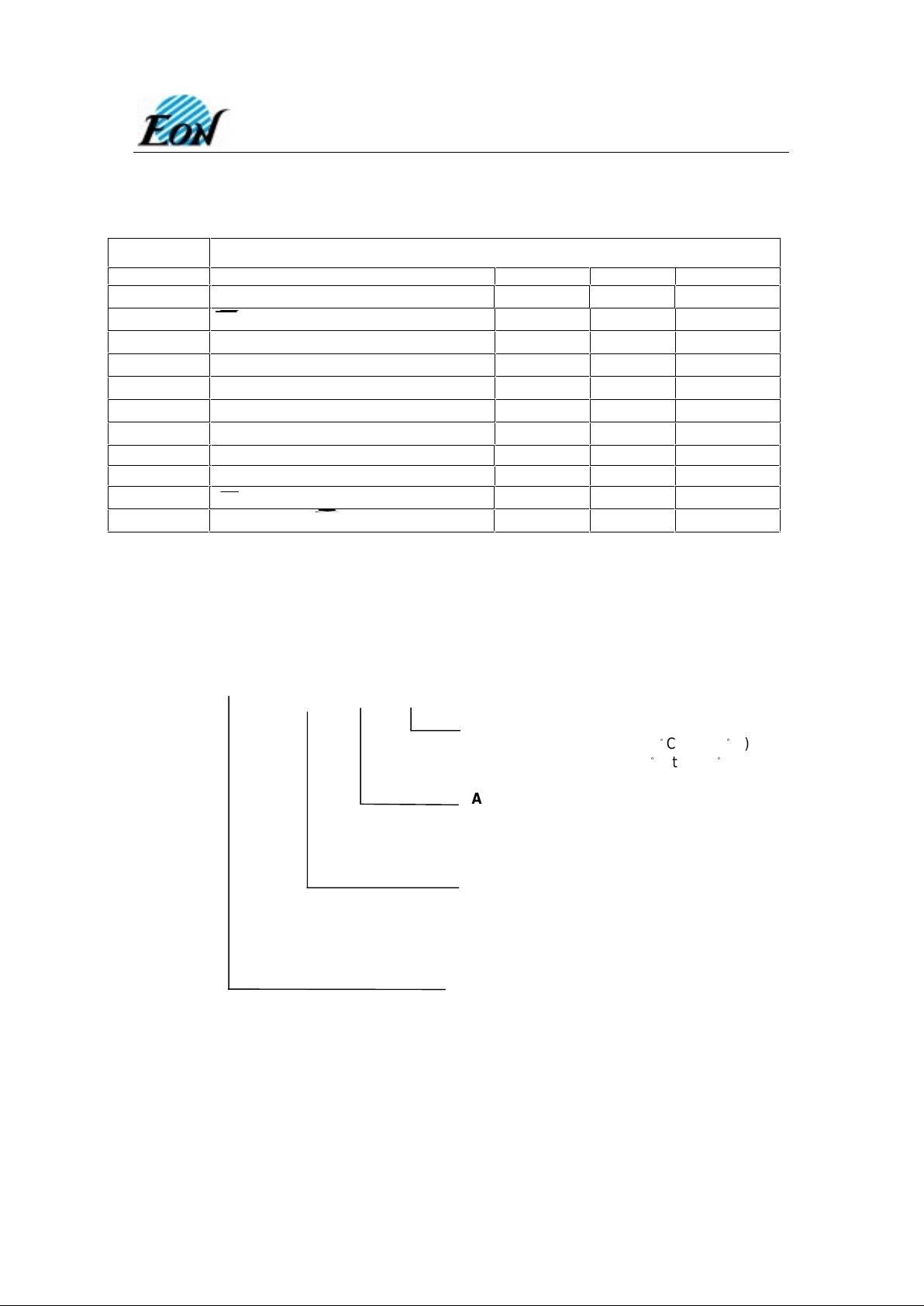
EN27C020
4800 Great America Parkway Ste 202 Tel: 408-235-8680
Santa Clara, CA. 95054 Fax: 408-235-8685
Preliminary
12
SWITCHING PROGRAMMING CHARACTERISTICS
(TΑ = + 25 ° C ± 5 ° C)
PARAMETER
SYMBOL
STANDARD PARAMETER DESCRIPTION
Min. Max Units
t
AS
Address Setup Time 2
µs
t
OES
OE Setup Time 2
µs
t
DS
Data Setup Time 2
µs
t
AH
Address Hold Time 0
µs
t
DH
Data Hold Time 2
µs
t
DFP
Output Enable to Output Float Delay 0 130 ns
t
VPS
VPP Setup Time 2
µs
t
PW
PGM Program Pulse Width
20
105
µs
t
VCS
V
cc
Setup Time 2
µs
t
CES
CE Setup Time
2
µs
t
OE
Data Valid from OE 150 ns
ORDERING INFORMATION
EN27C020 45 P I
TEMPERATURE RANGE
(Blank) = Commercial ( 0
Ý
C to +70ÝC)
I = Industrial ( -40
Ý
C to +85ÝC)
PACKAGE
P = 32 Plastic DIP
J = 32 Plastic PLCC
T = 32 Plastic TSOP
SPEED
45 = 45ns
55 = 55ns
70 = 70ns
90 = 90ns
BASE PART NUMBER
EN = EON Silicon Devices
27 = EPROM
C = CMOS
020 = 256K x 8
 Loading...