

Page 1

EN25T80
8 Mbit Uniform Sector, Serial Flash Memory with Dual Data Mode
EN25T80
FEATURES
• Single power supply operation
- Full voltage range: 2.7-3.6 volt
• 8 Mbit Serial Flash
- 8 M-bit/1024 K-byte/4096 pages
- 256 bytes per programmable page
• High performance
- 100MHz clock rate
- dual data mode
• Low power consumption
- 5 mA typical active current
- 1 μA typical power down current
• Uniform Sector Architecture:
- 256 sectors of 4-Kbyte
- 16 blocks of 64-Kbyte
- Any sector or block can be
erased individually
• Software and Hardware Write Protection:
GENERAL DESCRIPTION
- Write Protect all or portion of memory via
software
- Enable/Disable protection with WP# pin
• High performance program/erase speed
- Page program time: 1.5ms typical
- Sector erase time: 150ms typical
- Block erase time 800ms typical
- Chip erase time: 10 Seconds typical
• Lock ab le 256 by te OTP security sector
• Minimum 100K endurance cycle
• Package Options
- 8 pins SOP 200mil body width
- 8 pins PDIP
- 8 contact VDFN
- All Pb-free packages are RoHS compliant
• Commercial and industrial temperature
Range
The EN25T80 is a 8M-bit (1024K-byte) Serial Flash memory, with advanced write protection
mechanisms, accessed by a h igh spe ed SPI-compa tible bus. The memory c an be p rogramme d 1 to
256 bytes at a time, using the Page Program instruction.
The EN25T80 is designed to allow either single Sector at a time or full chip erase operation. The
EN25T80 can be configured to protect part of the memory as the software protected mode. The device
can sustain a minimum of 100K program/erase cycles on each sector.
This Data Sheet may be revised by subsequent versions ©2004 Eon Silicon Solution, Inc., www.essi.com.tw
or modifications due to changes in technical specifications.
Rev. A, Issue Date: 2006/11/6
1
Page 2
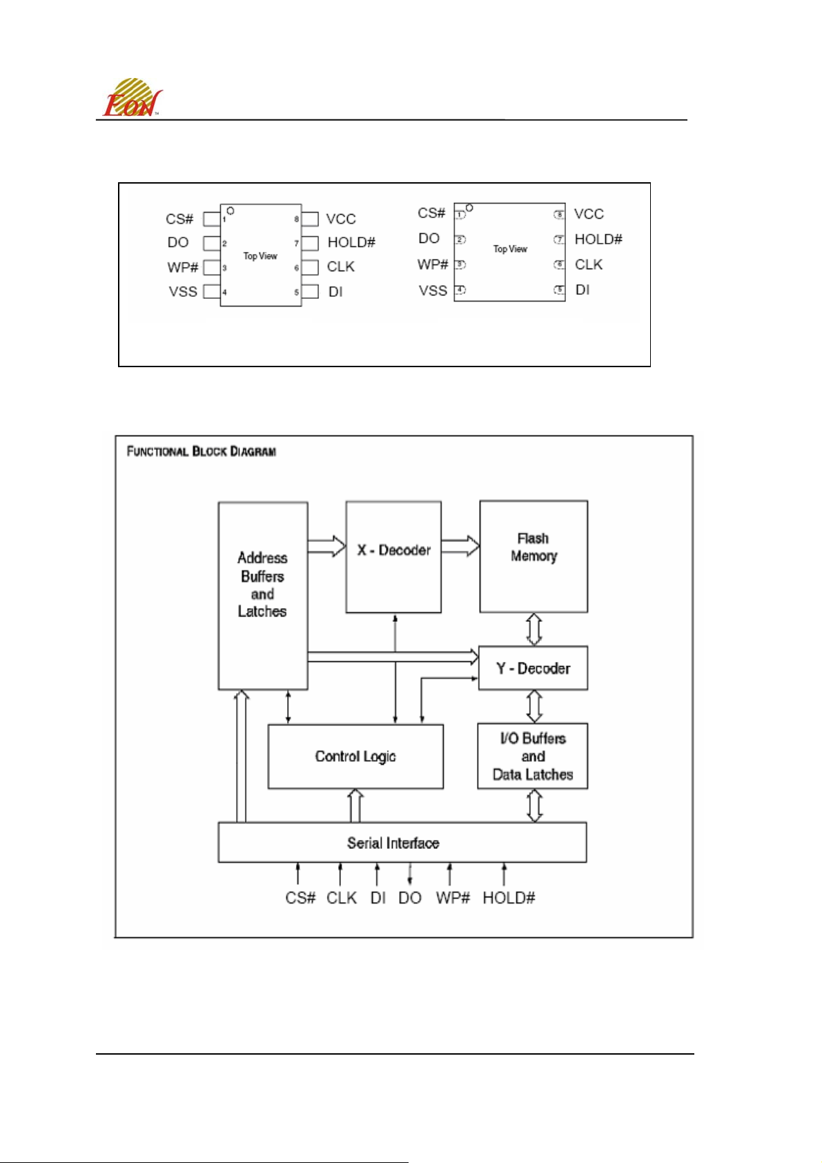
Figure.1 CONNECTION DIAGRAMS
8 - LEAD SOP 8 - CONTACT VDFN
Figure 2. BLOCK DIAGRAM
EN25T80
This Data Sheet may be revised by subsequent versions ©2004 Eon Silicon Solution, Inc., www.essi.com.tw
or modifications due to changes in technical specifications.
Rev. A, Issue Date: 2006/11/6
2
Page 3

EN25T80
SIGNAL DESCRIPTION
Serial Data Input (DI)
The SPI Serial Data Input (DI) pin provides a means for instructions, addresses and data to be
serially written to (shifted into) the device. Data is latched on the rising edge of the Serial Clock (CLK)
input pin.
Serial Data Output (DO)
The SPI Serial Data Output (DO) pin provides a means for data and status to be serially read from
(shifted out of) the device. Data is shifted out on the falling edge of the Serial Clock (CLK) input pin.
Serial Clock (CLK)
The SPI Serial Clock Input (CLK) pin provides the timing for serial input and output operations. ("See
SPI Mode")
Chip Select (CS#)
The SPI Chip Select (CS#) pin enables and disables device op eration . When CS# is hig h the device
is deselected and the Serial Data Output (DO) pin is at high impedance. When deselected, the
devices power consumption will be at standby levels unless an internal erase, program or status
register cycle is in progress. When CS# is brought low the device will be selected, power
consumption will increase to active levels and instructions can be written to and data read from the
device. After power-up, CS# must transition from high to low before a new instruction will be
accepted.
Hold (HOLD#)
The HOLD pin allows the device to be paused while it is actively selected. When HOLD is brought
low, while CS# is low, the DO pin will be at high impedance and signals on the DI and CLK pins will
be ignored (don’t care). The hold func tion can be us eful wh en multiple d evices a re sharin g th e s ame
SPI signals.
Write Protect (WP#)
The Write Protect (WP#) pin can be used to prevent the Status Register from bein g written. Use d
in conjunction with the Status Register’s Block Protect (BP0, BP1and BP2) bits and Status
Register Protect (SRP) bits, a portion or the entire memory array can be hardware protected.
Table 1. PIN Names
Symbol Pin Name
CLK Serial Clock Input
DI Serial Data Input
DO Serial Data Output
CS# Chip Enable
WP# Write Protect
HOLD# Hold Input
Vcc Supply Voltage (2.7-3.6V)
Vss Ground
This Data Sheet may be revised by subsequent versions ©2004 Eon Silicon Solution, Inc., www.essi.com.tw
or modifications due to changes in technical specifications.
Rev. A, Issue Date: 2006/11/6
3
Page 4

EN25T80
MEMORY ORGANIZATION
The memory is organized as:
z 1,048,576 bytes
z
Uniform Sector Architecture
16 blocks of 64-Kbyte
256 sectors of 4-Kbyte
z 4096 pages (256 bytes each)
Each page can be individually programmed (bits are programmed from 1 to 0). The device is Sector,
Block or Chip Erasable but not Page Erasable.
This Data Sheet may be revised by subsequent versions ©2004 Eon Silicon Solution, Inc., www.essi.com.tw
or modifications due to changes in technical specifications.
Rev. A, Issue Date: 2006/11/6
4
Page 5
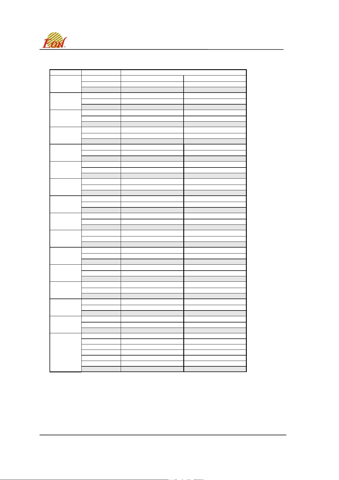
Table 2. Uniform Block Sector Architecture
Block Sector Address range
15
14
13
12
11
10
9
8
7
6
5
4
3
2
1
0
255 0FF000h 0FFFFFh
….
240 0F0000h 0F0FFFh
239 0EF000h 0EFFFFh
….
224 0E0000h 0E0FFFh
223 0DF000h 0DFFFFh
….
208 0D0000h 0D0FFFh
207 0CF000h 0CFFFFh
….
192 0C0000h 0C0FFFh
191 0BF000h 0BFFFFh
….
176 0B0000h 0B0FFFh
175 0AF000h 0AFFFFh
….
160 0A0000h 0A0FFFh
159 09F000h 09FFFFh
….
144 090000h 090FFFh
143 08F000h 08FFFFh
….
128 080000h 080FFFh
127 07F000h 07FFFFh
….
112 070000h 070FFFh
111 06F000h 06FFFFh
….
96 060000h 060FFFh
95 05F000h 05FFFFh
….
80 050000h 050FFFh
79 04F000h 04FFFFh
….
64 040000h 040FFFh
63 03F000h 03FFFFh
….
48 030000h 030FFFh
47 02F000h 02FFFFh
….
32 020000h 020FFFh
31 01F000h 01FFFFh
….
16 010000h 010FFFh
15 00F000h 00FFFFh
….
4 004000h 004FFFh
3 003000h 003FFFh
2 002000h 002FFFh
1 001000h 001FFFh
0 000000h 000FFFh
….
….
….
….
….
….
….
….
….
….
….
….
….
….
….
….
….
….
….
….
….
….
….
….
….
….
….
….
….
….
….
….
EN25T80
This Data Sheet may be revised by subsequent versions ©2004 Eon Silicon Solution, Inc., www.essi.com.tw
or modifications due to changes in technical specifications.
Rev. A, Issue Date: 2006/11/6
5
Page 6
EN25T80
OPERATING FEATURES
SPI Modes
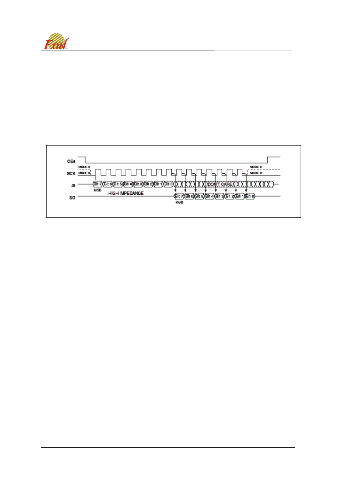
The EN25T80 is accessed through an SPI compatible bus consisting of four signals: Serial Clock (CLK),
Chip Select (CS#), Serial Data Input (DI) and Serial Data Output (DO). Both SPI bus operation Modes 0
(0,0) and 3 (1,1) are supported. The primary difference between Mode 0 and Mode 3, as shown in Figure
3, concerns the normal state of the SCK signal when the SPI bus master is in standby and data is not
being transferred to the Serial Flash. For Mode 0 the SCK signal is normally low. For Mode 3 the SCK
signal is normally high. In either case data input on the DI pin is sampled on th e rising edge of the SCK.
Data output on the DO pin is clocked out on the falling edge of SCK.
Figure 3. SPI Modes
Page Programming
To program one data byte, two instructions are required: Write Enable (WREN), which is one byte, and a
Page Program (PP) sequence, which consists of four bytes plus data. This is followed by the internal
Program cycle (of duration tPP).
To spread this overhead, the Page Program (PP) instruction allows up to 256 bytes to be programmed at
a time (changing bits from 1 to 0), provided that they lie in consecutive addresses on the same page of
memory.
Sector Erase, Block Erase and Chip Erase
The Page Program (PP) instruction allows bits to be reset from 1 to 0. Before this can be applied, the
bytes of memory need to have been erased to all 1s (FFh). This can be achieved a sector at a time, using
the Sector Erase (SE) instruction, a block at a time using the Block Erase (BE) instruction or throughout
the entire memory, using the Chip Erase (CE) instruction. This starts an internal Erase cycle (of duration
tSE tBE or tCE). The Erase instruction must be preceded by a Write Enable (WREN) instruction.
Polling During a Write, Program or Erase Cycle
A further improvement in the time to Write Status Register (WRSR), Program (PP) or Erase (SE, BE or
CE ) can be achieved by not waiting for the worst case delay (tW, tPP, tSE, tBEor tCE). The Write In
Progress (WIP) bit is provided in the Status Register so that the application program can monitor its value,
polling it to establish when the previous Write cycle, Program cycle or Erase cycle is complete.
Active Power, Stand-by Power and Deep Power-Down Modes
When Chip Select (CS#) is Low, the device is enabled, and in the Active Power mode. When Chip Select
(CS#) is High, the device is disabled, but could remain in the Active Power mode until all internal cycles
have completed (Program, Erase, Write Status Register). The device then goes into the Stand-by Power
mode. The device consumption drops to
I
CC1
.
The Deep Power-down mode is entered when the specific instruction (the Enter Deep Power-down Mode
(DP) instruction) is executed. The device consumption dr ops further to
I
. The device remains in this
CC2
mode until another specific instruction (the Release from Deep Power-down Mode and Read Device ID
(RDI) instruction) is executed.
All other instructions are ignored while the device is in the Deep Power-down mode. This can be used as
an extra software protection mechanism , when the device is not in active use, to protect the device from
inadvertent Write, Program or Erase instructions.
This Data Sheet may be revised by subsequent versions ©2004 Eon Silicon Solution, Inc., www.essi.com.tw
or modifications due to changes in technical specifications.
Rev. A, Issue Date: 2006/11/6
6
Page 7

Status Register. The Status Register contains a number of status and control bits that can be read or set
(as appropriate) by specific instructions.
WIP bit. The Write In Progress (WIP) bit indicates whether the memory is busy with a Write Status
Register, Program or Erase cycle.
WEL bit. The Write Enable Latch (WEL) bit indicates the status of the internal Write Enable Latch.
BP2, BP1, BP0 bits. The Block Protect (BP2, BP1, BP0) bits are non-volatile. They define the size of the
area to be software protected against Program and Erase instructions.
Mode1, Mode0 bits. Default value is SPI mode (00), user can change this value by change mode
commands to change the interface mode. This device also support SP2 mode (01).
SP2 mode : command/address/data all transmitting with 2 bits
SRP bit /
Protect (WP#) signal. The Status Register Protect (SRP) bit and Write Protect (WP#) signal allow the
device to be put in the Hardware Protected mode. In this mode, the non-volatile bits of the Stat us Reg ister
(SRP, BP2, BP1, BP0) become read-only bits.
In OTP mode, this bit is served as OTP_LOCK bit, user can read/program/erase OTP sector as normal
sector while OTP_LOCK value is equal 0, after OTP_LOCK is programmed with 1 by WRSR command,
the OTP sector is protected from program and erase operation. The OTP_LOCK bit can only be
programmed once.
Note : In OTP mode, the WRSR command will ignore any input data and program OTP_LOCK bit to 1, user
must clear the protect bits before enter OTP mode and program the OTP code, then execute WRSR command
to lock the OTP sector before leaving OTP mode.
Write Protection
Applications that use non-volatile memory must take into consideration the possibility of noise and other
adverse system conditions that may compromise data integrity. To address this concern the EN25T80
provides the following data protection mechanisms:
z Power-On Reset and an internal timer (t
z Program, Erase and Write Status Register instructions are checked that they consist of a number of
OTP_LOCK bit The Status Register Protect (SRP) bit is operated in conjunction with the Write
) can provide protection against inadvertent changes
PUW
while the power supply is outside the operating specification.
clock pulses that is a multiple of eight, before they are accepted for execution.
EN25T80
z All instructions that modify data must be preceded by a Write Enable (WREN) instruction to set the
Write Enable Latch (WEL) bit . This bit is returned to its reset state by the following events:
– Power-up
– Write Disable (WRDI) instruction completion or Write Status Register (WRSR) instruction
completion or Page Program (PP) instruction completion or Sector Erase (SE)instruction
completion or Block Erase (BE) instruction completion or Chip Erase (CE) instruction completion
z The Block Protect (BP2, BP1, BP0) bits allow part of the memory to be configur ed as read-only. This
is the Software Protected Mode (SPM).
z The Write Protect (WP#) signal allows the Block Protect (BP2, BP1, BP0) bits and Status Register
Protect (SRP) bit to be protected. This is the Hardware Protected Mode (HPM).
z In addition to the low power consumption feature, the Deep Power-down mode offers extra software
protection from inadvertent Write, Program and Erase instructions, as all instructions are ignored
except one particular instruction (the Release from Deep Power-down instruction).
This Data Sheet may be revised by subsequent versions ©2004 Eon Silicon Solution, Inc., www.essi.com.tw
or modifications due to changes in technical specifications.
Rev. A, Issue Date: 2006/11/6
7
Page 8
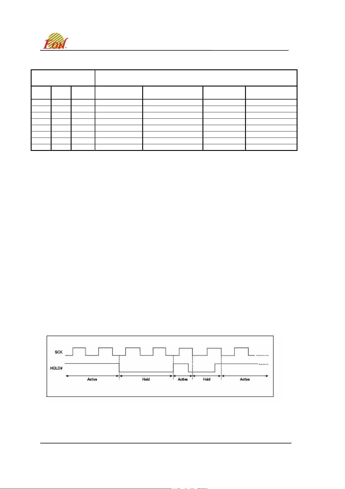
TABLE 3. Protected Area Sizes Sector Organization
EN25T80
Status Register
Content
BP2
Bit
1 1 1 All 000000h-0FFFFFh 1024KB All
1 1 0 All 000000h-0FFFFFh 1024KB All
1 0 1 All 000000h-0FFFFFh 1024KB All
1 0 0 8 to 15 080000h-0FFFFFh 512KB Upper 1/2
0 1 1 12 to 15 0C0000h-0FFFFFh 256KB Upper 1/4
0 1 0 14 to 15 0E0000h-0FFFFFh 128KB Upper 1/8
0 0 1 15 0F0000h-0FFFFFh 64KB Upper 1/16
0 0 0 None None None None
BP1
Bit
BP0
Bit
Protect Blocks
Memory Content
Addresses
Density(KB)
Portion
Hold Function
The Hold (HOLD) signal is used to pause any serial communications with the device without resetting the
clocking sequence. However, taking this signal Low does not terminate any Write Status Register,
Program or Erase cycle that is currently in progress.
To enter the Hold condition, the device must be selected, with Chip Select (CS#) Low. The Hold condition
starts on the falling edge of the Hold (HOLD) signal, provided that this coincides with Serial Clock (CLK)
being Low (as shown in Figure 4.).
The Hold condition ends on the rising edge of the Hold (HOLD) signal, provided that this coincides with
Serial Clock (CLK) being Low.
If the falling edge does not coincide with Serial Clock (CLK) being Low, the Hold condition starts after
Serial Clock (CLK) next goes Low. Similarly, if the rising edge does not coincide with Serial Clock (CLK)
being Low, the Hold condition ends after Serial Clock (CLK) next goes Low. (This is shown in Figure 4.).
During the Hold condition, the Serial Data Output (DO) is high impedance, and Serial Data Input (DI) and
Serial Clock (CLK) are Don’t Care.
Normally, the device is kept selected, with Chip Select (CS#) driven Low, for the whole duration of the
Hold condition. This is to ensure that the state of the internal logic remains unchanged from the moment
of entering the Hold condition.
If Chip Select (CS#) goes High while the device is in the Hold condition, this has the effect of resetting the
internal logic of the device. To restart communication with the device, it is necessary to drive Hold (HOLD)
High, and then to drive Chip Select (CS#) Low. This prevents the device from going back to the Hold
condition.
Figure 4. Hold Condition Waveform
This Data Sheet may be revised by subsequent versions ©2004 Eon Silicon Solution, Inc., www.essi.com.tw
or modifications due to changes in technical specifications.
Rev. A, Issue Date: 2006/11/6
8
Page 9
EN25T80
INSTRUCTIONS
All instructions, addresses and data are shifted in and out of the device, most significant bit first. Serial
Data Input (DI) is sampled on the first rising edge of Serial Clock (C LK ) after Chip Select (CS#) is driven
Low. Then, the one-byte instruction code must be shifted in to the device, most significant bit first, on
Serial Data Input (DI), each bit being latched on the rising edges of Serial Clock (CLK).
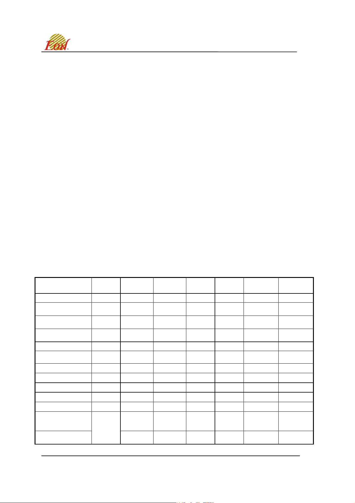
The instruction set is listed in Table 4. Every instruction sequence starts with a one-byte instruction code.
Depending on the instruction, this might be followed by address bytes, or by data bytes, or by both or
none. Chip Select (CS#) must be driven High after the last bit of the instruction sequence has been shifted
in. In the case of a Read Data Bytes (READ), Read Data Bytes at Higher Speed (Fast_Read), Read
Status Register (RDSR) or Release from Deep Power-down, and Read Device ID (RDI) instruction, the
shifted-in instruction sequence is followed by a data-out sequence. Chip Select (CS#) can be driven High
after any bit of the data-out sequence is being shifted out.
In the case of a Page Program (PP), Secto r Erase (SE), Blo ck Erase ( BE), Chip Erase (CE) , Write Status
Register (WRSR), Write Enable (WREN), Write Disable (WRDI) or Deep Power-down (DP) instruction,
Chip Select (CS#) must be driven High exactly at a byte boundary, otherwise the instruction is rejected,
and is not executed. That is, Chip Select (CS#) must driven High when the number of clock pulses after
Chip Select (CS#) being driven Low is an exact multiple of eight. For Page Program, if at any time the
input byte is not a full byte, nothing will happen and WEL will not be reset.
In the case of multi-byte commands of Page Program (PP), and Release from Deep Power Down
(RES ) minimum number of bytes specified has to be given, without w hich, the command w ill be
ignored.
In the case of Page Program, if the number of byte after the command is less than 4 (at least 1 data
byte), it will be ignored too. In the case of SE and BE, exact 24-bit address is a must, any less or
more will cause the command to be ignored.
All attempts to access the memory array during a Write Status Register cycle, Program cycle or Erase
cycle are ignored, and the internal Write Status Register cycle, Program cycle or Erase cycle continues
unaffected.
Table 4. Instruction Set
Instruction Name Byte 1
Code
Write Enable 06h
Write Disable / Exit
EXT / OTP mode
Read Status
Register
Write Status
Register
04h
05h
01h
Read Data 03h
Fast Read 0Bh
Page Program 02h
Sector Erase 20h
Block Erase D8h/ 52h
Chip Erase C7h/ 60h
Deep Power-down B9h
Release from Deep
Power-down, and
read Device ID
ABh
Release from Deep
Power-down
Byte 2 Byte 3 Byte 4 Byte 5 Byte 6 n-Bytes
continuous
(S7-S0)
S7-S0
A23-A16 A15-A8 A7-A0 (D7-D0) (Next byte)
A23-A16 A15-A8 A7-A0 dummy (D7-D0)
A23-A16 A15-A8 A7-A0 D7-D0 (Next byte) continuous
A23-A16 A15-A8 A7-A0
A23-A16 A15-A8 A7-A0
dummy dummy dummy (ID7-ID0)
(1)
(4)
(2)
continuous
(Next Byte)
continuous
This Data Sheet may be revised by subsequent versions ©2004 Eon Silicon Solution, Inc., www.essi.com.tw
or modifications due to changes in technical specifications.
Rev. A, Issue Date: 2006/11/6
9
Page 10
Manufacturer/
90h
Device ID
Read Identification 9Fh
dummy dummy
(M7-M0)
(ID15-ID8) (ID7-ID0)
00h
(5)
(M7-M0) (ID7-ID0)
EN25T80
Enter EXT mode 0Ah
Enter OTP mode 3Ah
Notes:
1. Data bytes are shifted with Most Significant Bit first. Byte fields with data in parenthesis “( )” indicate data being read from
the device on the DO pin.
2. The Status Register contents will repeat continuously until CS# terminate the instruction.
3. All sectors may use any address within the sector.
4. The Device ID will repeat continuously until CS# terminate the instruction.
5. The Manufacturer ID and Device ID bytes will repeat continuously until CS# terminate the instruction.
00h on Byte 4 starts with MID and alternate with DID, 01h on Byte 4 starts with DID and alternate with MID.
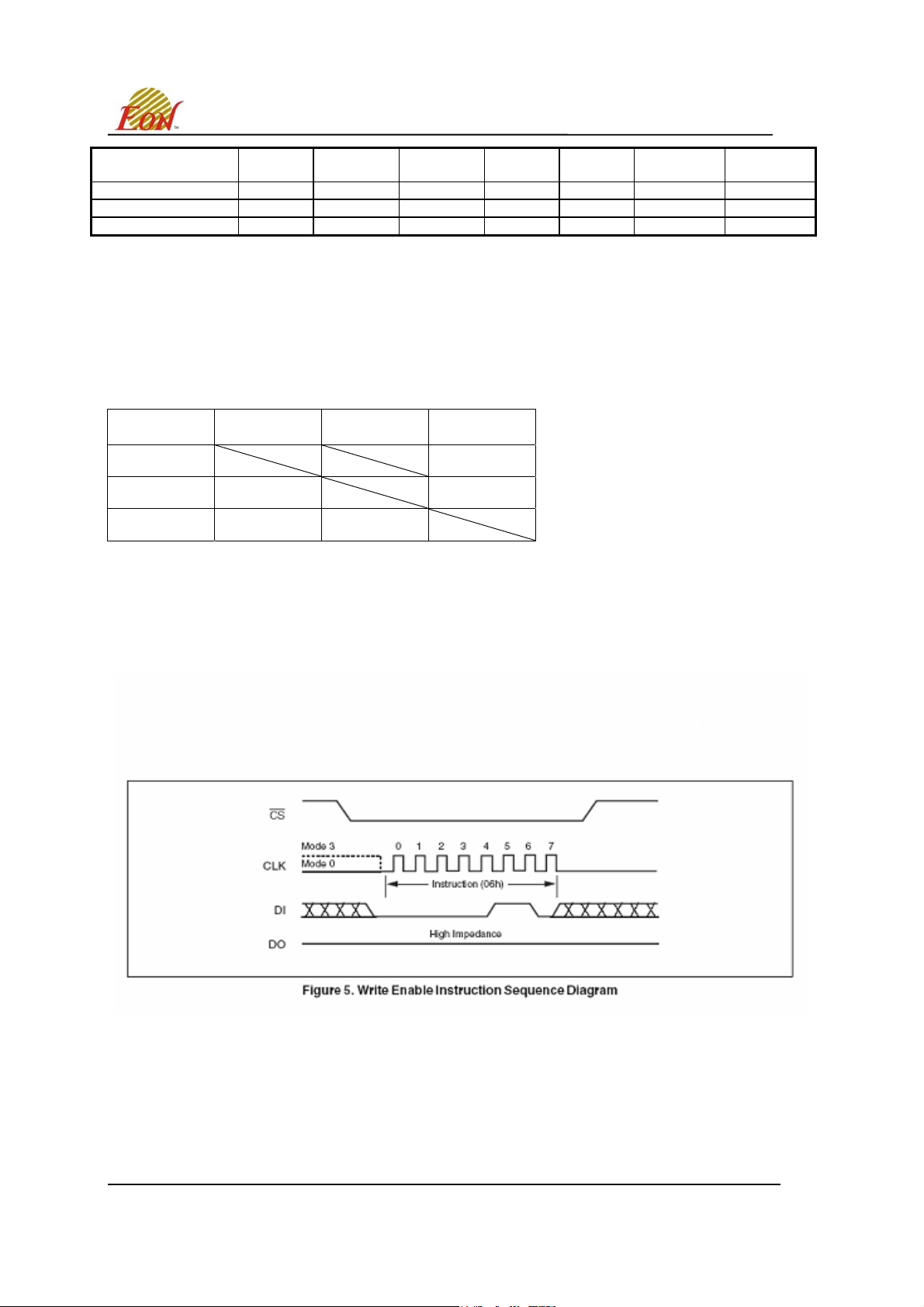
Table 5. Manufacturer and Device Identification
OP Code (M7-M0) (ID15-ID0) (ID7-ID0)
ABh 13h
90h 1Ch 13h
9Fh 1Ch 5114h
Write Enable (WREN) (06h)
The Write Enable (WREN) instruction (Figure 5)
sets the Write Enable Latch (WEL) bit. The Write Enable
Latch (WEL) bit must be set prior to every Page Program (PP), Sector Erase (SE), Block Erase (BE), Chip
Erase (CE) and Write Status Register (WRSR) instruction.
The Write Enable (WREN) instruction is entered by driving Chip Select (CS#) Low, sending the instruction
code, and then driving Chip Select (CS#) High.
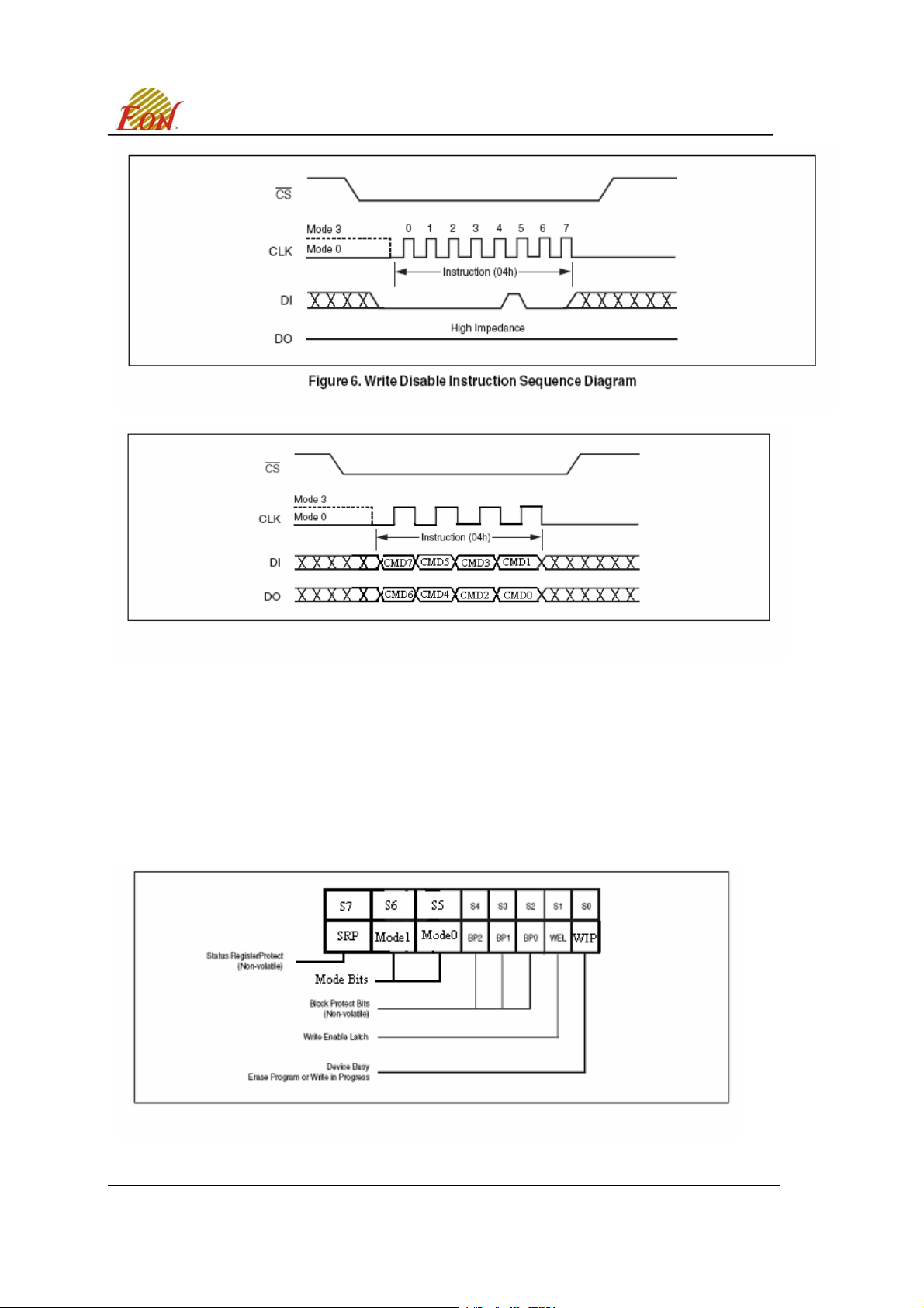
Write Disable (WRDI) (04h)
The Write Disable instruction (Figure 6) resets the Write Enable Latch (WEL) bit in the Status Register to
a 0 or exit from EXT / OTP mode to normal mode. The Write Disable instruction is entered by driving Chip
Select (CS#) low, shifting the instruction code “04h” into the DI pin and then driving Chip Select (CS#)
high. Note that the WEL bit is automatically reset after Power-up and upon completion of the Write Status
Register, Page Program, Sector Erase, Block Erase (BE) and Chip Erase instructions.
This Data Sheet may be revised by subsequent versions ©2004 Eon Silicon Solution, Inc., www.essi.com.tw
or modifications due to changes in technical specifications.
Rev. A, Issue Date: 2006/11/6
10
Page 11
EN25T80
Figure 6.1 Write Disable Instruction Sequence Diagram of SP2 Mode
Read Status Register (RDSR) (05h)
The Read Status Register (RDSR) instruction allows the Status Register to be read. The Status Register
may be read at any time, even while a Program, Erase or Write Status Register cycle is in progress.
When one of these cycles is in progress, it is recommended to check the Write In Progress (WIP) bit
before sending a new instruction to the device. It is also possible to read th e Status Register co ntinuously,
as shown in Figure 7.
Table 6. Status Register Bit Locations
Note :
In OTP mode, SRP bit is served as OTP_LOCK bit.
This Data Sheet may be revised by subsequent versions ©2004 Eon Silicon Solution, Inc., www.essi.com.tw
or modifications due to changes in technical specifications.
Rev. A, Issue Date: 2006/11/6
11
Page 12
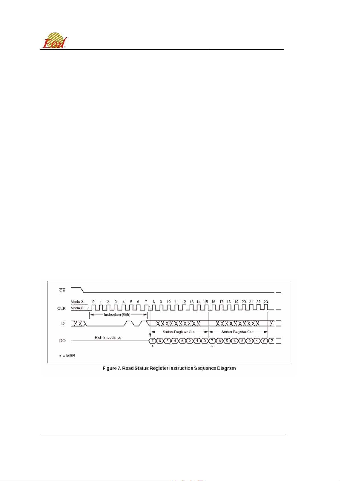
The status and control bits of the Status Register are as follows:
WIP bit. The Write In Progress (WIP) bit indicates whether the memory is busy with a Write Status
Register, Program or Erase cycle. When set to 1, such a cycle is in progress, when reset to 0 no such
cycle is in progress.
WEL bit. The Write Enable Latch (WEL) bit indicates the status of the internal Write Enable Latch. When
set to 1 the internal Write Enable Latch is set, when set to 0 the internal Write Enable Latch is reset and
no Write Status Register, Program or Erase instruction is accepted.
EN25T80
BP2, BP1, BP0 bits. The Block Protect (BP2, BP1, BP0) bits are non-volatile. They define the size of the
area to be software protected against Program and Erase instructions. These bits are written with the
Write Status Register (WRSR) instruction. When one or both of the Block Protect (BP2, BP1, BP0) bits is
set to 1, the relevant memory area (as defined in Table 3.) becomes protected against Page Program (PP)
Sector Erase (SE) and , Block Erase (BE), instruct ions. The Block Protect (BP2, BP1, BP0) bits can be
written provided that the Hardware Protected mode ha s not been set. The Chip Era se (CE) instruction is
executed if, and only if, both Block Protect (BP2, BP1, BP0) bits are 0.
Mode1, Mode0 bits. Default value is SPI mode (00), user can change this value by change mode
commands to change the interface mode. This device also support SP2 mode (01).
SRP bit / OTP_LOCK bit. The Status Register Protect (SRP) bit is operated in conjunction with the Write
Protect (WP#) signal. The Status Register Write Protect (SRP) bit and Write Protect (WP#) signal allow
the device to be put in the Hardware Protected mode (when the Status Register Protect (SRP) bit is set to
1, and Write Protect (WP#) is driven Low). In this mode, the non-volatile bits of the Status Register (SRP,
BP2, BP1, BP0) become read-only bit s and the Write Status Register (WRSR) instruction is no long er
accepted for execution.
In OTP mode, this bit is served as OTP_LOCK bit, user can read/program/erase OTP sector as normal
sector while OTP_LOCK value is equal 0, after OTP_LO CK is programmed with 1 by WRSR command,
the OTP sector is protected from program and erase operation. The OTP_LOCK bit can only be
programmed once.
Note : In OTP mode, the WRSR command will ignore any input data and program OTP_LOCK bit to 1, user
must clear the protect bits before enter OTP mode and program the OTP code, then execute WRSR command
to lock the OTP sector before leaving OTP mode.
This Data Sheet may be revised by subsequent versions ©2004 Eon Silicon Solution, Inc., www.essi.com.tw
or modifications due to changes in technical specifications.
Rev. A, Issue Date: 2006/11/6
12
Page 13
EN25T80
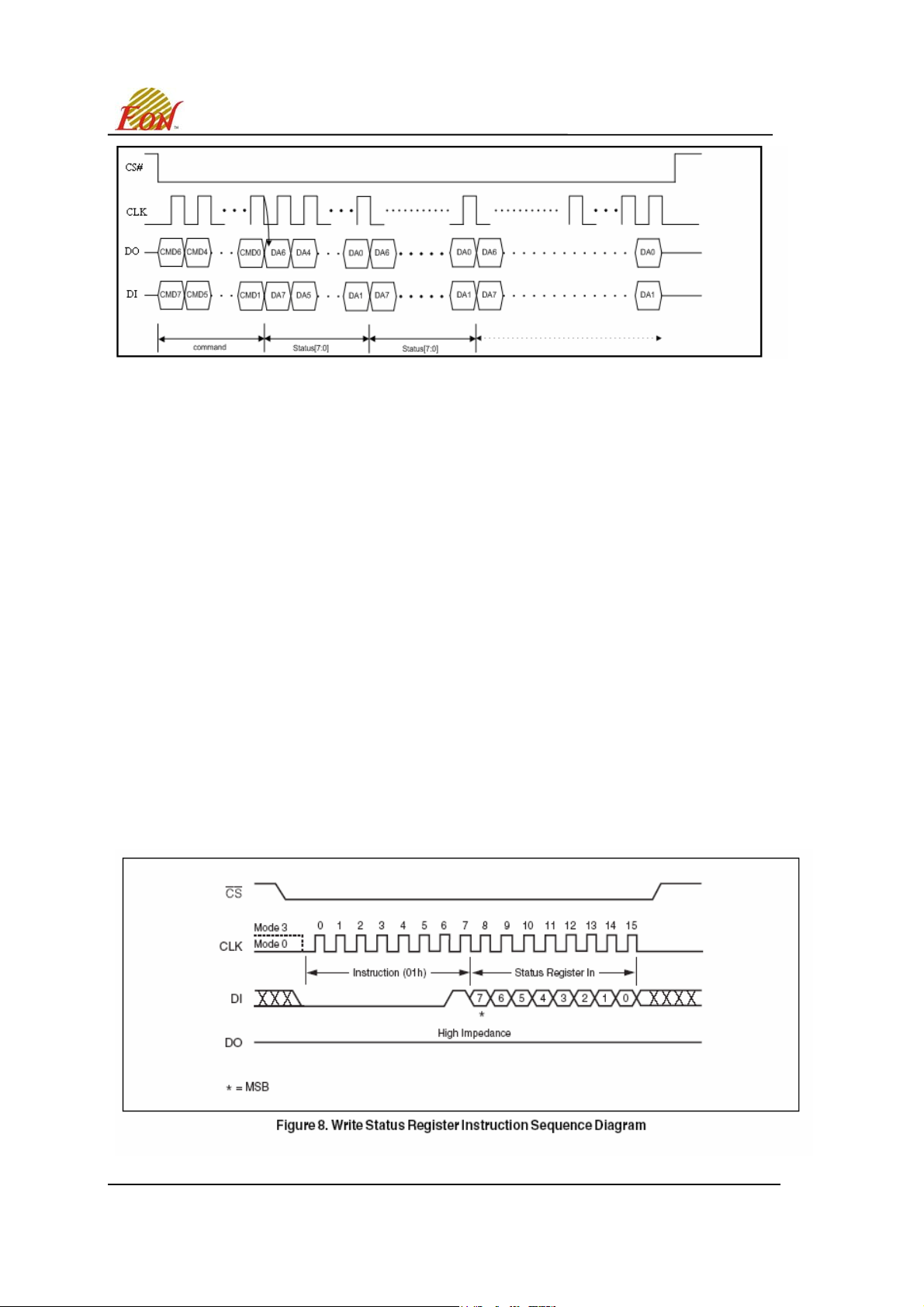
Figure 7.1 Read Status Register Instruction Sequence Diagram of SP2 Mode
Write Status Register (WRSR) (01h)
The Write Status Register (WRSR) instruction allows new values to be written to the Status Register.
Before it can be accepted, a Write Enable (WREN) instruction must previously have been executed. After
the Write Enable (WREN) instruction has been decoded and executed, the device sets the Write Enable
Latch (WEL).
The Write Status Register (WRSR) instruction is entered by driving Chip Select (CS#) Low, followed by
the instruction code and the data byte on Serial Data Input (DI).
The instruction sequence is shown in Figure 8.. The Write Status Register (WRSR) instruction has no
effect on S6, S5, S1 and S0 of the Status Register. S6 and S5 are always read as 0. Chip Select (CS#)
must be driven High after the eighth bit of the data byte has been latched in. If not, the Write Status
Register (WRSR) instruction is not executed. As soon as Chip Select (CS#) is driven High, the self-timed
Write Status Register cycle (whose duration is tW) is initiated. While the Write Status Register cycle is in
progress, the Status Register may still be read to check the value of the Write In Progress (WIP) bit. The
Write In Progress (WIP) bit is 1 during the self-timed Write Status Register cycle, and is 0 when it is
completed. When the cycle is completed, the Write Enable Latch (WEL) is reset.
The Write Status Register (WRSR) instruction allows the user to change the values of the Block Protect
(BP2, BP1, BP0) bits, to define the size of the area that is to be treated as read-only, as defined in Table
3.. The Write Status Register (WRSR) instruction also allows the user to set or reset the Status Register
Protect (SRP) bit in accordance with the Write Protect (WP#) signal. The Status Register Protect (SRP)
bit and Write Protect (WP#) signal allow the device to be put in the Hardware Protected Mode (HPM). The
Write Status Register (WRSR) instruction is not executed once the Hardware Protected Mode (HPM) is
entered.
NOTE : In the OTP mode, WRSR command will ignore input data and program OTP_LOCK bit to 1.
This Data Sheet may be revised by subsequent versions ©2004 Eon Silicon Solution, Inc., www.essi.com.tw
or modifications due to changes in technical specifications.
Rev. A, Issue Date: 2006/11/6
13
Page 14
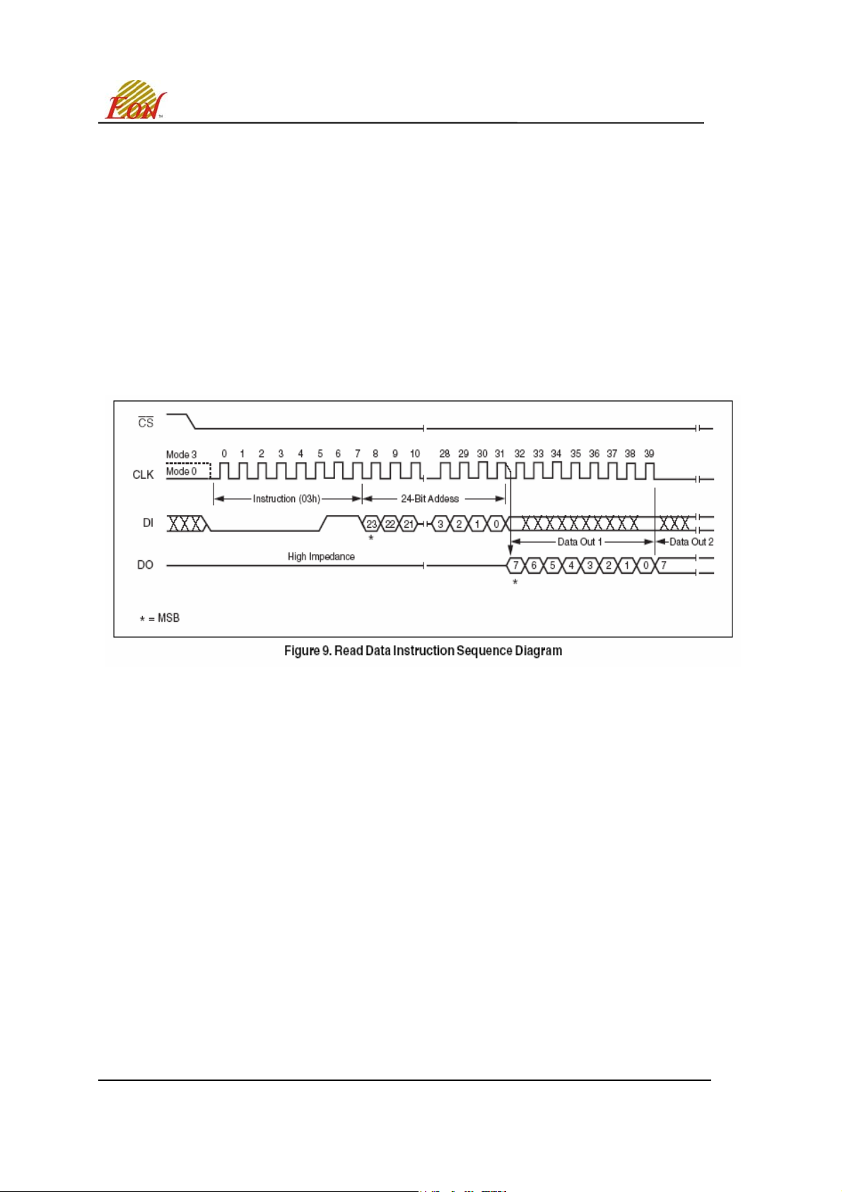
Read Data Bytes (READ) (03h)
The device is first selected by driving Chip Select (CS#) Low. The instruction code for the Read Data
Bytes (READ) instruction is followed by a 3-byte address (A23-A0), each bit being latched-in during the
rising edge of Serial Clock (CLK). Then the memory contents, at that address, is shifted out on Serial Data
Output (DO), each bit being
(CLK).
The instruction sequence is shown in Figure 9.. The first byte addressed can be at any location. The
address is automatically incremented to the next higher address after each byte of data is shifted out. The
whole memory can, therefore, be read with a single Read Data Bytes (READ) instruction. When the
highest address is reached, the address counter rolls over to 000000h, allowing the read sequence to be
continued indefinitely.
The Read Data Bytes (READ) instruction is terminated by driving Chip Select (CS#) High. Chip Se lect
(CS#) can be driven High at any time during data ou tput. Any Read Data Bytes (READ) instruction, while
an Erase, Program or Write cycle is in progress, is rejected without having any effects on the cycle that is
in progress.
shifted out, at a maximum frequency fR, during the falling edge of Serial Clock
EN25T80
Read Data Bytes at Higher Speed (FAST_READ) (0Bh)
The device is first selected by driving Chip Select (CS#) Low. The instruction code for the Read Data
Bytes at Higher Speed (FAST_READ) instruction is followed by a 3-byte address (A23-A0) and a dummy
byte, each bit being latched-in during the rising edge of Serial Clock (CLK). Then the memory contents, at
that address, is shifted out on Serial Data Output (DO), each bit being shifted out, at a maximum
frequency F
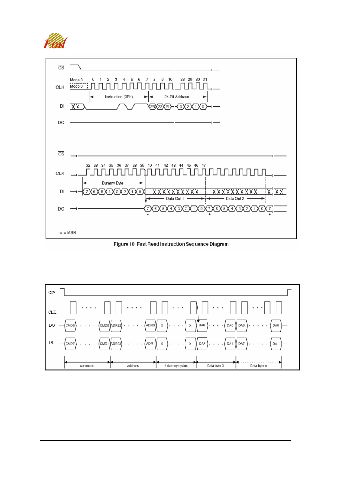
The instruction sequence is shown in Figure 10 and Figure 10.1 for SPI mode and SP2 mode. The first
byte addressed can be at any location. The address is automatically incremented to the next higher
address after each byte of data is shifted out. The whole memory can, therefore, be read with a single
Read Data Bytes at Higher Speed (FAST_READ) instruction. When the highest address is reached, the
address counter rolls over to 000000h, allowing the read sequence to be continued inde finit ely.
The Read Data Bytes at Higher Speed (FAST_READ) instruction is terminated by driving Chip Select
(CS#) High. Chip Select (CS#) can be driven High a t any time during data output. Any Read Data Bytes at
Higher Speed (FAST_READ) instruction, while an Erase, Program or Write cycle is in progress, is
rejected without having any effects on the cycle that is in progress.
Notes : The number of dummy cycles in SPI and SP2 mode are eight and four.
, during the falling edge of Serial Clock (CLK).
R
This Data Sheet may be revised by subsequent versions ©2004 Eon Silicon Solution, Inc., www.essi.com.tw
or modifications due to changes in technical specifications.
Rev. A, Issue Date: 2006/11/6
14
Page 15
EN25T80
Figure 10.1 Fast Read Instruction Sequence Diagram of SP2 Mode
This Data Sheet may be revised by subsequent versions ©2004 Eon Silicon Solution, Inc., www.essi.com.tw
or modifications due to changes in technical specifications.
Rev. A, Issue Date: 2006/11/6
15
Page 16
Page Program (PP) (02h)
The Page Program (PP) instruction allows bytes to be programmed in the memory. Before it can be
accepted, a Write Enable (WREN) instruction must previously have been executed. After the Write Enable
(WREN) instruction has been decoded, the device sets the Write Enable Latch (WEL).
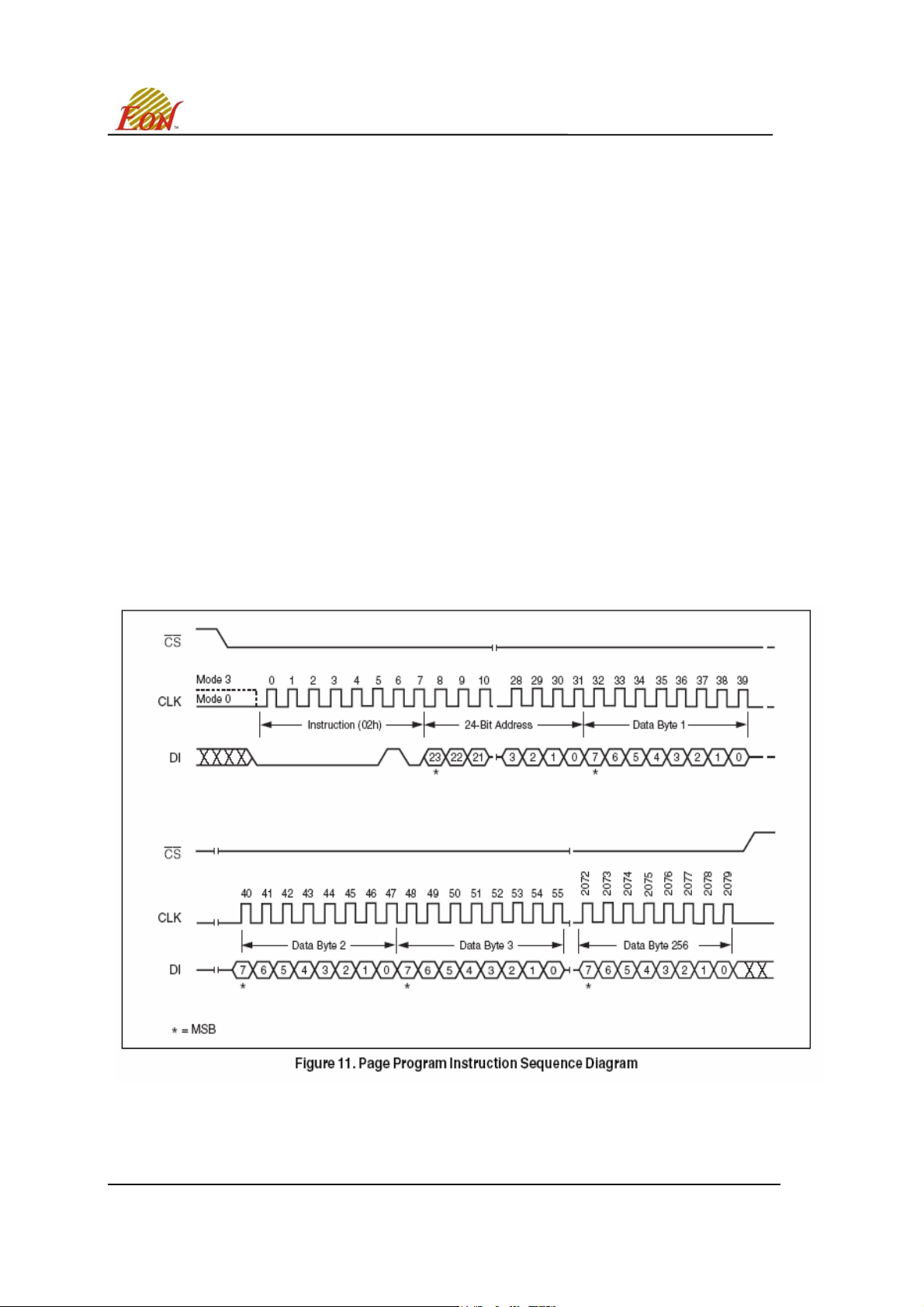
The Page Program (PP) instruction is entered by driving Chip Select (CS#) Low, followed by the instruction code, three address bytes and at least one data byte on Serial Data Input (DI). If the 8 least
significant address bits (A7-A0) are not all zero, all transmitted data that goes beyond the end of the
current page are programmed from the start address of the same page (from the address whose 8 least
significant bits (A7-A0) are all zero). Chip Select (CS#) must be driven Low for the entire duration of the
sequence.
The instruction sequence is shown in Figure 11. If more than 256 bytes are sent to the device, previously
latched data are discarded and the last 256 data bytes are guaranteed to be programmed correctly within
the same page. If less than 256 Data bytes are sent to device, they are correctly programmed at the
requested addresses without having any effects on the other bytes of the same page.
Chip Select (CS#) must be driven High after the eighth bit of the last data byte has been latched in,
otherwise the Page Program (PP) instruction is not executed.
As soon as Chip Select (CS#) is driven High, the self-timed Pa ge Pro gram cycle (whose dur atio n is t
initiated. While the Page Program cycle is in progress, the Status Register may be read to check the value
of the Write In Progress (WIP) bit. The Write In Progress (WIP) bit is 1 during the self-timed Page
Program cycle, and is 0 when it is completed. At some unspecified time before the cycle is completed, the
Write Enable Latch (WEL) bit is reset.
A Page Program (PP) instruction applied to a page which is protected by the Block Protect (BP2, BP1,
BP0) bits (see Table 3) is not executed.
EN25T80
PP) is
This Data Sheet may be revised by subsequent versions ©2004 Eon Silicon Solution, Inc., www.essi.com.tw
or modifications due to changes in technical specifications.
Rev. A, Issue Date: 2006/11/6
16
Page 17
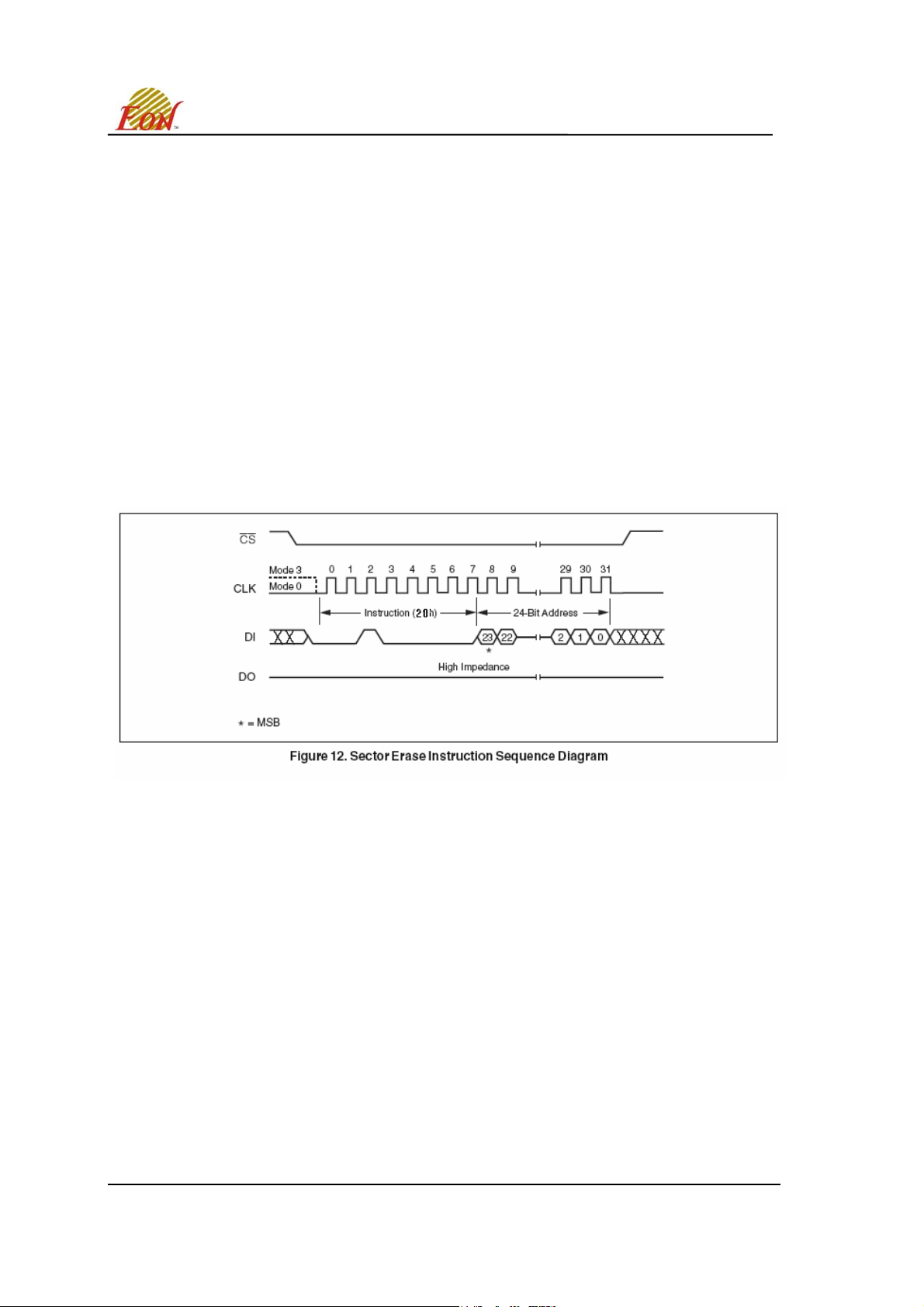
Sector Erase (SE) (20h)
The Sector Erase (SE) instruction sets to 1 (FFh) all bits inside the chosen sector. Before it can be
accepted, a Write Enable (WREN) instruction must previously have been executed. After the Write
Enable (WREN) instruction has been decoded, the device sets the Write Enable Latch (WEL).
The Sector Erase (SE) instruction is en tered by driving Chip Select (CS#) Low, followed by the instruction code, and three address bytes on Serial Data Input (DI). Any address inside the Sector (see
Table 2) is a valid address for the Sector Erase (SE) instruction. Chip Select (CS#) must be driven
Low for the entire duration of the sequence.
The instruction sequence is shown in Figure 12.. Chip Select (CS#) must be driven High after the eighth
bit of the last address byte has been latched in, otherwise the Sector Erase (SE) instruction is not
executed. As soon as Chip Select (CS#) is driven High, the self-timed Sector Erase cycle (whose duration
is t
SE
the value of the Write In Progress (WIP) bit. The Write In Progress (WIP) bit is 1 during the self-timed
Sector Erase cycle, and is 0 when it is completed. At some unspecified time before the cycle is completed,
the Write Enable Latch (WEL) bit is reset.
A Sector Erase (SE) instruction applied to a sector which is protected by the Block Protect (BP2, BP1,
BP0) bits (see Table 3) is not executed.
) is initiated. While the Sector Erase cycle is in progress, the Status Register may be read to check
EN25T80
Block Erase (BE) (D8h/52h)
The Block Erase (BE) instruction sets to 1 (FFh) all bits inside the chosen block. Before it can be
accepted, a Write Enable (WREN) instruction must previously have been executed. After the Write
Enable (WREN) instruction has been decoded, the device sets the Write Enable Latch (WEL).
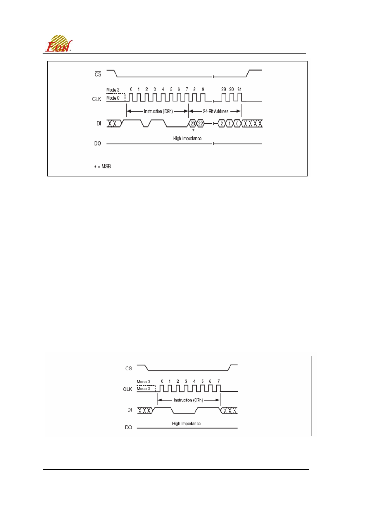
The Block Erase (BE) instruction is entered b y driving Chip Select (CS#) Low, followed by the instruction code, and three address bytes on Serial Data Input (DI). Any address inside the Block (see
Table 2) is a valid address for the Block Erase (BE) instruction. Chip Select (CS#) must be driven
Low for the entire duration of the sequence.
The instruction sequence is shown in Figure 13.. Chip Select (CS#) must be driven High after the eighth
bit of the last address byte has been latched in, otherwise the Block Erase (BE) instruction is not executed.
As soon as Chip Select (CS#) is driven High, the self-timed Block Erase cycle (whose duration is t
initiated. While the Block Erase cycle is in progress, the Status Register may be read to check the value of
the Write In Progress (WIP) bit. The Write In Progress (WIP) bit is 1 during the self-timed Block Erase
cycle, and is 0 when it is completed. At some unspecified time before the cycle is completed, the Write
Enable Latch (WEL) bit is reset.
A Block Erase (BE) instruction applied to a block which is protected by the Block Protect (BP2, BP1, BP0)
bits (see Table 3) is not executed.
SE
) is
This Data Sheet may be revised by subsequent versions ©2004 Eon Silicon Solution, Inc., www.essi.com.tw
or modifications due to changes in technical specifications.
Rev. A, Issue Date: 2006/11/6
17
Page 18
EN25T80
Figure 13 Block Erase Instruction Sequence Diagram
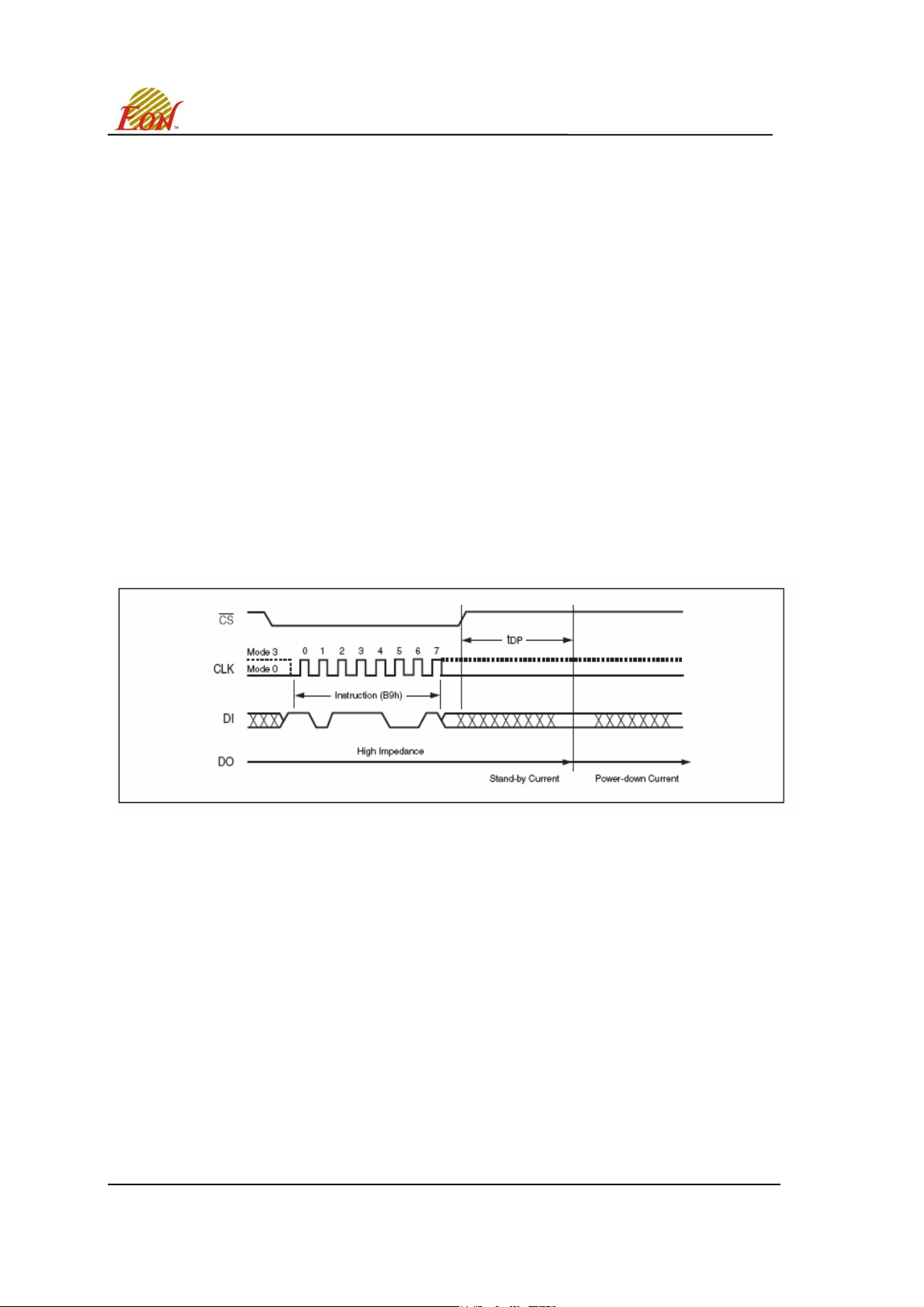
Chip Erase (CE) (C7h/60h)
The Chip Erase (CE) instruction sets all bits to 1 (FFh). Before it can be accepted, a Write Enable
(WREN) instruction must previously have been executed. After the Write Enable (WREN) instruction
has been decoded, the device sets the Write Enable Latch (WEL).
The Chip Erase (CE) instruction is entered by driving Chip Select (CS#) Low, followed by the instructio
code on Serial Data Input (DI). Chip Select (CS#) must be driven Low for the entire duration of the
sequence.
The instruction sequence is shown in Figure 14. Chip Select (CS#) must be driven High after the eighth bit
of the instruction code has been latched in, otherwise the Chip Erase instruction is not executed. As soon
as Chip Select (CS#) is driven High, the self-timed Chip Erase cycle (whose duration is t
While the Chip Erase cycle is in progress, the Status Register may be read to check the value of the Write
In Progress (WIP) bit. The Write In Progress (WIP) bit is 1 during the self-timed Chip Erase cycle, and is 0
when it is completed. At some unspecified time before the cycle is completed, the Write Enable Latch
(WEL) bit is reset.
The Chip Erase (CE) instruction is executed only if all Block Protect (BP2, BP1, BP0) bits are 0. The Chip
Erase (CE) instruction is ignored if one, or more, sectors are protected.
) is initiated.
CE
n
Figure 14. Chip Erase Instruction Sequence Diagram
This Data Sheet may be revised by subsequent versions ©2004 Eon Silicon Solution, Inc., www.essi.com.tw
or modifications due to changes in technical specifications.
Rev. A, Issue Date: 2006/11/6
18
Page 19
EN25T80
Deep Power-down (DP) (B9h)
Executing the Deep Power-down (DP) instruction is the only way to put the device in the lowest consumption mode (the Deep Power-down mode). It can also be used as an extra software protection
mechanism, while the device is not in active use, since in this mode, the device ignores all Write , P rogr am
and Erase instructions.
Driving Chip Select (CS#) High deselects the device, and puts the device in the Standby mode (if there is
no internal cycle currently in progress). But this mode is not the Deep Power-down mode. The Deep
Power-down mode can only be entered by executing the Deep Power-down (DP) instruction, to reduce
the standby current (from I
CC1 to ICC2, as specified in Table 8.).
Once the device has entered the Deep Power-down mode, all instructions are ignored except the Release
from Deep Power-down and Read Device ID (RDI) instruction. This releases the device from this mode.
The Release from Deep Power-down an d Read Device ID (RDI) instruction also allo ws the Device ID of
the device to be output on Serial Data Output (DO).
The Deep Power-down mode automatically stops at Power-down, and the device always Powers-up in the
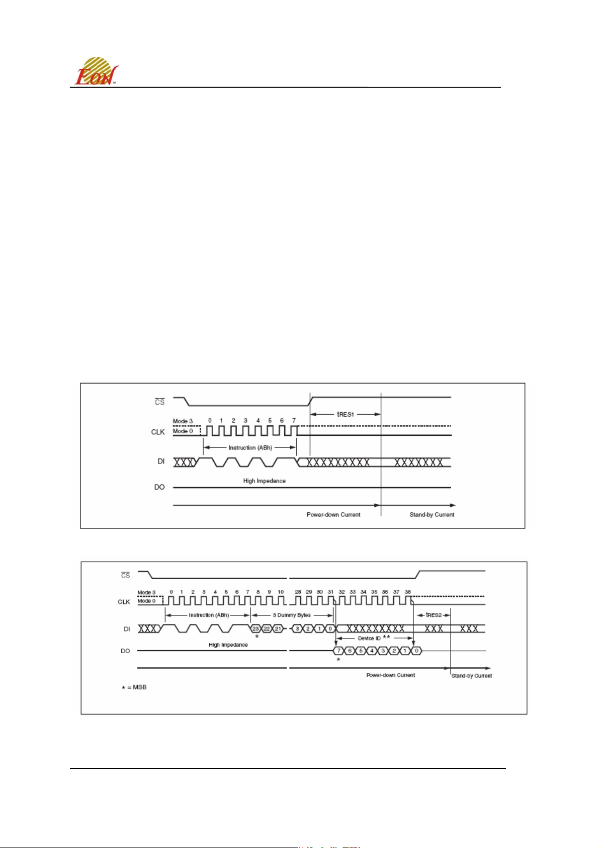
Standby mode. The Deep Power-down (DP) instruction is entered by driving Chip Select (CS#) Low,
followed by the instruction code on Serial Data Input (DI). Chip Select (CS#) must be driven Low for the
entire duration of the sequence.
The instruction sequence is shown in Figure 15..Chip Select (CS#) must be driven High after the eighth bit
of the instruction code has been latched in, otherwise the Deep Power-down (DP) instruction is not
executed. As soon as Chip Select (CS#) is driven High, it requires a delay of t
is reduced to I
CC2 and the Deep Power-down mode is entered.
before the supply current
DP
Any Deep Power-down (DP) instruction, while an Erase, Program or Write cycle is in progress, is rejected
without having any effects on the cycle that is in progress.
Figure 15. Deep Power-down Instruction Sequence Diagram
Release from Deep Power-down and Read Device ID (RDI)
Once the device has entered the Deep Power-down mode, all instructions are ignored except the Release
from Deep Power-down and Read Device ID (RDI) instruction. Executing this instruction takes the device
out of the Deep Power-down mode.
Please note that this is not the same as, or even a subset of, the JEDEC 16-bit Electronic Signature that
is read by the Read Identifier (RDID) instruction. The old-style Electronic Signature is supported for
reasons of backward compatibility, only, and should not be used for new designs. New designs should,
instead, make use of the JEDEC 16-bit Electronic Signature, and the Read Identifier (RDID) instruction.
This Data Sheet may be revised by subsequent versions ©2004 Eon Silicon Solution, Inc., www.essi.com.tw
or modifications due to changes in technical specifications.
Rev. A, Issue Date: 2006/11/6
19
Page 20
EN25T80
When used only to release the device from the power-down state, the instruction is issued by driving the
CS# pin low, shifting the instruction code “ABh” and driving CS# high as shown in Figure 16. After the
time duration of t
instructions will be accepted. The CS# pin must remain high during the t
(See AC Characteristics) the device will resume normal operation and other
RES1
time duration.
RES1
When used only to obtain the Device ID while not in the power-down state, the instruction is initiated by
driving the CS# pin low and shifting the instruction code “ABh” followed by 3-dummy bytes. The Device ID
bits are then shifted out on the falling edge of CLK with most significant bit (MSB) first as shown in Figure
17. The Device ID value for the EN25T80 are listed in Table 5. The Device ID can be read continuously.
The instruction is completed by driving CS# high.
When Chip Select (CS#) is driven High, the device is put in the Stand-by Power mode. If the device was
not previously in the Deep Power-down mode, the transition to the Stand-by Power mode is immediate. If
the device was previously in the Deep Power-down mode, though, the transition to the Standby Power
mode is delayed by t
, and Chip Select (CS#) must remain High for at least t
RES2
(max), as specified
RES2
in Table 10. Once in the Stand-by Power mode, the device waits to be selected, so that it can receive,
decode and execute instructions.
Except while an Erase, Program or Write Status Register cycle is in progress, the Release from Deep
Power-down and Read Device ID (RDI) instruction always provides access to the 8bit Device ID of the
device, and can be applied even if the Deep Power-down mode has not been entered.
Any Release from Deep Power-down and Read Device ID (RDI) instruction while an Erase, Program or
Write Status Register cycle is in progress, is not decoded, and has no effect on the cycle that is in
progress.
Figure 16. Release Power-down Instruction Sequence Diagram
Figure 17. Release Power-down / Device ID Instruction Sequence Diagram
This Data Sheet may be revised by subsequent versions ©2004 Eon Silicon Solution, Inc., www.essi.com.tw
or modifications due to changes in technical specifications.
Rev. A, Issue Date: 2006/11/6
20
Page 21
EN25T80
Read Manufacturer / Device ID (90h)
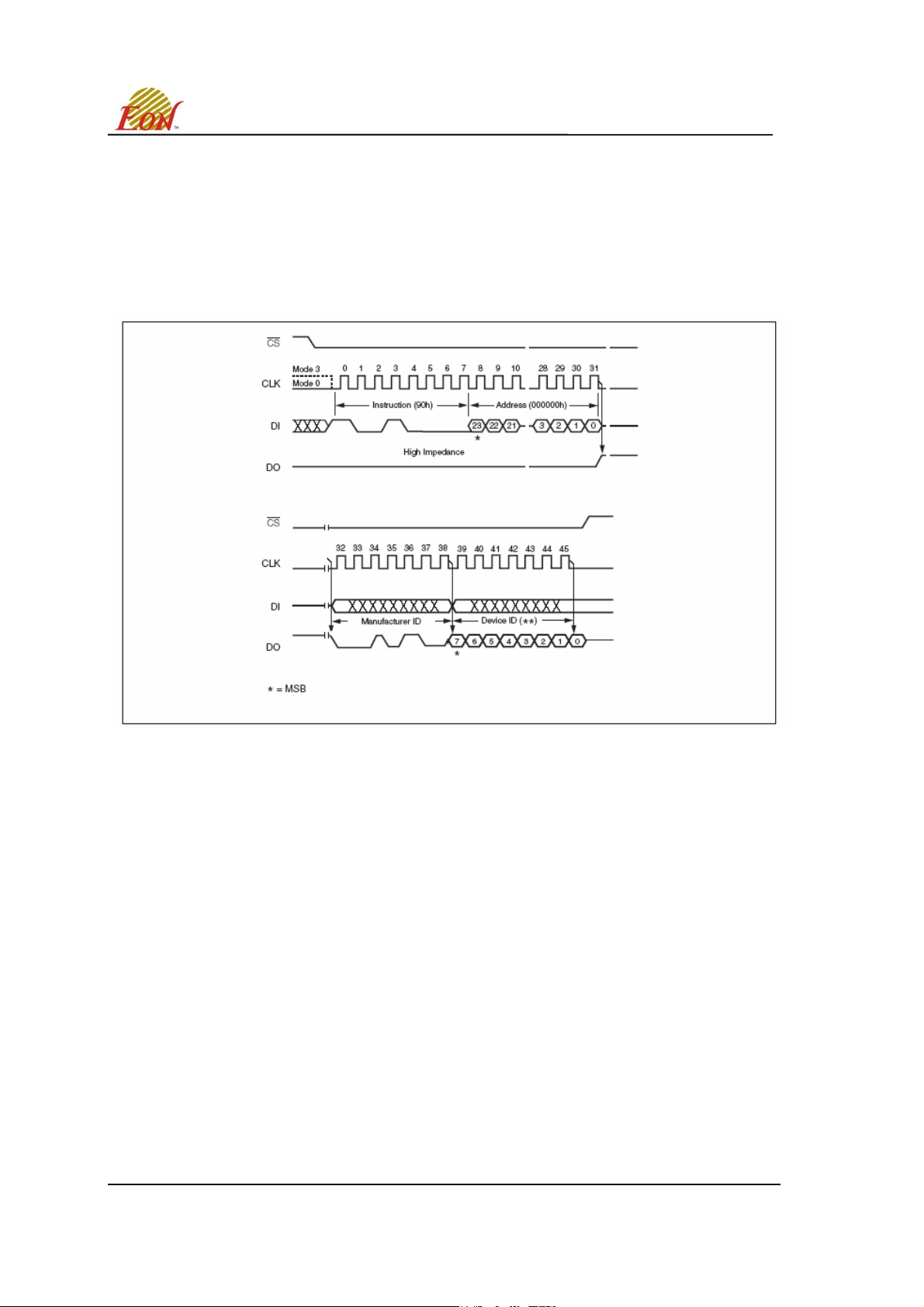
The Read Manufacturer/Device ID instruction is an alternative to the Release from Power-down / Device
ID instruction that provides both the JEDEC assigned manufacturer ID and the specific device ID.
The Read Manufacturer/Device ID instruction is very similar to the Release from Power-down / Device ID
instruction. The instruction is initiated by driving the CS# pin low and shifting the instruction code “90h”
followed by a 24-bit address (A23-A0) of 000000h. After which, the Manufacturer ID for Eon (1Ch) and the
Device ID are shifted out on the falling edge of CLK with most significant bit (MSB) first as shown in
Figure 17. The Device ID values for the EN25T8 0 are listed in Tab le 5. If the 24-bit address is initially set
to 000001h the Device ID will be read first
Figure 18. Read Manufacturer / Device ID Diagram
Read Identification (RDID)(9Fh)
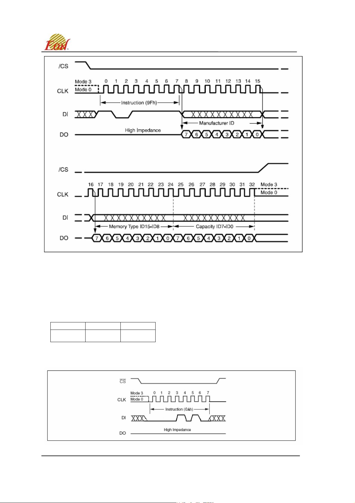
The Read Identification (RDID) instruction allows the 8-bit manufacturer identification to be read, followed
by two bytes of device identification. The device identification indicates the memory type in the first byte ,
and the memory capacity of the device in the second byte .
Any Read Identification (RDID) instruction while an Erase or Program cycle is in progress, is not decoded,
and has no effect on the cycle that is in progress. The Read Identification (RDID) instruction should not be
issued while the device is in Deep Power down mode.
The device is first selected by driving Chip Select Low. Then, the 8-bit instruction code for the instruction
is shifted in. This is followed by the 24-bit device identification, stored in the memory, being shifted out on
Serial Data Output , each bit being shifted out during the falling edge of Serial Clock . The instruction
sequence is shown in Figure 19. The Read Identification (RDID) instruction is terminated by driving Chip
Select High at any time during data output.
When Chip Select is driven High, the device is put in the Standby Power mode. Once in the Standby
Power mode, the device waits to be selected, so that it can receive, decode and execute instructions.
This Data Sheet may be revised by subsequent versions ©2004 Eon Silicon Solution, Inc., www.essi.com.tw
or modifications due to changes in technical specifications.
Rev. A, Issue Date: 2006/11/6
21
Page 22
EN25T80
Figure 19. Read Identification (RDID)
Enter EXT Mode (0Ah)
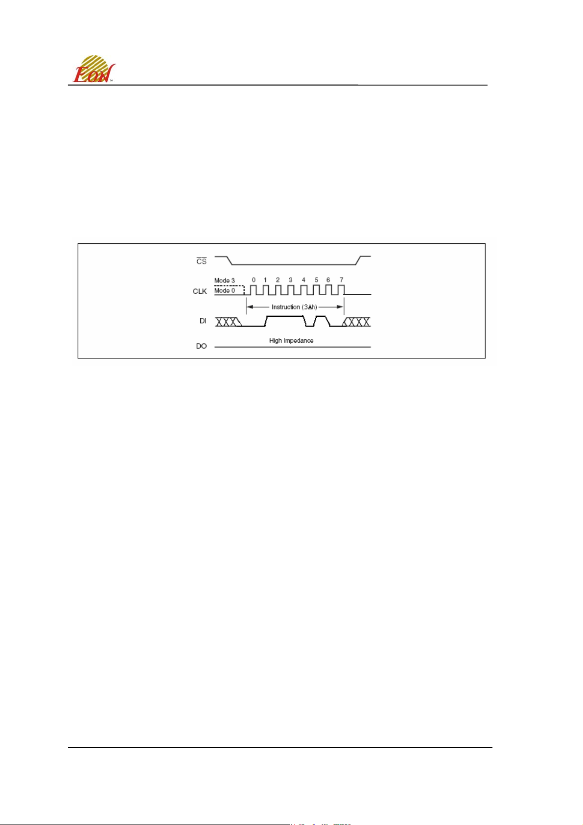
This Flash support extend transmission mode to enhance the data throughput, user can use the enter
mode commands to switch from normal mode into extend mode and exit by WRDI (04h) command. The
ENTER EXT MODE command is initiated by executing an 8-bit command 0AH. User can use RDSR
command to read the MODE bits from Status Register.
TABLE 7. Mode Table
MODE[1:0] 00 01
EXT MODE SPI
(default)
SP2
After Power On Reset, the MODE register will keep at SPI mode.
SP2 : command/address/data all transmitting with 2 bits
Figure 20. Enter EXT Mode
This Data Sheet may be revised by subsequent versions ©2004 Eon Silicon Solution, Inc., www.essi.com.tw
or modifications due to changes in technical specifications.
Rev. A, Issue Date: 2006/11/6
22
Page 23
EN25T80
Enter OTP Mode (3Ah)
This Flash has a extra 256 bytes OTP sector, user must issue ENTER OTP MODE command to enter
OTP mode before reading / programming or erasing OTP sector. After entering OTP mode, the OTP
sector is mapping to sector 255, SRP bit becomes OTP_LOCK bit and can be reading by RDSR
command. Program / Erase command will be disabled when OTP_LOCK is ‘1’
WRSR command will ignore the input data and program LOCK_BIT to 1.
User must clear the protect bits before enter OTP mode.
OTP sector can only be program and erase when LOCK_BIT equal ‘0’ and sector 255 not protected. Only
sector erase (20h) can be used to erase OTP sector. In OTP mode, user can read other sectors, but
program/erase other sectors only allowed when OTP_LOCK equal ‘0’.
User can use WRDI (04H) command to exit OTP mode.
Figure 21. Enter OTP Mode
This Data Sheet may be revised by subsequent versions ©2004 Eon Silicon Solution, Inc., www.essi.com.tw
or modifications due to changes in technical specifications.
Rev. A, Issue Date: 2006/11/6
23
Page 24
Power-up Timing
EN25T80
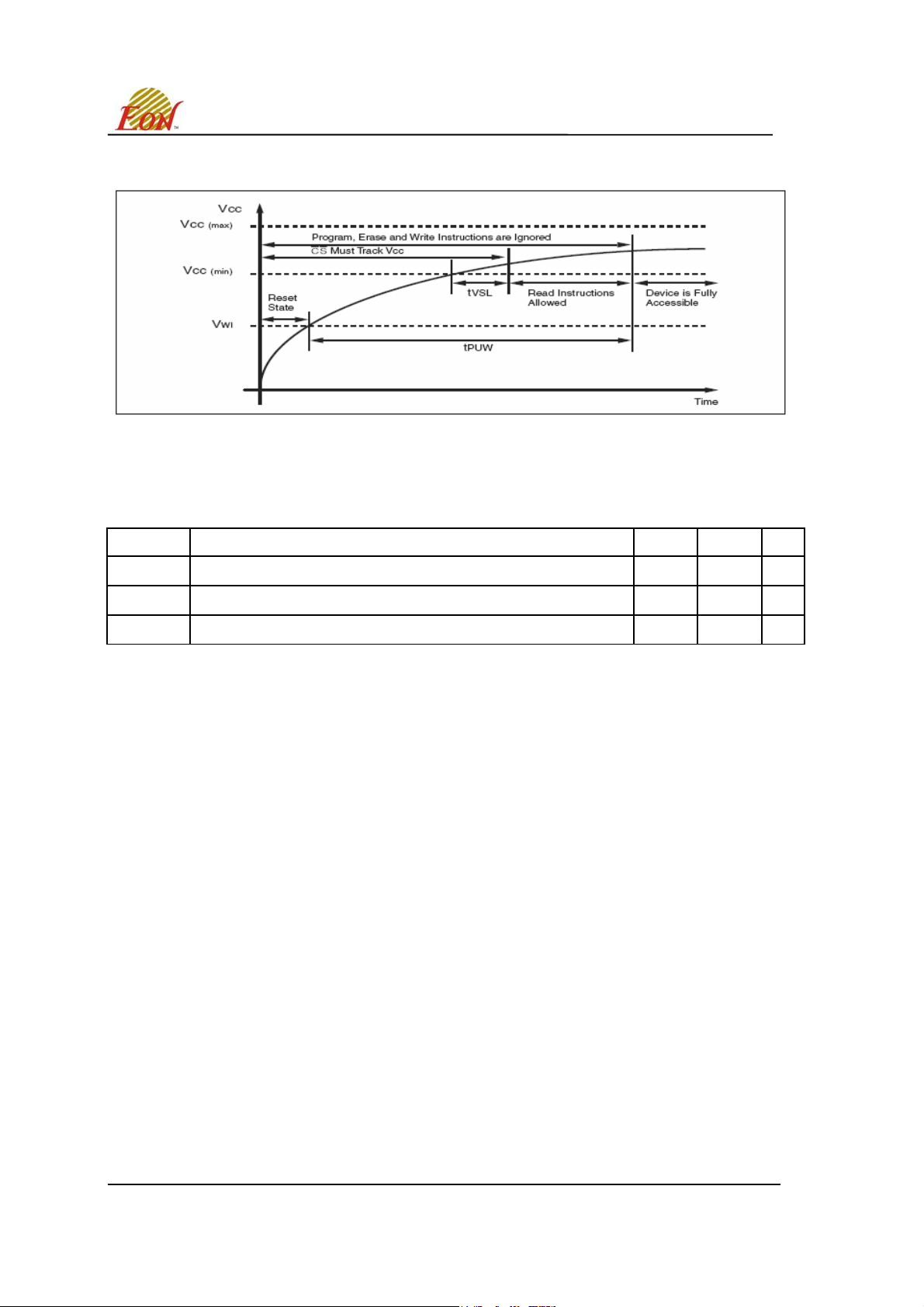
Figure 22. Power-up Timing
Table 8. Power-Up Timing and Write Inhibit Threshold
Symbol Parameter Min. Max. Unit
tVSL
tPUW
VWI
(1)
VCC(min) to CS# low 10
(1)
Time delay to Write instruction 1 10 ms
(1)
Write Inhibit Voltage 1 2 V
µs
Note:
1.The parameters are characterized only.
INITIAL DELIVERY STATE
The device is delivered with the memory array erased: all bits are set to 1 (each byte contains FF h). The
Status Register contains 00h (all Status Register bits are 0).
This Data Sheet may be revised by subsequent versions ©2004 Eon Silicon Solution, Inc., www.essi.com.tw
or modifications due to changes in technical specifications.
Rev. A, Issue Date: 2006/11/6
24
Page 25
EN25T80
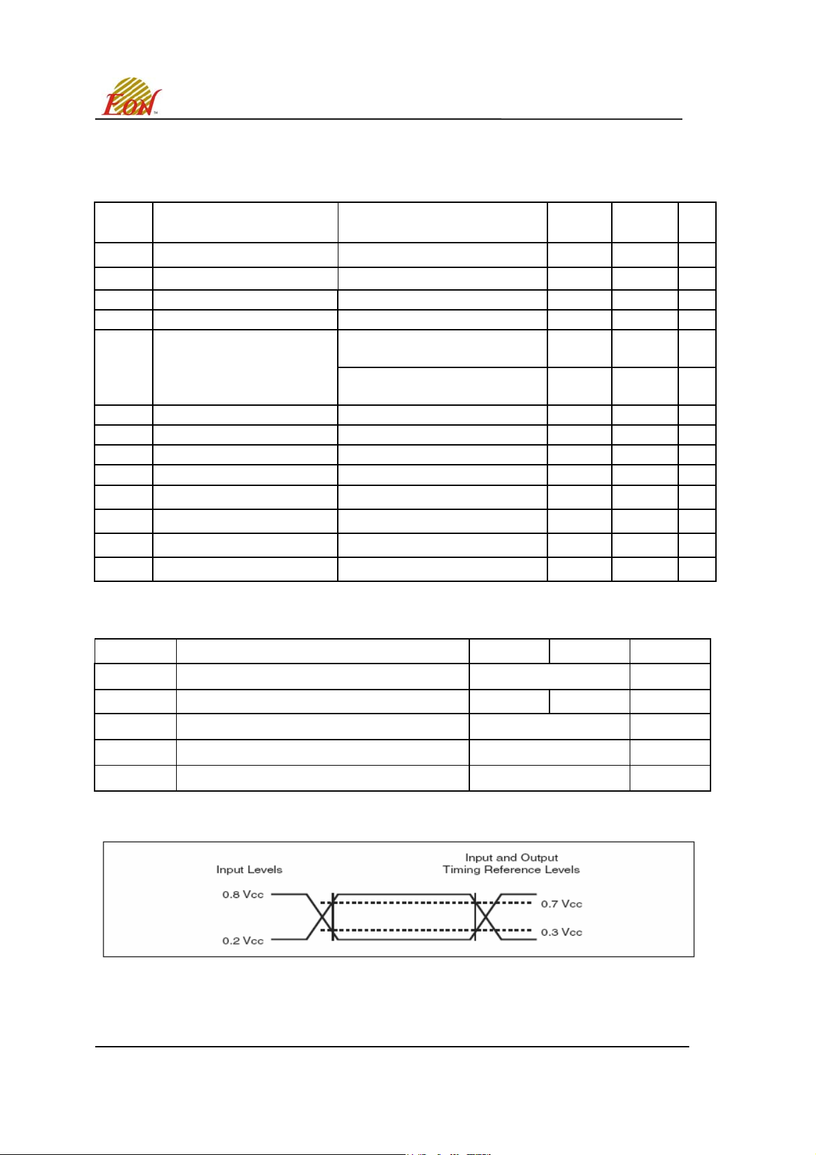
Table 9. DC Characteristics
(Ta = 0°C to 70°C or - 40°C to 85°C; VCC = 2.7-3.6V)
Symbol Parameter Test Conditions Min. Max. Unit
ILI
I
LO
I
CC1
I
CC2
I
CC3
I
CC4
I
CC5
I
CC6
I
CC7
VIL
VIH
V
OL
VOH
Input Leakage Current
Output Leakage Current
Standby Current CS# = VCC, V
Deep Power-down Current CS# = VCC, V
Operating Current (READ)
Operating Current (PP) CS# = VCC
Operating Current (WRSR) CS# = V
Operating Current (SE) CS# = V
Operating Current (BE) CS# = VCC
Input Low Voltage
Input High Voltage
Output Low Voltage
Output High Voltage
or V
= V
IN
= V
IN
CLK = 0.1 VCC / 0.9 V
SS
SS
CC
or V
at
CC
CC
100MHz, Q = open
CLK = 0.1 V
CC
/ 0.9 V
CC
at
75MHz, Q = open
± 2 µA
± 2 µA
5 µA
5 µA
25 mA
20 mA
15 mA
CC
CC
15 mA
15 mA
15 mA
IOL = 1.6 mA
– 0.5
0.7V
IOH = –100 µA VCC-0.2
VCC+0.4
CC
0.3 VCC
0.4 V
Table 10. AC Measurement Conditions
Symbol Parameter Min. Max. Unit
V
V
V
C
L
Load Capacitance 20/30 pF
Input Rise and Fall Times
Input Pulse Voltages
Input Timing Reference Voltages
Output Timing Reference Voltages
0.2
V
to 0.8VCC
CC
0.3
V
to 0.7VCC
CC
V
CC
5 ns
/ 2
Notes:
1. CL = 20 pF when CLK=100MHz, CL = 30 pF when CLK=75MHz,
Figure 23. AC Measurement I/O Waveform
This Data Sheet may be revised by subsequent versions ©2004 Eon Silicon Solution, Inc., www.essi.com.tw
or modifications due to changes in technical specifications.
Rev. A, Issue Date: 2006/11/6
25
V
V
V
Page 26
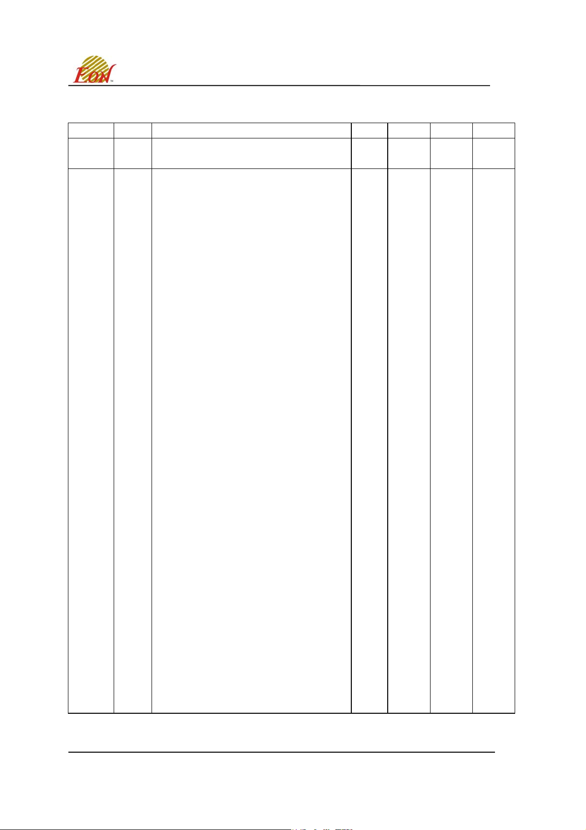
Table 11.100MHz AC Characteristics
(Ta = 0°C to 70°C or - 40°C to 85°C; VCC = 2.7-3.6V)
Symbol Alt Parameter
Serial Clock Frequency for:
FR f
FAST_READ, PP, SE, BE, DP, RES, WREN,
C
WRDI, WRSR
f
R
1
t
CLH
1
t
CLL
2
t
CLCH
2
t
CHCL
t
SLCH
t
CHSH
t
SHCH
t
CHSL
t
SHSL
2
t
SHQZ
t
CLQX
t
DVCH
t
CHDX
t
HLCH
t
HHCH
t
CHHH
t
CHHL
2
t
HLQZ
2
t
HHQZ
t
CLQV
3
t
WHSL
3
t
SHWL
2
t
DP
2
t
RES1
2
t
RES2
tW
t
PP
t
SE
tBE
t
CE
Note: 1. T
2. Value guaranteed by characterization, not 100% tested in production.
3. Only applicable as a constraint for a Write status Register instruction when Status Register Protect Bit is set at 1.
Serial Clock Frequency for READ, RDSR, RDID D.C.
Serial Clock High Time 4
Serial Clock Low Time 4
Serial Clock Rise Time (Slew Rate) 0.1
Serial Clock Fall Time (Slew Rate) 0.1
t
CS# Active Setup Time 5
CSS
CS# Active Hold Time 5
CS# Not Active Setup Time 5
CS# Not Active Hold Time 5
t
CS# High Time 100
CSH
t
Output Disable Time
DIS
tHO
t
tDH
Output Hold Time 0
Data In Setup Time 2
DSU
Data In Hold Time 5
HOLD# Low Setup Time ( relative to SCK ) 5
HOLD# High Setup Time ( relative to SCK ) 5
HOLD# Low Hold Time ( relative to SCK ) 5
HOLD# High Hold Time ( relative to SCK ) 5
tHZ
HOLD# Low to High-Z Output
tLZ
HOLD# High to Low-Z Output
tV
Output Valid from S C K
Write Protect Setup Time before CS# Low 20
Write Protect Hold Time after CS# High 100
CS# High to Deep Power-down Mode
CS# High to Standby Mode without Electronic
Signature read
CS# High to Standby Mode with Electronic
Signature read
Write Status Register Cycle Time
Page Programming Time
Sector Erase Time
Block Erase Time
Chip Erase Time
+ T
CKH
S
must be greater than or equal to 1/ F
CKL
S
CLK
Min Typ Max Unit
D.C.
ns
ns
3 µs
3 µs
1.8 µs
10 15 ms
1.5 5 ms
0.15 0.3 s
0.8 2 s
10 20 s
EN25T80
100 MHz
66 MHz
ns
ns
V / ns
V / ns
ns
ns
ns
ns
ns
6 ns
ns
ns
ns
ns
ns
ns
ns
6 ns
6 ns
6 ns
This Data Sheet may be revised by subsequent versions ©2004 Eon Silicon Solution, Inc., www.essi.com.tw
or modifications due to changes in technical specifications.
Rev. A, Issue Date: 2006/11/6
26
Page 27
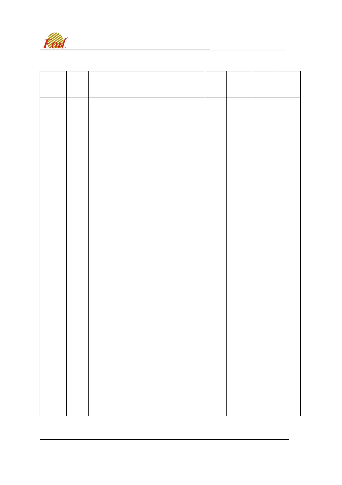
Table 12. 75MHz AC Characteristics
(Ta = 0°C to 70°C or - 40°C to 85°C; VCC = 2.7-3.6V)
Symbol Alt Parameter
Serial Clock Frequency for:
FR f
FAST_READ, PP, SE, BE, DP, RES, WREN,
C
WRDI, WRSR
f
R
1
t
CLH
1
t
CLL
2
t
CLCH
2
t
CHCL
t
SLCH
t
CHSH
t
SHCH
t
CHSL
t
SHSL
2
t
SHQZ
t
CLQX
t
DVCH
t
CHDX
t
HLCH
t
HHCH
t
CHHH
t
CHHL
2
t
HLQZ
2
t
HHQZ
t
CLQV
3
t
WHSL
3
t
SHWL
2
t
DP
2
t
RES1
2
t
RES2
tW
t
PP
t
SE
tBE
t
CE
Note: 1. T
2. Value guaranteed by characterization, not 100% tested in production.
3. Only applicable as a constraint for a Write status Register instruction when Status Register Protect Bit is set at 1.
Serial Clock Frequency for READ, RDSR, RDID D.C.
Serial Clock High Time 6
Serial Clock Low Time 6
Serial Clock Rise Time (Slew Rate) 0.1
Serial Clock Fall Time (Slew Rate) 0.1
t
CS# Active Setup Time 5
CSS
CS# Active Hold Time 5
CS# Not Active Setup Time 5
CS# Not Active Hold Time 5
t
CS# High Time 100
CSH
t
Output Disable Time
DIS
tHO
t
tDH
Output Hold Time 0
Data In Setup Time 2
DSU
Data In Hold Time 5
HOLD# Low Setup Time ( relative to SCK ) 5
HOLD# High Setup Time ( relative to SCK ) 5
HOLD# Low Hold Time ( relative to SCK ) 5
HOLD# High Hold Time ( relative to SCK ) 5
tHZ
HOLD# Low to High-Z Output
tLZ
HOLD# High to Low-Z Output
tV
Output Valid from S C K
Write Protect Setup Time before CS# Low 20
Write Protect Hold Time after CS# High 100
CS# High to Deep Power-down Mode
CS# High to Standby Mode without Electronic
Signature read
CS# High to Standby Mode with Electronic
Signature read
Write Status Register Cycle Time
Page Programming Time
Sector Erase Time
Block Erase Time
Chip Erase Time
+ T
CKH
S
must be greater than or equal to 1/ F
CKL
S
CLK
Min Typ Max Unit
D.C.
ns
ns
3 µs
3 µs
1.8 µs
10 15 ms
1.5 5 ms
0.15 0.3 s
0.8 2 s
10 20 s
EN25T80
75 MHz
66 MHz
ns
ns
V / ns
V / ns
ns
ns
ns
ns
ns
6 ns
ns
ns
ns
ns
ns
ns
ns
6 ns
6 ns
6 ns
This Data Sheet may be revised by subsequent versions ©2004 Eon Silicon Solution, Inc., www.essi.com.tw
or modifications due to changes in technical specifications.
Rev. A, Issue Date: 2006/11/6
27
Page 28
EN25T80
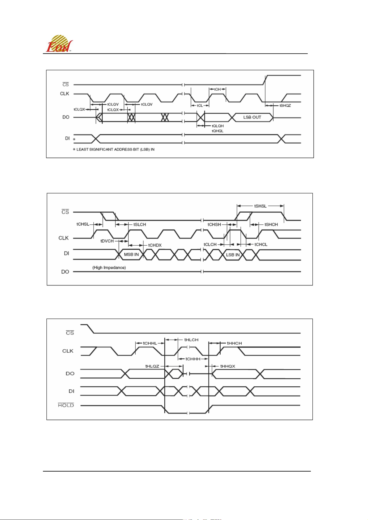
Figure 24. Serial Output Timing
Figure 25. Input Timing
Figure 26. Hold Timing
This Data Sheet may be revised by subsequent versions ©2004 Eon Silicon Solution, Inc., www.essi.com.tw
or modifications due to changes in technical specifications.
Rev. A, Issue Date: 2006/11/6
28
Page 29
EN25T80
ABSOLUTE MAXIMUM RATINGS
Stresses above the values so mentioned above may cause permanent damage to the device. These
values are for a stress rating only and do not imply that the device should be operated at conditions up to
or above these values. Exposure of the device to the maximum rating values for extended periods of time
may adversely affect the device reliability.
Parameter Value Unit
Storage Temperature -65 to +125
°C
Plastic Packages -65 to +125
Output Short Circuit Current1 200 mA
Input and Output Voltage (with respect to
ground)
2
Vcc -0.5 to +4.0 V
Notes:
1. No more than one output shorted at a time. Duration of the short circuit should not be greater than one second.
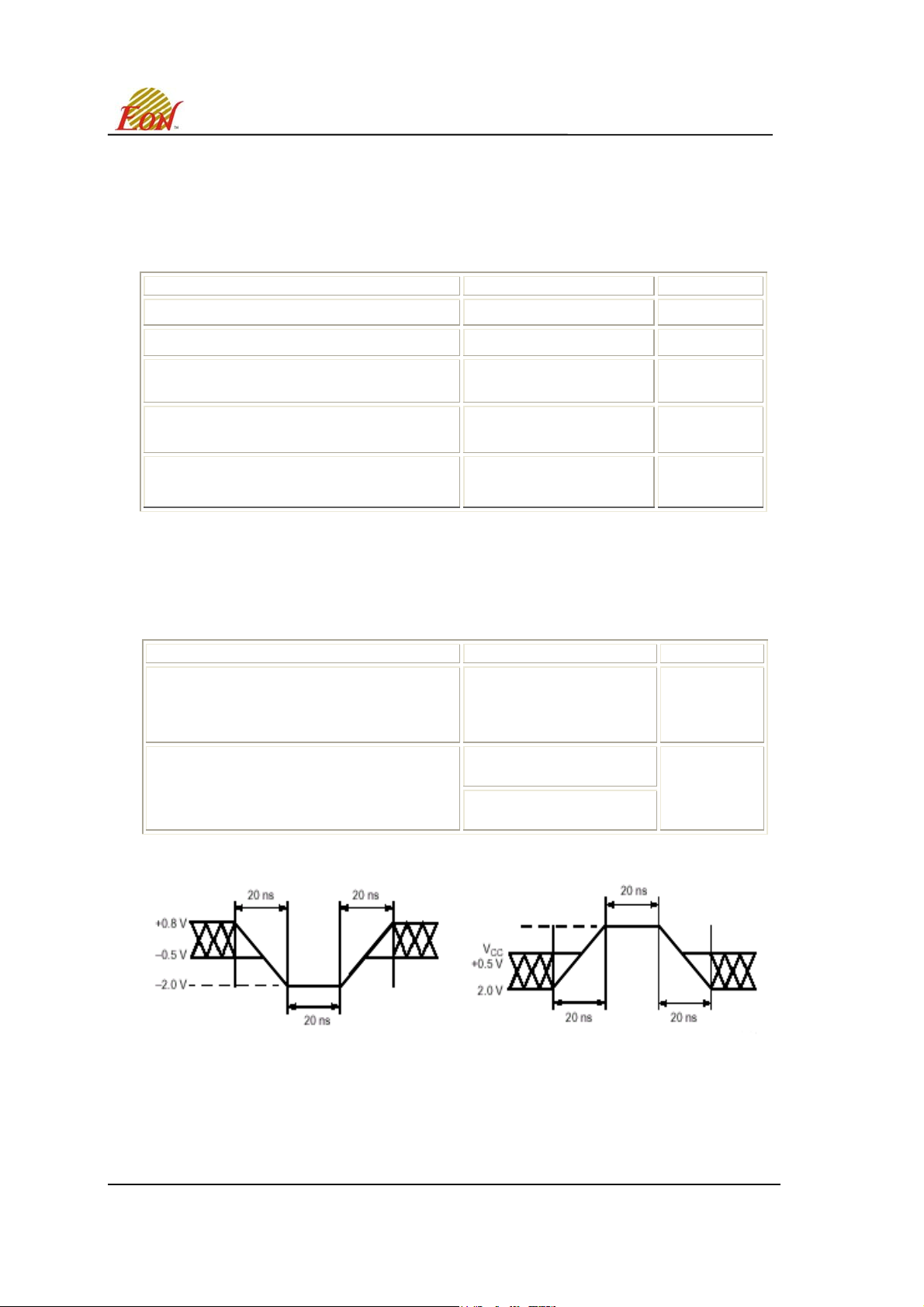
2. Minimum DC voltage o n input or I/O pins is –0.5 V. During voltage transitions, inputs may undershoot V
periods of up to 50ns and to –2.0 V for periods of up to 20ns. See figure below. Maximum DC voltage on output and I/O
pins is V
below.
+ 0.5 V. During voltage transitions, outputs may overshoot to Vcc + 1.5 V for periods up to 20ns. See figure
cc
RECOMMENDED OPERATING RANGES
Parameter Value Unit
Ambient Operating Temperature
Commercial Devices
Industrial Devices
Operating Supply Voltage
Vcc
-0.5 to +4.0 V
1
0 to 70
-40 to 85
Regulated: 3.0 to 3.6
Full: 2.7 to 3.6
°C
to –1.0V for
ss
°C
V
Notes:
1. Recommended Operating Ranges define those limits between which the functionality of the device is guaranteed.
Vcc
+1.5V
Maximum Negative Overshoot Waveform Maximum Positive Overshoot Waveform
This Data Sheet may be revised by subsequent versions ©2004 Eon Silicon Solution, Inc., www.essi.com.tw
or modifications due to changes in technical specifications.
Rev. A, Issue Date: 2006/11/6
29
Page 30
EN25T80
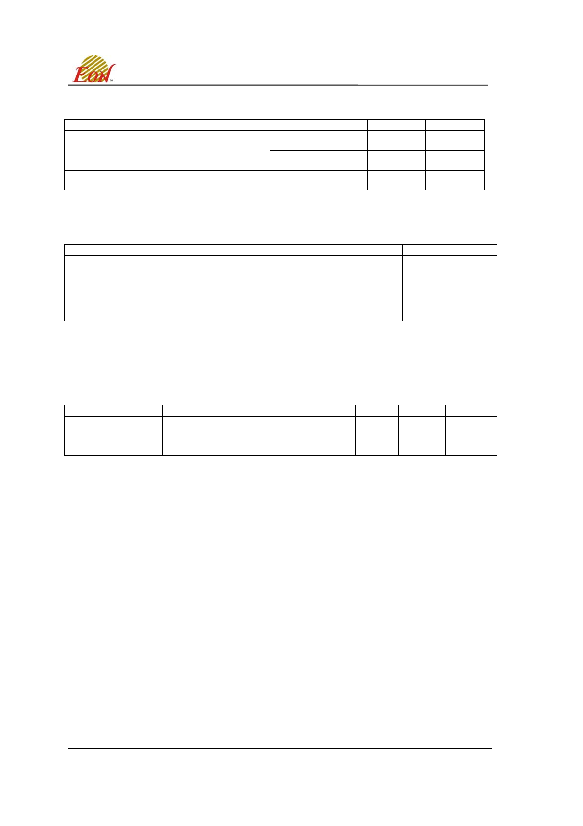
Table 13. DATA RETENTION and ENDURANCE
Parameter Description Test Conditions Min Unit
150°C 10 Years
Minimum Pattern Data Retention Time
Erase/Program Endurance -40 to 85 °C 100k cycles
125°C 20 Years
Table 14. LATCH UP CHARACTERISTICS
Parameter Description Min Max
Input voltage with respect to Vss on all pins except I/O pins
(including A9, Reset and OE#)
Input voltage with respect to Vss on all I/O Pins -1.0 V Vcc + 1.0 V
Vcc Current -100 mA 100 mA
Note : These are latch up characteristics and the device should never be put under these conditions. Refer to
Absolute Maximum ratings for the actual operating limits.
-1.0 V 12.0 V
Table 15. CAPACITANCE
( VCC = 2.7-3.6V)
Parameter Symbol Parameter Description Test Setup Typ Max Unit
CIN
Input Capacitance
VIN = 0
6 pF
C
OUT
Note : Sampled only, not 100% tested, at T
Output Capacitance
V
= 0
OUT
= 25°C and a frequency of 20MHz.
A
8 pF
This Data Sheet may be revised by subsequent versions ©2004 Eon Silicon Solution, Inc., www.essi.com.tw
or modifications due to changes in technical specifications.
Rev. A, Issue Date: 2006/11/6
30
Page 31
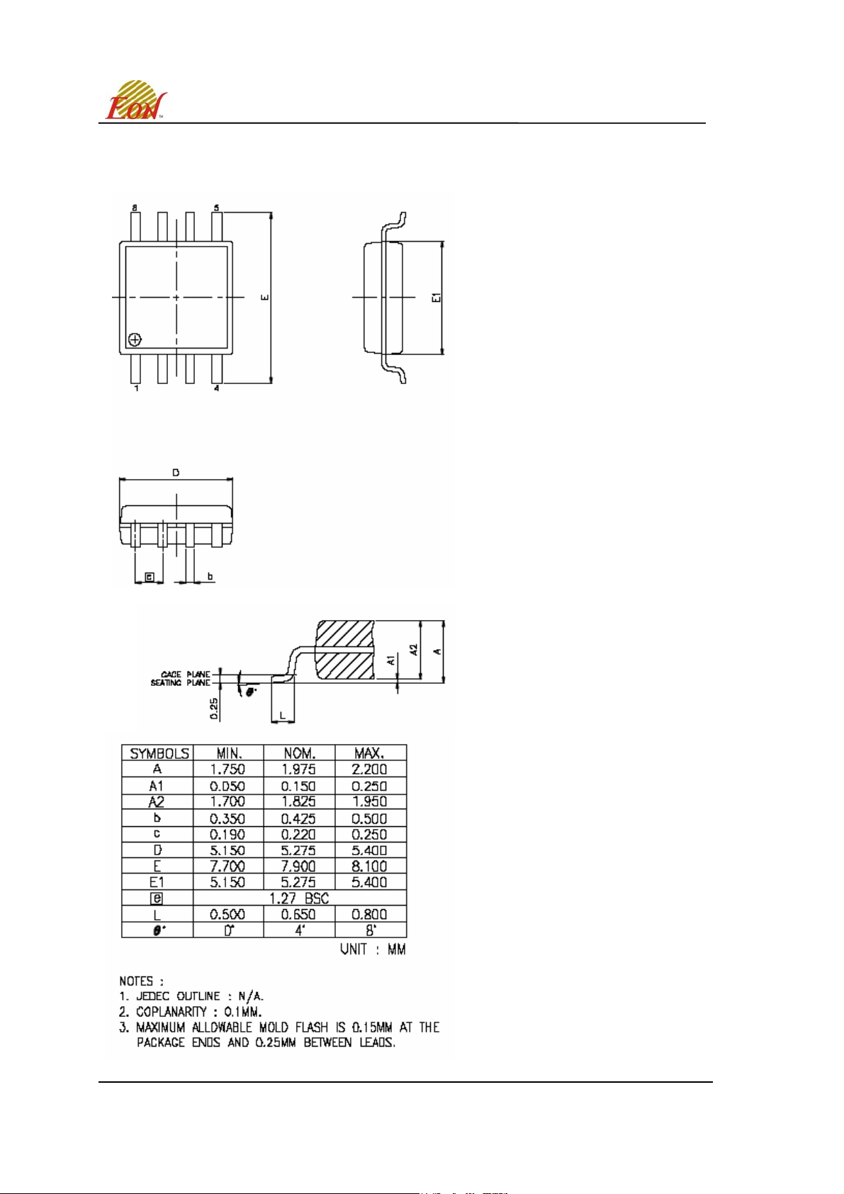
PACKAGE MECHANICAL
Figure 27. SOP 200 mil ( official name = 209 mil )
EN25T80
This Data Sheet may be revised by subsequent versions ©2004 Eon Silicon Solution, Inc., www.essi.com.tw
or modifications due to changes in technical specifications.
Rev. A, Issue Date: 2006/11/6
31
Page 32
p
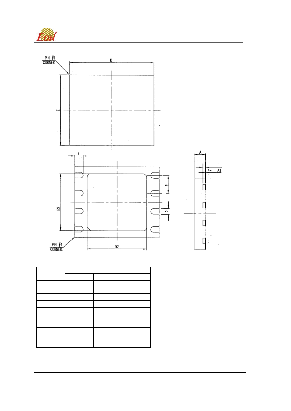
Figure 28. VDFN8( 5x6mm )
SYMBOL
A 0.76 0.80 0.84
A1 0.00 0.02 0.04
A2 - - - 0.20 - - -
D 5.90 6.00 6.10
E 4.90 5.00 5.10
D2 4.18 4.23 4.28
E2 3.95 4.00 4.05
e - - - 1.27 - - -
b 0.35 0.40 0.45
L 0.55 0.60 0.65
Note : 1. Co
lanarity: 0.1 mm
DIMENSION IN MM
MIN. NOR MAX
EN25T80
This Data Sheet may be revised by subsequent versions ©2004 Eon Silicon Solution, Inc., www.essi.com.tw
or modifications due to changes in technical specifications.
Rev. A, Issue Date: 2006/11/6
32
Page 33

EN25T80
ORDERING INFORMATION
EN25T80 - 75 H C P
PACKAGING CONTENT
(Blank) = Conventional
P = Lead-free package can represent and
warrant meeting the requirements of the
current RoHS Directive 2002/95/EC.
TEMPERATURE RANGE
C = Commercial (0°C to +70°C)
I = Industrial (-40°C to +85°C)
PACKAGE
H = 8-pin 200mil SOP
V = 8-pin VDFN
Q = 8-pin PDIP
SPEED
100 = 100 Mhz
75 = 75 Mhz
BASE PART NUMBER
EN = Eon Silicon Solution Inc.
25T = 3V Serial Small Uniform-Sector FLASH
With dual data mode
80 = 8 Megabit (1024K x 8)
This Data Sheet may be revised by subsequent versions ©2004 Eon Silicon Solution, Inc., www.essi.com.tw
or modifications due to changes in technical specifications.
Rev. A, Issue Date: 2006/11/6
33
Page 34

EN25T80
Revisions List
Revision No
A Initial release 2006/11/6
Description Date
This Data Sheet may be revised by subsequent versions ©2004 Eon Silicon Solution, Inc., www.essi.com.tw
or modifications due to changes in technical specifications.
Rev. A, Issue Date: 2006/11/6
34
 Loading...