

Page 1
EMIF09-02726Sx
Application Specific Discretes
A.S.D.
MAINAPPLICATIONS
Where EMI filtering in ESD sensitive equipmentis
required:
Computersandprinters
Communicationsystems
Mobilephones
MCU Boards
DESCRIPTION
The EMIF09-02726sxis a highly integrated array
designed to suppress EMI / RFI noise in all
systems subjected to electromagnetic
interferences.
Additionally,this filter includes an ESD protection
circuitrywhich prevents the protected device from
destruction when subjected to ESD surges up to
15kV.
BENEFITS
Cost-effectivenesscomparedto discrete
solution
EMI bi-directionallow-passfilter
Highefficiencyin ESD suppression.
Highreliabilityoffered by monolithicintegration
TM
EMI FILTER
INCLUDING ESDPROTECTION
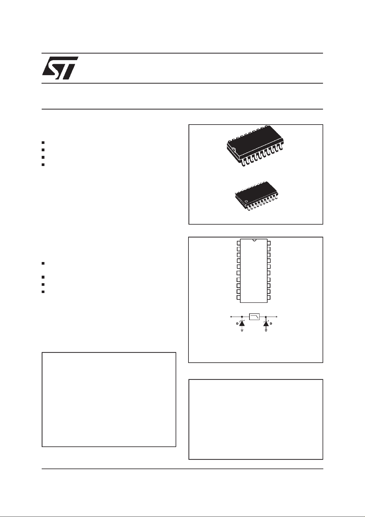
SO-20
SSOP20
PIN-OUTCONFIGURATION
I1
I2
I3
I4
I5
GND GND
I6
I7
I8
I9
9
C
E
L
L
S
O1
O2
O3
O4
O5
O6
O7
O8
O9
COMPLIESWITHTHEFOLLOWINGSTANDARD:
IEC1000-4-2
15kV (airdischarge)
8 kV (contactdischarge)
EMIF09-02726Sxfilteringresponsecurves
ASD is a trademark of STMicroelectronics
August 1999 - Ed: 2
I
DD
R
=27Ω, tolerance +/-20%
I/O
C
=130pF
IN
O
Typicalresponseto IEC1000-4-2
(16kV air discharge)
1/12
Page 2
EMIF09-02726Sx
ABSOLUTEMAXIMUM RATINGS
(T
amb
= 25°C)
Symbol Parameter Value Unit
V
PP
Maximumelectrostaticdischargein following
measurementconditions:
MILSTD 883C - METHOD3015-6
IEC1000-4-2- air discharge
IEC1000-4-2- contact discharge
P
PP
T
stg
T
j
T
OP
Peak pulse power (8/20µs) 200 W
Storagetemperaturerange
Junctiontemperature
Operatingtemperaturerange - 40 to+ 85 °C
Symbol Parameter
V
RM
V
BR
V
CL
V
F
C
IN
Stand-offvoltage
Breakdownvoltage
Clampingvoltage
Forwardvoltagedrop
Inputcapacitanceper line
Rd Dynamicimpedance
I
I
RM
PP
Leakagecurrent
Peakpulse current
V
CL
V
BR
V
RM
Slope = 1 / Rd
25
16
9
- 55to +150
150
I
I
F
V
F
I
RM
I
PP
V
kV
°C
°
C
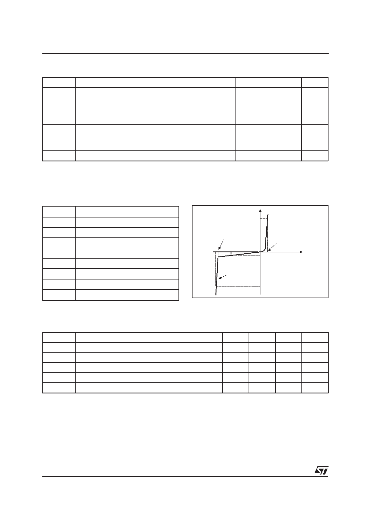
Symbol Testconditions Min. Typ. Max. Unit
I
RM
V
BR
V
F
Rd I
C 0Vbias V
Note 1: VCLcorresponds to the voltage level seen at the output pin
Note 2: Rd is given per diode
Note 3: C is given per diode
2/12
VRM= 5.25V, betweenany I/Opin and GND 20
IR=1 mA, betweenany I/O pin and GND 6.1 7.2 V
IF = 200 mA, betweenanyI/Opin and GND 1.25 V
=15A,tp= 2.5µs (note2) 0.3 Ω
PP
= 30mV F= 1MHz (note3) 130 pF
RMS
µ
A
Page 3
EMIF09-02726Sx
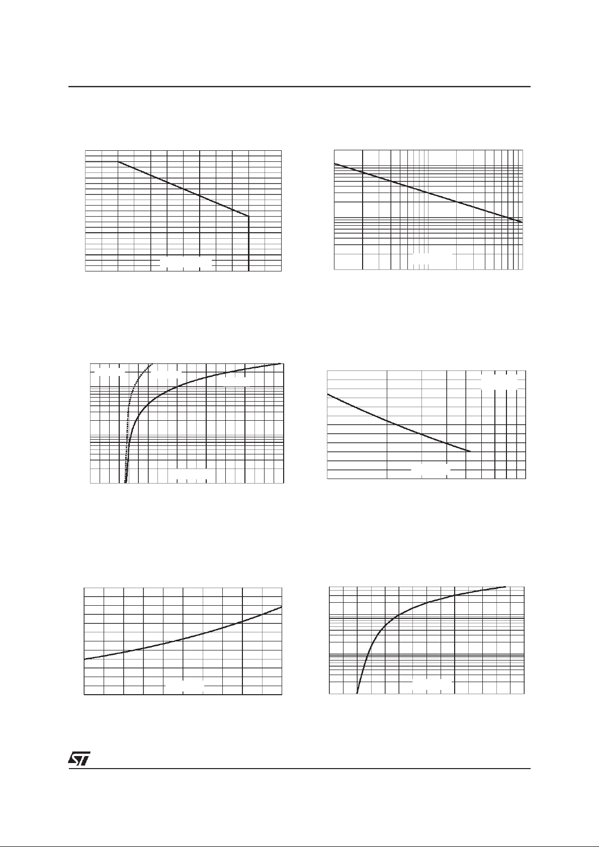
Fig. 1:
Peak power dissipation versus initial junc-
tiontemperature.
Ppp[Tj initial]/Ppp[Tj initial=25°C]
1.1
1.0
0.9
0.8
0.7
0.6
0.5
0.4
0.3
0.2
0.1
0.0
0 25 50 75 100 125 150
Fig. 3:
Clamping voltage versus peak pulse cur-
Tj initial(°C)
rent (Tjinitial=25°C).
Rectangularwaveform: tp= 2.5µs
Ipp(A)
30.0
tp=2.5µs
10.0
Output Vcl
Input Vcl
Fig.2:
Peakpulse powerversusexponentialpulse
duration(Tj initial=25°C).
Ppp(W)
2000
1000
100
tp(µs)
10
1 10 100
Fig. 4:
Input capacitance versus reverse applied
voltage(typicalvalues).
C(pF)
220
200
F=1MHz
Vosc=30mV
1.0
Vcl(V)
0.1
5 6 7 8 9 101112131415
Fig. 5:
Relativevariationof leakagecurrentversus
junctiontemperature(typicalvalues).
IR[Tj] / IR[Tj=25°C]
3.0
2.5
2.0
1.5
1.0
0.5
0.0
25 50 75 100 125 150
Tj(°C)
180
160
140
120
100
12 510
Fig.6:
Peakforwardvoltage drop versuspeak for-
VR(V)
wardcurrent(typicalvalues).
Rectangularwaveform:tp = 2.5µs
IFM(A)
5.00
1.00
0.10
VFM(V)
0.01
0.6 0.8 1.0 1.2 1.4 1.6 1.8 2.0
3/12
Page 4
EMIF09-02726Sx
ESDprotectionby the EMIF09-02726Sx
Electrostaticdischarge(ESD)is a major causeof failurein electronicsystems.
TransientVoltage Suppressorsare an ideal choice for ESD protection.They are capableof clamping the
incomingtransientto a lowenoughlevel such that damageto the protectedsemiconductoris prevented.
SurfacemountTVSarrays offer the best choicefor minimallead inductance.
Theyserve as parallel protectionelements, connected betweenthe signal line to ground.As thetransient
risesabove theoperatingvoltageof thedevice,the TVSarraybecomesa lowimpedancepathdivertingthe
transientcurrentto ground.
Fig.7:
Exampleof connectionfor one cell of theEMIF09-02726Sx
I1 O1
O2
O3
O4
Logic
Transceiver
I2
I3
I4
I5 O5
GND GND
I6 O6
I7 O7
EMIF09-02726Sx
I8 O8
I9 O9
1284-A
Connector
The EMIF09-02726Sx array is the ideal board level protection of ESD sensitive semiconductor
components.Itprovidesbestefficiencywhen usingseparatedinputsand outputs, in the socalled4-points
structure.
CircuitBoardLayout
Circuit board layout is a critical design step in the suppressionof ESD induced transients. The following
guidelinesare recommended:
The EMIF09-02726Sxshouldbe placedas near as possible tothe input terminalsor connectors.
The pathlength between theESD suppressorandthe protectedline shouldbe minimized.
Allconductive loops,including powerand groundloops shouldbe minimized.
The ESDtransientreturn path to groundshouldbe keptas short as possible.
Groundplanes should be used wheneverpossible.
Fig.8:
Transceiver,
4/12
RecommendedPCB layout to benefitfrom 4-pointstructure
TO DO
I1
O1
I2
O2
I3
O3
I4
O4
I5
O5
GND
GND
I6
O6
I7
Logic
ASIC,...
EMIF09-02726Sx
O7
I8
O8
I9
O9
footprint
Logic
Transceiver,
ASIC,...
NOT TO DO
I1
O1
I2
O2
I3
O3
I4
O4
I5
O5
GND
GND
I6
O6
I7
O7
I8
O8
I9
O9
EMIF09-02726Sx
footprint
Page 5

EMIF09-02726Sx
TECHNICAL INFORMATION
ESDPROTECTION
TheEMIF09-02726Sxis particularlyoptimizedto perform highlevel ESDprotection.The clampingvoltage
is givenby theformula:
V
CL=Vbr+Rd.IPP
Theprotectionfunctionis splittedin 2 stages.As shown in figureA1, theESD strikeis clampedby thefirst
stageS1 and then its remainingovervoltageis appliedto the secondstage throughthe resistorR. Such a
configurationmakes the output voltagevery low at theVoutlevel.
Fig.A1: ESDclamping behavior
ESD
Surge
Vg
Rg
Rd
Vin
Vbr
S1
EMIF09-02726Sx
R
Rd
Vout
Rload
Vbr
S2
Deviceto be protected
To determinethe remaining voltagesat bothVin and Voutstages, we give the typicaldynamic resistance
value Rd. Considering that : R>>Rd, Rg>>Rd and Rload>>Rd, the voltages are given by the following
formulas:
Vin
Vout
R
.
V
+
R
.
g
=
br
R.V
br
=
V
d
g
R
g
+
R
.
Vin
d
R
The result of the calculationmade for VG= 8kV, Rg= 330 Ω (IEC1000-4-2standard), Vbr=6.6V, Rd=0.3 Ω
andR=27Ωis:
Vin = 13.87V
Vout= 6.75 V
Thisconfirms the very low remaining voltageacross the deviceto be protected.It is also importantto note
that in this approximation the parasitic inductance effect was not taken into account. This could be few
tenthsof voltsduringfew nsat the Vin side.Thisparasiticeffectisnot presentat theVoutside becausethe
currentinvolvedafter the resistanceR is low.
5/12
Page 6

LATCH-UP PHENOMENA
EMIF09-02726Sx
The early aging and destruction of IC’s is often
due to latch-up phenomena which is principally
induced by dV/dt. Thanks to its RC structure, the
EMIF09-02726Sx provides a high immunity to
latch-up by integration of fast edges. (See the
response of EMIF09-02726Sx to a 1ns edge on
Fig. A3)
Themeasurementsperformedasdescribedbelow
show very clearly the high efficiency of the ESD
protection:
-no influenceof theparasiticinductancesonVout
stage
- Voutclampingvoltagevery closeto Vbr
Fig.A3:
Remainingvoltage at bothstages S1(Vin) and S2 (Vout) during ESD surge
a) Positivesurge b) Negativesurge
Fig. A2:
ESD
SURGE
Measurementconditions
EMIF09-02726Sx
R
Vin Vout
GND
GND
Itshouldbe noted that the EMIF09-02726Sxis notonly activefor positiveESD surges butalso fornegative
ones.For thiskind of disturbance,it clampsclose to groundvoltage as shown in Fig.A3b.
NOTE: DYNAMICRESISTANCEMEASUREMENT
Generallythe PCB designersneed to calculate easily the clampingvoltageVCL. This is why we give the
dynamicresistanceinaddition to theclassicalparameters.FigureA4illustratesthecurrentwaveformused
tomeasurethe Rd.
Fig.A4:
Rd measurementcurrent wave
Asthe valueofthe dynamicresistanceremains
stablefora surgedurationlower than20µs,the
I
2.5µs rectangular surge is well adapted. In
additionboth riseand falltimesareoptimizedto
avoid any parasitic phenomenon during the
PP
I
measurementof Rd.
2 µs
2.5µs
2.5µs durationmeasurement wave
6/12
tt
Page 7

EMIF09-02726Sx
FREQUENCY BEHAVIOR
In addition to the ESD protection, the EMIF09-02726Sxoffers an EMI / RFI filtering function thanksto its
Pi-filterstructure. This low-passfilter is characterizedby the followingparameters:
- Cut-offfrequency 20MHz
- Insertionloss -3dBm
- Highfrequencyrejection >-18dBm
Fig.A5:
EMIF09-02726Sxfilteringresponsecurves
Figure A5 gives these parameters, in particular the signal rejection at the 900MHz GSM frequency is
measuredatabout-21dBm(SO-20)and -26dBm(SSOP20),whilethe attenuationfor FM broadcastrange
(around100MHz)is betterthan -17dBm forboth SO-20and SSOP20.
Fig. A6: Measurementconditions
TG OUTPUT RF INPUT
TEST BOARD
120
EMIF0902726Sx
TRACKING
GENERATOR
Vg
50Ω
EMIF09
-02726Sx
SPECTRUM
ANALYSER
VoutVin
50Ω
7/12
Page 8

CROSSTALK BEHAVIOR
1- Crosstalkphenomena
Fig.A7: Crosstalkphenomena
R
G1
EMIF09-02726Sx
line 1
V
G1
R
G2
V
G2
line 2
R
L2
R
L1
α
V
2
α β
+
G2
V
1
G1
β
21
V
+
G2
12
V
G1
DRIVERS RECEIVERS
The crosstalk phenomena are due to the coupling between 2 lines. The coupling factor ( β12 or β21 )
increases when the gap across lines decreases, particularly in silicon dice. In the example above the
expectedsignal onload RL2isα2VG2,in fact the real voltageat thispointhas gotan extravalueβ21VG1.
This part of the VG1 signal representsthe effect of the crosstalk phenomenonof the line 1 on the line 2.
Thisphenomenonhasto be takeninto accountwhenthe driversimposefastdigitaldata or highfrequency
analog signals in the disturbingline. The perturbed line will be more affected if it works with low voltage
signalor high load impedance (few kΩ). The following chapters give the value of both digital and analog
crosstalk.
2- Digital Crosstalk
Fig.A8: Digitalcrosstalk measurements
+5V +5V
EMIF09-02726Sx
74HC04 74HC04
Line 1
V
Square
+5V
G1
Pulse
Generator
5KHz
Line 2
β
V
G1
21
Figure A8 shows the measurement circuit used to quantify the crosstalk effect in a classical digital
application.
Figure A9 shows that in thecase of a signalfrom 0 to 5V with a rise timeof a fewtenths of ns, the impact
onthe disturbed line is lessthan100mV peakto peak. No data disturbanceis noted on theconcernedline.
Thesame results areobtained with fallingedges.
Note:
Themeasurementshave been performedin the worst casei.e. on twoadjacent cells(1/20 & 2/19).
8/12
Page 9

EMIF09-02726Sx
Fig. A9: Digitalcrosstalkresults
3- AnalogCrosstalk
Fig.A10: Analogcrosstalkmeasurements
TG OUTPUT
TEST BOARD
1
EMIF0902726Sx
RF INPUT
19
Fig. A11: Typicalanalog crosstalkresults
Figure A10 gives the measurement circuit for the analogapplication. In figure A11, the curves show the
effectof cell 1/20oncell 2/19,nodifferenceis foundwithothercouplesof adjacentcells. In usualfrequency
rangeofanalogsignals(up to 100MHz)theeffecton disturbedlineis lessthan -32dBmforSO-20package
and-37dBmfor SSOP20package.
9/12
Page 10

4- PSpice model
Fig.A12:
PSpicemodelofoneEMIF09-02726Sxcell
EMIF09-02726Sx
IN OUT
5nH 5nH
Dz
Dr Dr
27Ω
Df Df
Dz
Lg
GND
Figure A12 shows the PSpice model of one cell of the EMIF09-02726Sx. In this model, the diodes are
definedby thefollowingPSpice parameters:
Dz Df Dr
BV 5.6 1000 1000
Cjo 130p 130p 1p
IBV 1m 100u 100u
IKF 1000 0 1000
IS 10E-21 2.0861E-21 10E-15
ISR 1p 1n 100p
N 1 1 0.6
M 0.3333 0.3333 0.3333
RS 0.3 0.3 1m
VJ 0.6 0.6 0.6
TT 1u 1u 1n
Note: This simulation model is given foran ambient temperature of 27°C.
Thevalue of Lg is dependingon thepackage:
SSOP20 --> Lg=0.7nH
SO-20 --> Lg=1.4nH
Thecomparisonbetweenthe PSpicesimulationandthe measuredfrequencyresponseis giveninfig A13a
& A13b.Thisshows that the PSpicemodel isvery closeto the product behavior.
Fig. A13:
10/12
ComparisonbetweenPSpice simulationand measuredfrequencyresponse
a) SSOP20Package
5nH 5nH
IN OUT
Dz DzDf Df
Dr Dr
27
GND
Ω
Lg
b) SO-20Package
Page 11

EMIF09-02726Sx
PART NUMBERING AND ORDERING INFORMATION
EMIF 09 027 26 S 3-
EMI FILTERING
9 BitsWide
PACKAGEMECHANICAL DATA
SO-20 (Plastic)
D
R value ( )Ω
REF.
hx45°
Surface mount
C/10
2 x 130pF = 260pF
Package:
3: SO-20
6: SSOP20
DIMENSIONS
Millimeters Inches
Min. Typ. Max. Min. Typ. Max.
A
K
e
A1B
L
A 2.35 2.65 0.092 0.104
A1 0.10 0.20 0.004 0.008
C
B 0.33 0.51 0.013 0.020
C 0.23 0.32 0.009 0.013
D 12.6 13.0 0.484 0.512
EH
E 7.40 7.60 0.291 0.299
e 1.27 0.050
H 10.0 10.65 0.394 0.419
h 0.25 0.75 0.010 0.029
L 0.50 1.27 0.020 0.050
K8°(max)
11/12
Page 12

PACKAGEMECHANICAL DATA
SSOP20 (Plastic)
EMIF09-02726Sx
DIMENSIONS
b
D
20
ORDERINGCODE
REF.
L
Millimeters Inches
Min. Typ. Max. Min. Typ. Max.
A 2.00 0.079
A2
A
e
k
E
A1 c
A1 0.25 0.010
A2 1.51 2.00 0.059 0.079
b 0.25 0.30 0.35 0.010 0.012 0.014
c 0.10 0.35 0.004 0.014
11
E1
101
D 7.05 8.05 0.278 0.317
E 7.60 8.70 0.299 0.343
E1 5.02 6.10 6.22 0.198 0.240 0.245
e 0.65 0.026
k0° 10° 0° 10°
L 0.25 0.50 0.80 0.010 0.020 0.031
Ordercode Marking Package Weight
Delivery
mode
Base qty
(pcs)
EMIF09-02726S3 ESDR6V1-27 SO-20 0.52g. Tube 50
EMIF09-02726S6 ESDR6V1-27 SSOP20 0.18g. Tube 50
Informationfurnishedis believedto beaccurate and reliable.However, STMicroelectronics assumes no responsibility for the consequences of
use of such informationnor for any infringementof patentsor otherrights of third parties which may result from its use. No license is granted by
implication or otherwise under any patent or patent rights of STMicroelectronics. Specifications mentioned in this publication are subject to
change without notice. This publicationsupersedes and replaces all information previously supplied.
STMicroelectronics products are not authorized for use as critical components in lifesupport devices or systems without express written approval of STMicroelectronics.
The ST logois a registeredtrademark ofSTMicroelectronics
1999 STMicroelectronics - Printed in Italy - All rights reserved.
STMicroelectronics GROUP OF COMPANIES
Australia - Brazil - Canada - China - France - Germany - Italy - Japan - Korea - Malaysia - Malta - Mexico - Morocco -
The Netherlands - Singapore - Spain -Sweden - Switzerland - Taiwan - Thailand - United Kingdom - U.S.A.
http://www.st.com
12/12
 Loading...