

Page 1

6121 Baker Road,
Suite 108
Minnetonka, MN 55345
www.chtechnology.com
Phone (952) 933-6190
Fax (952) 933-6223
1-800-274-4284
Thank you for downloading this document from C&H Technology, Inc.
Please contact the C&H Technology team for the following questions -
Technical
Application
Assembly
Availability
Pricing
Phone – 1-800-274-4284
E-Mail – [email protected]
www.chtechnology.com - SPECIALISTS IN POWER ELECTRONIC COMPONENTS AND ASSEMBLIES - www.chtechnology.com
Page 2
www.vishay.com
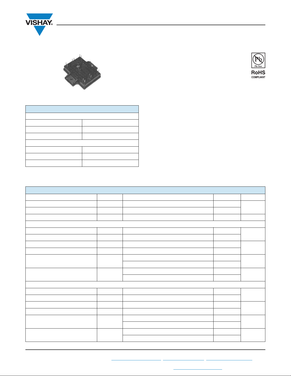
EMIPAK2
3-Levels Half-Bridge Inverter Stage, 60 A/57 A
PRODUCT SUMMARY
1° LEVEL OF HALF-BRIDGE
V
CES
typical at IC = 50 A 1.8 V
V
CE(ON)
I
at TC = 98 °C 50 A
C
2° LEVEL OF HALF-BRIDGE
V
CES
typical at IC = 50 A 2.73 V
V
CE(ON)
I
at TC = 93 °C 50 A
C
600 V
900 V
VS-EMF050J60U
Vishay Semiconductors
FEATURES
• Warp1 and Warp2 PFC IGBT
®
•FRED Pt
•FRED Pt
• Integrated thermistor
•Square RBSOA
• Operating frequency 60 kHz to 150 kHz
• Low internal inductances
• Low switching loss
• Compliant to RoHS Directive 2002/95/EC
DESCRIPTION
VS-EMF050J60U is an integrated solution for a multi level
inverter half-bridge in a single package. The EMIPAK2
package is easy to use thanks to the solderable terminals
and provides improved thermal performance thanks to the
exposed substrate. The optimized layout also helps to
minimize stray parameters, allowing for better EMI
performance.
and HEXFRED® antiparallel diodes
®
clamping diodes
ABSOLUTE MAXIMUM RATINGS
PARAMETER SYMBOL TEST CONDITIONS MAX. UNITS
Operating junction temperature T
Storage temperature range T
RMS isolation voltage V
Q1 - Q4 IGBT
Collector to emitter voltage V
Gate to emitter voltage V
Pulsed collector current I
Clamped inductive load current I
LM
Continuous collector current I
Power dissipation P
Q2 - Q3 IGBT
Collector to emitter voltage V
Gate to emitter voltage V
Pulsed collector current I
Clamped inductive load current I
LM
Continuous collector current I
Power dissipation P
J
Stg
ISOL
CES
GES
CM
(1)
TJ = 25 °C, all terminals shorted, f = 50 Hz, t = 1 s 3500 V
20
TC = 25 °C 88
C
T
= 80 °C 60
C
TC = 25 °C 338
D
CES
GES
CM
(2)
T
= 80 °C 189
C
TC = 25 °C 85
C
T
= 80 °C 57
C
TC = 25 °C 338
D
T
= 80 °C 189
C
150
- 40 to 125
600
150
150
900
20
150
150
°C
V
A
A
W
V
A
A
W
Revision: 09-Dec-11
For technical questions within your region: [email protected]
1
Document Number: 93494
THIS DOCUMENT IS SUBJECT TO CHANGE WITHOUT NOTICE. THE PRODUCTS DESCRIBED HEREIN AND THIS DOCUMENT
ARE SUBJECT TO SPECIFIC DISCLAIMERS, SET FORTH AT www.vishay.com/doc?91000
Page 3
VS-EMF050J60U
www.vishay.com
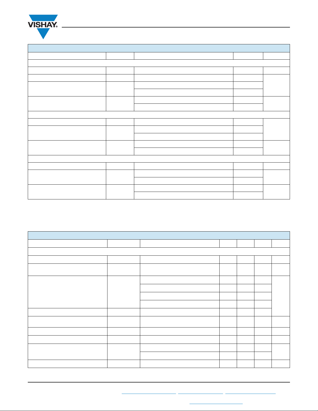
ABSOLUTE MAXIMUM RATINGS
PARAMETER SYMBOL TEST CONDITIONS MAX. UNITS
D1 - D2 CLAMPING DIODE
Repetitive peak reverse voltage V
Single pulse forward current I
Diode continuous forward current I
Power dissipation P
D3 - D4 AP DIODE
Single pulse forward current I
Diode continuous forward current I
Power dissipation P
D5 - D6 AP DIODE
Single pulse forward current I
Diode continuous forward current I
Power dissipation P
Notes
• Absolute Maximum Ratings indicate sustained limits beyond which damage to the device may occur.
(1)
V
(2)
CC
V
CC
= 400 V, V
= 720 V, V
= 15 V, L = 500 μH, Rg = 22 , TJ = 150 °C
GE
= 15 V, L = 500 μH, Rg = 22 , TJ = 150 °C
GE
RRM
FSM
F
FSM
F
FSM
F
10 ms sine or 6 ms rectangular pulse, TJ = 25 °C 270
TC = 25 °C 68
T
= 80 °C 46
C
TC = 25 °C 150
D
T
= 80 °C 84
C
10 ms sine or 6 ms rectangular pulse, TJ = 25 °C 280
TC = 25 °C 53
= 80 °C 36
T
C
TC = 25 °C 176
D
T
= 80 °C 99
C
10 ms sine or 6 ms rectangular pulse, TJ = 25 °C 220 A
TC = 25 °C 46
T
= 80 °C 31
C
TC = 25 °C 96
D
T
= 80 °C 54
C
Vishay Semiconductors
600 V
A
W
A
W
A
W
ELECTRICAL SPECIFICATIONS (TJ = 25 °C unless otherwise noted)
PARAMETER SYMBOL TEST CONDITIONS MIN. TYP. MAX. UNITS
Q1 - Q4 IGBT
Collector to emitter breakdown voltage BV
Temperature coefficient of breakdown
voltage
Collector to emitter voltage V
Gate threshold voltage V
Temperature coefficient of threshold
voltage
Forward transconductance g
Transfer characteristics V
Zero gate voltage collector current I
Gate to emitter leakage current I
BV
V
CES
CE(ON)
GE(th)
GE(th)
CES
GES
CES
/T
/T
fe
GE
Revision: 09-Dec-11
For technical questions within your region: [email protected]
THIS DOCUMENT IS SUBJECT TO CHANGE WITHOUT NOTICE. THE PRODUCTS DESCRIBED HEREIN AND THIS DOCUMENT
ARE SUBJECT TO SPECIFIC DISCLAIMERS, SET FORTH AT www.vishay.com/doc?91000
VGE = 0 V, IC = 500 μA 600 - - V
VGE = 0 V, IC = 500 μA (25 °C to 125 °C) - 0.1 - V/°C
J
VGE = 15 V, IC = 27 A - 1.44 1.75
= 15 V, IC = 50 A - 1.8 2.1
V
GE
= 15 V, IC = 27 A, TJ = 125 °C - 1.7 2.05
V
GE
= 15 V, IC = 50 A, TJ = 125 °C - 2.2 2.5
V
GE
VCE = VGE, IC = 250 μA 2.9 3.9 5.3
VCE = VGE, IC = 1 mA (25 °C to 125 °C) - - 10 - mV/°C
J
VCE = 20 V, IC = 50 A - 95 - s
VCE = 20 V, IC = 50 A - 5.9 - V
VGE = 0 V, VCE = 600 V - 0.003 0.1
V
= 0 V, VCE = 600 V, TJ = 125 °C - 0.170 3
GE
VGE = ± 20 V, VCE = 0 V - - ± 200 nA
2
Document Number: 93494
V
mA
Page 4
VS-EMF050J60U
www.vishay.com
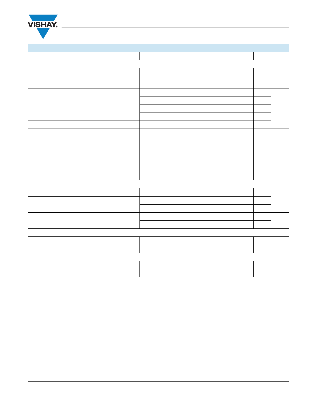
ELECTRICAL SPECIFICATIONS (TJ = 25 °C unless otherwise noted)
PARAMETER SYMBOL TEST CONDITIONS MIN. TYP. MAX. UNITS
Q2 - Q3 IGBT
Collector to emitter breakdown voltage BV
Temperature coefficient of breakdown
voltage
BV
Collector to emitter voltage V
Gate threshold voltage V
Temperature coefficient of threshold
voltage
V
GE(th)
Forward transconductance g
Transfer characteristics V
Zero gate voltage collector current I
Gate to emitter leakage current I
D1 - D2 CLAMPING DIODE
Cathode to anode blocking voltage V
Forward voltage drop V
Reverse leakage current I
D3 - D4 AP DIODE
Forward voltage drop V
D5 - D6 AP DIODE
Forward voltage drop V
CES
CES
CE(ON)
GE(th)
fe
GE
CES
GES
BR
FM
RM
FM
FM
/T
/T
VGE = 0 V, IC = 500 μA 900 - - V
VGE = 0 V, IC = 500 μA (25 °C to 125 °C) - - 8.5 - V/°C
J
VGE = 15 V, IC = 27 A - 2.45 2.8
= 15 V, IC = 50 A - 2.73 3.2
V
GE
= 15 V, IC = 27 A, TJ = 125 °C - 2 2.35
V
GE
= 15 V, IC = 50 A, TJ = 125 °C - 2.43 2.9
V
GE
VCE = VGE, IC = 250 μA 2.8 4.5 6.3
VCE = VGE, IC = 1 mA (25 °C to 125 °C) - - 11.7 - mV/°C
J
VCE = 20 V, IC = 50 A - 68 - s
VCE = 20 V, IC = 50 A - 6.9 - V
VGE = 0 V, VCE = 900 V - 0.006 0.38
V
= 0 V, VCE = 900 V, TJ = 125 °C - 1.4 3
GE
VGE = ± 20 V, V
= 0 V - - ± 200 nA
CE
IR = 100 μA 600 - -
IF = 30 A - 1.84 2.12
= 30 A, TJ = 125 °C - 1.37 1.65
I
F
VR = 600 V - 0.002 0.1
V
= 600 V, TJ = 125 °C - 0.9 6
R
IF = 50 A - 2.7 3.2
I
= 50 A TJ = 125 °C - 2.8 3.3
F
IF = 30 A - 1.93 2.37
I
= 30 A TJ = 125 °C - 1.48 1.9
F
Vishay Semiconductors
V
mA
V
mA
V
V
Revision: 09-Dec-11
For technical questions within your region: [email protected]
3
Document Number: 93494
THIS DOCUMENT IS SUBJECT TO CHANGE WITHOUT NOTICE. THE PRODUCTS DESCRIBED HEREIN AND THIS DOCUMENT
ARE SUBJECT TO SPECIFIC DISCLAIMERS, SET FORTH AT www.vishay.com/doc?91000
Page 5
VS-EMF050J60U
www.vishay.com
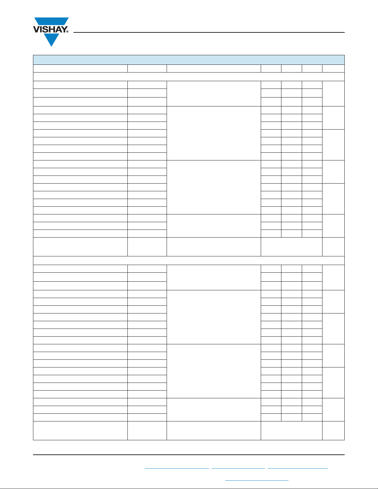
SWITCHING CHARACTERISTICS (TJ = 25 °C unless otherwise noted)
PARAMETER SYMBOL TEST CONDITIONS MIN. TYP. MAX. UNITS
Q1 - Q4 IGBT (WITH FREEWHEELING D1 - D2 CLAMPING DIODE)
Total gate charge (turn-on) Q
Gate to ermitter charge (turn-on) Q
Gate to collector charge (turn-on) Q
Turn-on switching loss E
Total switching loss E
Turn-on delay time t
Rise time t
Turn-off delay time t
Fall time t
Turn-on switching loss E
Total switching loss E
Turn-on delay time t
Rise time t
Turn-off delay time t
Fall time t
Input capacitance C
Reverse transfer capacitance C
Reverse bias safe operating area RBSOA
Q2 - Q3 IGBT (WITH FREEWHEELING D3 - D4 AP DIODE)
Total gate charge (turn-on) Q
Gate to emitter charge (turn-on) Q
Gate to collector charge (turn-on) Q
Turn-on switching loss E
Total switching loss E
Turn-on delay time t
Rise time t
Turn-off delay time t
Fall time t
Turn-on switching loss E
Total switching loss E
Turn-on delay time t
Rise time t
Turn-off delay time t
Fall time t
Input capacitance C
Reverse transfer capacitance C
Reverse bias safe operating area RBSOA
ge
gc
ON
OFF
TOT
d(on)
d(off)
ON
OFF
TOT
d(on)
d(off)
ies
oes
res
ge
gc
ON
OFF
TOT
d(on)
d(off)
ON
OFF
TOT
d(on)
d(off)
ies
oes
res
g
IC= 70 A
= 400 V
V
CC
= 15 V
V
GE
IC = 50 A
V
= 400 V
CC
V
= 15 V
GE
= 4.7
R
r
f
g
L = 500 μH
(1)
IC = 50 A
= 400 V
V
CC
V
= 15 V
GE
R
= 4.7
r
f
g
L = 500 μH
= 125 °C
T
J
(1)
VGE = 0 V
V
= 30 V
CC
f = 1 MHz
T
= 150 °C, IC = 150 A
J
V
= 400 V, VP = 600 V
CC
R
= 22 , V
g
g
IC= 50 A
= 400 V
V
CC
= 15 V
V
GE
= 15 V to 0 V
GE
IC = 50 A
= 720 V
V
CC
= 15 V
V
GE
R
= 4.7
r
f
g
L = 500 μH
(1)
IC = 50 A
= 720 V
V
CC
V
= 15 V
GE
= 4.7
R
r
f
g
L = 500 μH
T
= 125 °C
J
(1)
VGE = 0 V
= 30 V
V
CC
f = 1 MHz
T
= 150 °C, IC = 150 A
J
V
= 720 V, VP = 900 V
CC
R
= 22 , V
g
= 15 V to 0 V
GE
Vishay Semiconductors
- 480 720
- 82 164
- 160 260
-0.11-
-0.76-
-0.87-
- 182 -
-46-
- 207 -
-92-
-0.25-
-0.88-
-1.13-
- 183 -
-47-
- 211 -
- 101 -
- 9500
- 780
- 116
Fullsquare
- 320 480
-3858
- 106 160
-0.56-
-0.68-
-1.24-
- 152 -
-48-
- 165 -
- 100 -
-0.95-
-2.18-
-3.13-
- 154 -
-52-
- 168 -
- 360 -
- 6600 -
- 400 -
-90-
Fullsquare
nC
mJTurn-off switching loss E
ns
mJTurn-off switching loss E
ns
pFOutput capacitance C
nC
mJTurn-off switching loss E
ns
mJTurn-off switching loss E
ns
pFOutput capacitance C
Revision: 09-Dec-11
For technical questions within your region: [email protected]
4
Document Number: 93494
THIS DOCUMENT IS SUBJECT TO CHANGE WITHOUT NOTICE. THE PRODUCTS DESCRIBED HEREIN AND THIS DOCUMENT
ARE SUBJECT TO SPECIFIC DISCLAIMERS, SET FORTH AT www.vishay.com/doc?91000
Page 6
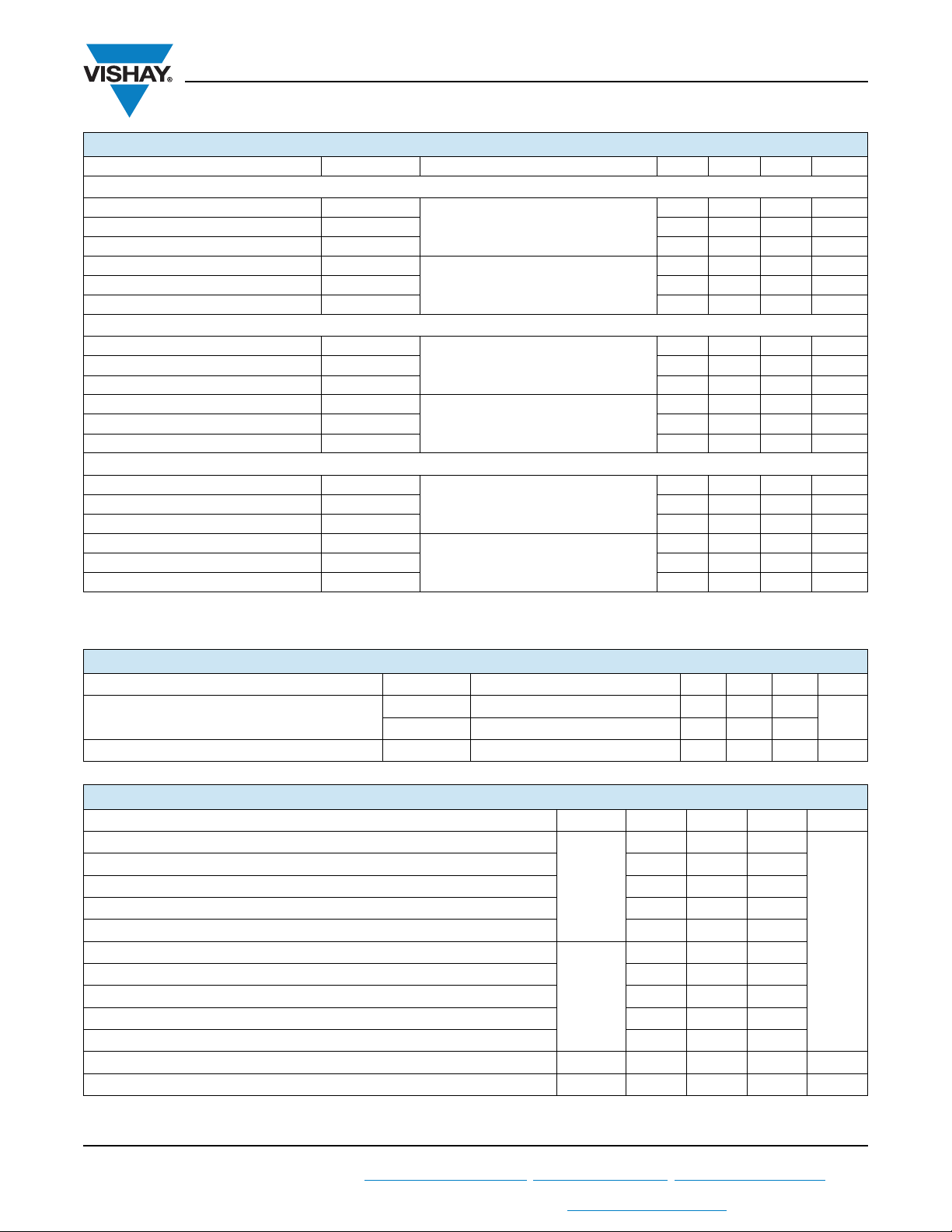
VS-EMF050J60U
www.vishay.com
SWITCHING CHARACTERISTICS (TJ = 25 °C unless otherwise noted)
PARAMETER SYMBOL TEST CONDITIONS MIN. TYP. MAX. UNITS
D1 - D2 CLAMPING DIODE
Diode reverse recovery time t
Diode peak reverse current I
Diode recovery charge Q
Diode reverse recovery time t
Diode peak reverse current I
Diode recovery charge Q
D3 - D4 AP DIODE
Diode reverse recovery time t
Diode peak reverse current I
Diode recovery charge Q
Diode reverse recovery time t
Diode peak reverse current I
Diode recovery charge Q
D5 - D6 AP DIODE
Diode reverse recovery time t
Diode peak reverse current I
Diode recovery charge Q
Diode reverse recovery time t
Diode peak reverse current I
Diode recovery charge Q
Note
(1)
Energy losses include “tail” and diode reverse recovery.
rr
rr
rr
rr
rr
rr
rr
rr
rr
rr
rr
rr
rr
rr
rr
rr
rr
rr
VR = 200 V
I
= 30 A
F
dl/dt = 500 A/μs
VR = 200 V
I
= 30 A
F
dl/dt = 500 A/μs, T
VR = 400 V
I
= 50 A
F
dl/dt = 500 A/μs
VR = 400 V
I
= 50 A
F
dl/dt = 500 A/μs, T
VR = 200 V
= 30 A
I
F
dl/dt = 500 A/μs
VR = 200 V
= 30 A
I
F
dl/dt = 500 A/μs, T
= 125 °C
J
= 125 °C
J
= 125 °C
J
Vishay Semiconductors
-5080ns
-7.511 A
- 185 440 nC
- 107 147 ns
-1822A
- 955 1620 nC
- 114 150 ns
-2125A
- 1200 1875 nC
- 170 210 ns
-2832A
- 2160 3360 nC
-4677ns
-711A
- 161 423 nC
- 106 138 ns
-1722A
- 900 1518 nC
THERMISTOR ELECTRICAL CHARACTERISTICS (TJ = 25 °C unless otherwise noted)
PARAMETER SYMBOL TEST CONDITIONS MIN. TYP. MAX. UNITS
R
Resistance
25
R
100
B value B T
TJ = 100 °C 468 493 518
= 25 °C/TJ = 50 °C 3206 3375 3544 K
J
4500 5000 5500
THERMAL AND MECHANICAL SPECIFICATIONS
PARAMETER SYMBOL MIN. TYP. MAX. UNITS
Q1 - Q4 IGBT - Junction to case thermal resistance (per switch)
Q2 - Q3 IGBT - Junction to case thermal resistance (per switch) - - 0.37
D1 - D2 Clamping diode - Junction to case thermal resistance (per diode) - - 0.83
R
thJC
D3 - D4 AP diode - Junction to case thermal resistance (per diode) - - 0.71
D5 - D6 AP diode - Junction to case thermal resistance (per diode) - - 1.3
Q1 - Q4 IGBT - Case to sink thermal resistance (per switch)
Q2 - Q3 IGBT - Case to sink thermal resistance (per switch) - 0.31 -
D1 - D2 Clamping diode - Case to sink thermal resistance (per diode) - 0.51 -
R
thCS
(1)
D3 - D4 AP diode - Case to sink thermal resistance (per diode) - 0.41 -
D5 - D6 AP diode - Case to sink thermal resistance (per diode) - 0.62 -
Mounting torque (M4) -23Nm
Weight -39- g
Note
(1)
Mounting surface flat, smooth, and greased
Revision: 09-Dec-11
For technical questions within your region: [email protected]
5
THIS DOCUMENT IS SUBJECT TO CHANGE WITHOUT NOTICE. THE PRODUCTS DESCRIBED HEREIN AND THIS DOCUMENT
ARE SUBJECT TO SPECIFIC DISCLAIMERS, SET FORTH AT www.vishay.com/doc?91000
- - 0.37
-0.31-
Document Number: 93494
°C/W
Page 7

www.vishay.com
V
CE
(V)
TJ (°C)
10 16060 110
0.5
1.0
1.5
2.0
2.5
3.0
3.5
93494_04
4.0
100 A
50 A
27 A
VGE = 15 V
I
CE
(A)
VGE (V)
387456
0
93494_05
100
30
40
10
50
60
20
80
90
70
TJ = 25 °C
VCE = 20 V
TJ = 125 °C
100
VGE = 15 V
90
80
70
60
50
(A)
C
I
40
30
20
10
0
0 1.5 3.01.0 2.50.5 2.0 3.5
93494_01
Fig. 1 - Typical Q1 - Q4 IGBT Output Characteristics
100
TJ = 125 °C
90
80
70
60
50
(A)
C
I
40
30
20
10
0
0 1.5 2.5 3.0 3.50.5 1.0 2.0 4.0
93494_02
Fig. 2 - Typical Q1 - Q4 IGBT Output Characteristics
TJ = 125 °C
TJ = 25 °C
VCE (V)
VCE (V)
TJ = 150 °C
VGE = 8 V
= 10 V
V
GE
= 12 V
V
GE
= 15 V
V
GE
= 18 V
V
GE
VS-EMF050J60U
Vishay Semiconductors
Fig. 4 - Typical Q1 - Q4 IGBT Collector to Emitter Voltage vs.
Junction Temperature
Fig. 5 - Typical Q1 - Q4 IGBT Transfer Characteristics
160
140
120
100
80
60
40
20
Allowable Case Temperature (°C)
0
0
93494_03
IC - Continuous Collector Current (A)
Fig. 3 - Maximum DC Q1 - Q4 IGBT Collector Current vs.
Case Temperature per Junction
Revision: 09-Dec-11
For technical questions within your region: [email protected]
THIS DOCUMENT IS SUBJECT TO CHANGE WITHOUT NOTICE. THE PRODUCTS DESCRIBED HEREIN AND THIS DOCUMENT
4.5
4.0
DC
3.5
TJ = 25 °C
(V)
geth
V
3.0
2.5
93494_06
2.0
01.00.20.1 0.3 0.5 0.7 0.90.4 0.6 0.8
IC (mA)
80604020
100
Fig. 6 - Typical Q1 - Q4 IGBT Gate Threshold Voltage
6
ARE SUBJECT TO SPECIFIC DISCLAIMERS, SET FORTH AT www.vishay.com/doc?91000
TJ = 125 °C
Document Number: 93494
Page 8

www.vishay.com
I
C
(A)
VCE (V)
1 10 100 1000
0.01
0.1
1
93494_07
1000
10
100
Fig. 7 - Q1 - Q4 IGBT Reverse Bias SOA
T
= 150 °C, VGE = 15 V, Rg = 22
J
VS-EMF050J60U
Vishay Semiconductors
160
140
120
100
80
60
40
20
Allowable Case Temperature (°C)
0
0
93494_10
IF - Continuous Forward Current (A)
Fig. 10 - Maximum DC D5 - D6 Antiparallel Diode
Forward Current vs. Case Temperature per Junction
DC
2515105353020 40 45
50
1
(mA)
CES
I
0.0001
93494_08
0.1
0.01
0.001
100 600200 300 400 500
125 °C
25 °C
V
CES
(V)
Fig. 8 - Typical Q1 - Q4 IGBT Zero Gate Voltage Collector Current
100
90
80
70
60
50
(A)
F
I
40
30
20
10
0
03.00.5 1.0 1.5 2.0 2.5
93494_09
Fig. 9 - Typical D5 - D6 Antiparallel Diode Forward Characteristics
TJ = 125 °C
TJ = 25 °C
VFM (V)
1.8
1.6
1.4
1.2
1.0
E
off
E
on
IC (A)
Energy (mJ)
93494_11
0.8
0.6
0.4
0.2
0
10 20 50 7030 60 8040 90
Fig. 11 - Typical Q1 - Q4 IGBT Energy Loss vs. I
(with Freewheeling D1 - D2 Clamping Diode)
V
= 400 V, Rg = 4.7 , VGE = 15 V, L = 500 μH
CC
1000
t
d(off)
t
d(on)
Switching Time (ns)
93494_12
100
10
t
f
t
r
10 20 30 806040 50 70 90
IC (A)
Fig. 12 - Typical Q1 - Q4 IGBT Switching Time vs. I
(with Freewheeling D1 - D2 Clamping Diode)
T
= 125 °C, VCC = 400 V, Rg = 4.7 , VGE = 15 V, L = 500 μH
J
C
C
Revision: 09-Dec-11
For technical questions within your region: [email protected]
THIS DOCUMENT IS SUBJECT TO CHANGE WITHOUT NOTICE. THE PRODUCTS DESCRIBED HEREIN AND THIS DOCUMENT
ARE SUBJECT TO SPECIFIC DISCLAIMERS, SET FORTH AT www.vishay.com/doc?91000
7
Document Number: 93494
Page 9

www.vishay.com
I
rr
(A)
dIF/dt (A/μs)
100 200 300 400
93494_14
500
1
21
7
13
3
9
17
15
11
19
5
125 °C
25 °C
Q
rr
(nC)
dIF/dt (A/μs)
100 200 300 400
93494_15
500
0
200
100
1100
1000
400
600
800
500
700
900
300
125 °C
25 °C
160
150
140
130
120
110
100
(ns)
rr
t
90
80
70
60
50
40
100 200 300 400
93494_13
Fig. 13 - Typical D5 - D6 Antiparallel Diode Reverse
125 °C
25 °C
dIF/dt (A/μs)
Recovery Time vs. dI
V
= 200 V, IF = 30 A
R
F
/dt
500
VS-EMF050J60U
Vishay Semiconductors
Fig. 14 - Typical D5 - D6 Antiparallel Diode Reverse
Recovery Current vs. dI
V
= 200 V, IF = 30 A
R
/dt
F
1
0.1
0.01
- Thermal Impedance
Junction to Case (°C/W)
thJC
Revision: 09-Dec-11
Z
0.001
0.00001
93494_16
For technical questions within your region: [email protected]
THIS DOCUMENT IS SUBJECT TO CHANGE WITHOUT NOTICE. THE PRODUCTS DESCRIBED HEREIN AND THIS DOCUMENT
Fig. 15 - Typical D5 - D6 Antiparallel Diode Reverse Recovery Charge vs. dI
V
= 200 V, IF = 30 A
R
D = 0.50
D = 0.20
D = 0.10
D = 0.05
D = 0.02
D = 0.01
DC
0.0001 0.001 0.01 0.1 1
t1 - Rectangular Pulse Duration (s)
Fig. 16 - Maximum Thermal Impedance Z
Characteristics (Q1 - Q4 IGBT)
thJC
8
ARE SUBJECT TO SPECIFIC DISCLAIMERS, SET FORTH AT www.vishay.com/doc?91000
/dt
F
10
Document Number: 93494
Page 10

www.vishay.com
Allowable Case Temperature (°C)
IC - Continuous Collector Current (A)
80604020
100
0
100
160
0
40
60
140
80
120
20
93494_20
DC
V
CE
(V)
TJ (°C)
10 16060 110
1.0
1.5
2.0
2.5
3.0
3.5
93494_21
4.0
100 A
50 A
27 A
VGE = 15 V
10
1
VS-EMF050J60U
Vishay Semiconductors
0.1
- Thermal Impedance
0.01
Junction to Case (°C/W)
thJC
Z
0.001
0.00001
93494_17
0.0001 0.001 0.01 0.1 1
Fig. 17 - Maximum Thermal Impedance Z
100
VGE = 15 V
90
80
70
(A)
C
I
93494_18
60
50
40
30
20
10
0
TJ = 125 °C
0 1.5 3.01.0 2.50.5 2.0 3.5
TJ = 150 °C
TJ = 25 °C
VCE (V)
Fig. 18 - Typical Q2 - Q3 IGBT Output Characteristics
D = 0.50
D = 0.20
D = 0.10
D = 0.05
D = 0.02
D = 0.01
DC
t1 - Rectangular Pulse Duration (s)
Characteristics (D5 - D6 Antiparallel Diode)
thJC
Fig. 20 - Maximum DC Q2 - Q3 IGBT Collector Current vs.
10
Case Temperature per Junction
100
TJ = 125 °C
90
80
70
60
50
(A)
C
I
40
30
20
10
93494_19
Revision: 09-Dec-11
0
0 1.5 2.5 3.0 3.50.5 1.0 2.0 4.0
Fig. 19 - Typical Q2 - Q3 IGBT Output Characteristics
For technical questions within your region: [email protected]
THIS DOCUMENT IS SUBJECT TO CHANGE WITHOUT NOTICE. THE PRODUCTS DESCRIBED HEREIN AND THIS DOCUMENT
VGE = 9 V
= 12 V
V
GE
= 15 V
V
GE
= 18 V
V
GE
VCE (V)
Fig. 21 - Typical Q2 - Q3 IGBT Collector to Emitter Voltage vs.
Junction Temperature
9
ARE SUBJECT TO SPECIFIC DISCLAIMERS, SET FORTH AT www.vishay.com/doc?91000
Document Number: 93494
Page 11

www.vishay.com
I
CE
(A)
VGE (V)
498567
0
93494_22
100
30
40
10
50
60
20
80
90
70
VCE = 20 V
TJ = 25 °C
TJ = 125 °C
I
C
(A)
VCE (V)
1 10 100 1000
0.01
0.1
1
93494_24
1000
10
100
I
CES
(mA)
V
CES
(V)
100 900200 300 400 500 600 700 800
0.0001
93494_25
10
1
0.1
0.01
0.001
125 °C
25 °C
VS-EMF050J60U
Vishay Semiconductors
Fig. 22 - Typical Q1 - Q4 IGBT Transfer Characteristics
5.5
(V)
geth
V
93494_23
5.0
4.5
4.0
3.5
3.0
2.5
2.0
1.5
01.00.20.1 0.3 0.5 0.7 0.90.4 0.6 0.8
TJ = 25 °C
Fig. 23 - Typical Q2 - Q3 IGBT Gate Threshold Voltage
Revision: 09-Dec-11
Fig. 24 - Q2 - Q3 IGBT Reverse Bias SOA
T
= 150 °C, VGE = 15 V, Rg = 22
J
For technical questions within your region: [email protected]
THIS DOCUMENT IS SUBJECT TO CHANGE WITHOUT NOTICE. THE PRODUCTS DESCRIBED HEREIN AND THIS DOCUMENT
ARE SUBJECT TO SPECIFIC DISCLAIMERS, SET FORTH AT www.vishay.com/doc?91000
TJ = 125 °C
IC (mA)
Fig. 25 - Typical Q2 - Q3 IGBT Zero Gate Voltage Collector Current
100
90
TJ = 25 °C
TJ = 125 °C
VFM (V)
(A)
F
I
93494_26
80
70
60
50
40
30
20
10
0
04.53.0 3.5 4.00.5 1.0 1.5 2.0 2.5
Fig. 26 - Typical D3 - D4 Antiparallel Diode Forward Characteristics
160
140
120
100
80
60
40
20
Allowable Case Temperature (°C)
93494_27
0
0
IF - Continuous Forward Current (A)
2515105353020 40 45
DC
Fig. 27 - Maximum DC D3 - D4 Antiparallel Diode
Forward Current vs. Case Temperature per Junction
10
Document Number: 93494
6050 55
Page 12

www.vishay.com
t
rr
(ns)
dIF/dt (A/μs)
100 200 300 400
93494_30
500
100
280
140
200
240
180
120
160
220
260
125 °C
25 °C
I
rr
(A)
dIF/dt (A/μs)
100 200 300 400
93494_31
500
4
32
16
28
8
20
24
12
125 °C
25 °C
Q
rr
(nC)
dIF/dt (A/μs)
100 200 300 400
93494_32
500
500
2500
1000
1500
2000
1250
1750
2250
750
125 °C
25 °C
4.2
3.8
3.4
3.0
2.6
2.2
1.8
Energy (mJ)
1.4
1.0
0.6
0.2
10 20 50 7030 60 8040 90
93494_28
Fig. 28 - Typical Q2 - Q3 IGBT Energy Loss vs. I
(with Freewheeling D2 - D3 AP Diode)
V
= 720 V, Rg = 4.7 , VGE = 15 V, L = 500 μH
CC
1000
E
off
IC (A)
VS-EMF050J60U
Vishay Semiconductors
E
on
C
Fig. 30 - Typical D3 - D4 Antiparallel Diode Reverse
Recovery Time vs. dI
V
= 400 V, IF = 50 A
R
/dt
F
t
Switching Time (ns)
93494_29
f
t
100
10
10 20 30 806040 50 70 90
d(on)
t
d(off)
t
r
IC (A)
Fig. 29 - Typical Q2 - Q3 IGBT Switching Time vs. I
(with Freewheeling D2 - D3 AP Diode)
T
= 125 °C, VCC = 720 V, Rg = 4.7 , VGE = 15 V, L = 500 μH
J
C
Fig. 31 - Typical D3 - D4 Antiparallel Diode Reverse
Recovery Current vs. dI
V
= 400 V, IF = 50 A
R
/dt
F
Revision: 09-Dec-11
For technical questions within your region: [email protected]
THIS DOCUMENT IS SUBJECT TO CHANGE WITHOUT NOTICE. THE PRODUCTS DESCRIBED HEREIN AND THIS DOCUMENT
Fig. 32 - Typical D3 - D4 Antiparallel Diode Reverse Recovery Charge vs. dI
V
= 400 V, IF = 50 A
R
/dt
F
11
ARE SUBJECT TO SPECIFIC DISCLAIMERS, SET FORTH AT www.vishay.com/doc?91000
Document Number: 93494
Page 13

www.vishay.com
1
0.1
0.01
- Thermal Impedance
Junction to Case (°C/W)
thJC
Z
0.001
0.00001
93494_33
10
1
D = 0.50
D = 0.20
D = 0.10
D = 0.05
D = 0.02
D = 0.01
DC
0.0001 0.001 0.01 0.1 1
t1 - Rectangular Pulse Duration (s)
Fig. 33 - Maximum Thermal Impedance Z
Characteristics (Q2 - Q3 IGBT)
thJC
VS-EMF050J60U
Vishay Semiconductors
10
(A)
F
I
93494_35
0.1
- Thermal Impedance
0.01
Junction to Case (°C/W)
thJC
Z
0.001
0.00001
93494_34
0.0001 0.001 0.01 0.1 1
Fig. 34 - Maximum Thermal Impedance Z
100
90
80
70
60
50
40
30
20
10
0
01.51.0 2.50.5 2.0 3.0
TJ = 125 °C
TJ = 25 °C
VFM (V)
t1 - Rectangular Pulse Duration (s)
D = 0.50
D = 0.20
D = 0.10
D = 0.05
D = 0.02
D = 0.01
DC
Characteristics (D3 - D4 Antiparallel Diode)
thJC
160
140
120
100
80
60
40
20
Allowable Case Temperature (°C)
0
0
93494_36
IF - Continuous Forward Current (A)
DC
10
5030 60402010
70
Fig. 35 - Typical D1 - D2 Clamping Diode Forward Characteristics Fig. 36 - Maximum DC D1 - D2 Clamping Diode
Forward Current vs. Case Temperature per Junction
Revision: 09-Dec-11
For technical questions within your region: [email protected]
12
Document Number: 93494
THIS DOCUMENT IS SUBJECT TO CHANGE WITHOUT NOTICE. THE PRODUCTS DESCRIBED HEREIN AND THIS DOCUMENT
ARE SUBJECT TO SPECIFIC DISCLAIMERS, SET FORTH AT www.vishay.com/doc?91000
Page 14

www.vishay.com
I
R
(mA)
VR (V)
100 200 300 400 500 600
0.0001
0.001
0.01
0.1
1
10
93494_37
125 °C
25 °C
I
rr
(A)
dIF/dt (A/μs)
100 200 300 400
93494_39
500
1
21
7
13
3
9
17
15
11
19
5
125 °C
25 °C
Q
rr
(nC)
dIF/dt (A/μs)
100 200 300 400
93494_40
500
0
1000
200
400
600
300
500
700
900
800
100
125 °C
25 °C
VS-EMF050J60U
Vishay Semiconductors
Fig. 37 - Typical D1 - D2 Clamping Diode
Reverse Leakage Current
160
140
125 °C
120
100
(ns)
rr
t
80
25 °C
60
40
100 200 300 400
93494_38
dIF/dt (A/μs)
Fig. 38 - Typical D1 - D2 Clamping Diode Reverse
Recovery Time vs. dI
V
= 200 V, IF = 30 A
R
10
1
Fig. 39 - Typical D1 - D2 Clamping Diode Reverse
/dt
F
500
Recovery Current vs. dI
V
= 200 V, IF = 30 A
R
Fig. 40 - Typical D1 - D2 Clamping Diode Reverse
/dt
F
Recovery Charge vs. dI
V
= 200 V, IF = 30 A
R
/dt
F
0.1
- Thermal Impedance
0.01
Junction to Case (°C/W)
Revision: 09-Dec-11
thJC
Z
0.001
0.00001
93494_41
Fig. 41 - Maximum Thermal Impedance Z
For technical questions within your region: [email protected]
THIS DOCUMENT IS SUBJECT TO CHANGE WITHOUT NOTICE. THE PRODUCTS DESCRIBED HEREIN AND THIS DOCUMENT
ARE SUBJECT TO SPECIFIC DISCLAIMERS, SET FORTH AT www.vishay.com/doc?91000
D = 0.50
D = 0.20
D = 0.10
D = 0.05
D = 0.02
D = 0.01
DC
0.0001 0.001 0.01 0.1 1
t1 - Rectangular Pulse Duration (s)
Characteristics (D1 - D2 Clamping Diode)
thJC
13
10
Document Number: 93494
Page 15

www.vishay.com
1 - Vishay Semiconductors product
2 - Package indicator (EM = EMIPAK2)
3 - Circuit configuration (F = 3-levels half-bridge inverter stage)
4 - Current rating (050 = 50 A)
5 - Die technology (J = Warp2 IGBT)
6 - Voltage rating (60 = 600 V)
7 - U = Ultrafast
Device code
51 32 4 6 7
VS- EM F 050 J 60 U
ORDERING INFORMATION TABLE
TYPICAL CONNECTION
VS-EMF050J60U
Vishay Semiconductors
Note
• Please refer to lead assignment for correct pin configuration. This diagram shows electrical connections only.
Revision: 09-Dec-11
For technical questions within your region: [email protected]
THIS DOCUMENT IS SUBJECT TO CHANGE WITHOUT NOTICE. THE PRODUCTS DESCRIBED HEREIN AND THIS DOCUMENT
ARE SUBJECT TO SPECIFIC DISCLAIMERS, SET FORTH AT www.vishay.com/doc?91000
14
Document Number: 93494
Page 16

www.vishay.com
+ 400 V
17
35
MID
14
15
VMID
29
30
36
Q1
Q2
Q3
Q4
Th
D5
D3
D4
D6
D2
D1
- 400 V
26
27
Inv_Drv1
33
1
5
9
6
11
Inv_Drv2
8
4
Inv_Drv3
3
2
Inv_Drv3
23
24
33
11
5612
14 15
35
17
26
27
2324
3036
9
4
8
3
29
CIRCUIT CONFIGURATION
VS-EMF050J60U
Vishay Semiconductors
PACKAGE
Dimensions www.vishay.com/doc?95436
Revision: 09-Dec-11
For technical questions within your region: [email protected]
THIS DOCUMENT IS SUBJECT TO CHANGE WITHOUT NOTICE. THE PRODUCTS DESCRIBED HEREIN AND THIS DOCUMENT
ARE SUBJECT TO SPECIFIC DISCLAIMERS, SET FORTH AT www.vishay.com/doc?91000
LINKS TO RELATED DOCUMENTS
15
Document Number: 93494
Page 17

DIMENSIONS in millimeters
5.1
12.7
8.9
10.2
7.6
7.6
11.4
55 ± 0.3
15.2 14
58 ± 0.3
40.6
1.3
2.6
1.3
5.1
3.8
3.8
10.1
16.5
62 ± 0.3
53
23.8
23
41.5
Ø 5
Ø 2
Ø 4.3
Ø 1 ± 0.1
20.5 ± 1
17 ± 1
12
M4
Ø 0.4
6.4
16.8
145°
62 ± 0.3
39 ± 0.3
3 ref.
0.1
20.5 ± 1
24.1
20.3
16.5
12.7
8.9
2.5
6.3
11.4
20.3
24.1
13.3
12.1
9.59.5
5.7
7
3.2
1.9
7
10.8
15.9
1.9
5.7
8.3
12.1
15.9
Pins position
with tolerance
Front view
FF
Top view
Flat metal plate or
with optional M4 thread
Detail “A” Scale 10:1
Ceramic gap
Detail “A”
Side view
Outline Dimensions
Vishay Semiconductors
EMIPAK2
www.vishay.com
Page 18

Legal Disclaimer Notice
www.vishay.com
Vishay
Disclaimer
ALL PRODUCT, PRODUCT SPECIFICATIONS AND DATA ARE SUBJECT TO CHANGE WITHOUT NOTICE TO IMPROVE
RELIABILITY, FUNCTION OR DESIGN OR OTHERWISE.
Vishay Intertechnology, Inc., its affiliates, agents, and employees, and all persons acting on its or their behalf (collectively,
“Vishay”), disclaim any and all liability for any errors, inaccuracies or incompleteness contained in any datasheet or in any other
disclosure relating to any product.
Vishay makes no warranty, representation or guarantee regarding the suitability of the products for any particular purpose or
the continuing production of any product. To the maximum extent permitted by applicable law, Vishay disclaims (i) any and all
liability arising out of the application or use of any product, (ii) any and all liability, including without limitation special,
consequential or incidental damages, and (iii) any and all implied warranties, including warranties of fitness for particular
purpose, non-infringement and merchantability.
Statements regarding the suitability of products for certain types of applications are based on Vishay’s knowledge of typical
requirements that are often placed on Vishay products in generic applications. Such statements are not binding statements
about the suitability of products for a particular application. It is the customer’s responsibility to validate that a particular
product with the properties described in the product specification is suitable for use in a particular application. Parameters
provided in datasheets and/or specifications may vary in different applications and performance may vary over time. All
operating parameters, including typical parameters, must be validated for each customer application by the customer’s
technical experts. Product specifications do not expand or otherwise modify Vishay’s terms and conditions of purchase,
including but not limited to the warranty expressed therein.
Except as expressly indicated in writing, Vishay products are not designed for use in medical, life-saving, or life-sustaining
applications or for any other application in which the failure of the Vishay product could result in personal injury or death.
Customers using or selling Vishay products not expressly indicated for use in such applications do so at their own risk. Please
contact authorized Vishay personnel to obtain written terms and conditions regarding products designed for such applications.
No license, express or implied, by estoppel or otherwise, to any intellectual property rights is granted by this document or by
any conduct of Vishay. Product names and markings noted herein may be trademarks of their respective owners.
Material Category Policy
Vishay Intertechnology, Inc. hereby certifies that all its products that are identified as RoHS-Compliant fulfill the
definitions and restrictions defined under Directive 2011/65/EU of The European Parliament and of the Council
of June 8, 2011 on the restriction of the use of certain hazardous substances in electrical and electronic equipment
(EEE) - recast, unless otherwise specified as non-compliant.
Please note that some Vishay documentation may still make reference to RoHS Directive 2002/95/EC. We confirm that
all the products identified as being compliant to Directive 2002/95/EC conform to Directive 2011/65/EU.
Vishay Intertechnology, Inc. hereby certifies that all its products that are identified as Halogen-Free follow Halogen-Free
requirements as per JEDEC JS709A standards. Please note that some Vishay documentation may still make reference
to the IEC 61249-2-21 definition. We confirm that all the products identified as being compliant to IEC 61249-2-21
conform to JEDEC JS709A standards.
Revision: 02-Oct-12
1
Document Number: 91000
 Loading...