

Page 1

ELAN MICROELECTRONICS CORPORATION
EM92547A/B/D
CALLER ID FSK DECODER
ELAN MICROELECTRONICS CORP.
Office :
6-F1.,42, Sec.2, Chung Shaan N.
Road.,
Taipei, Taiwan, R.O.C.
TEL : (02) 5628813 EXT.686,687;5223065
FAX : (02) 5516348
TELEX : 21540 HTC, 22486 EHSIN
7F-1, No. 9 Prosperity 1st Rd.
Science-Based Industrial Park. Hsin Chu
City.
Taiwan, R.O.C.
TEL : (03) 5787505
FAX : (03) 5779095
Publication Release Date :
Agent :
Page 2

EM92547A/B/D
CALLER ID FSK DECODER
________________________________________________________________________________________________________________________________________________________
* This specification are subject to be changed without notice. 1998
~ 1 ~
General Description
The EM92547 is a single-chip CMOS receiver IC designed to work in telephone
equipment incorporating Calling Number Delivery (CND) capabilities. CND capabilities
can be add to equipment such as telephone, adjunct units, answering machines, and
facsimile machines, by using the EM92547 and any standard microcontroller IC. The
EM92547 detects and qualifies the incoming ring signal, performs an energy detect on
incoming FSK signal, and demodulates the FSK data in accordance with BELL 202
standards. Integrating the above functions the equipment manufacturer a cost-effective
means of implementing CND capabilities into their products.
Features
• Compatible with Bellcore GR-30-CORE (formerly as TR-NWT-000030).
• Compatible with British Telecom (BT) SIN227 & SIN242.
• FSK demodulator for Bell 202 and ITU-T V.23 (formerly as CCITT V.23)
• On-chip ring detector
• Ring detect and carrier detect output for MCU interrupt
• Power down mode operation
• On-chip band pass filter
• FSK demodulation with energy detect
• High input sensitivity
• Low current consumption in power down mode
• Single supply from 3.5V to 6V
• Clock Frequencies: 3.58MHz or 455KHz for EM92547A
: 3.58MHz for EM92547B/D
• Package series --- 16-pin DIP or 16-pin SOP (150 mil)
EM92547BP/DP for 16-pin DIP
EM92547BN/DN for 16-pin SOP (150 mil)
Application
•
adjunct units
• answering machines
• feature phones
• fax machines
• computer interface products
Page 3
EM92547A/B/D
CALLER ID FSK DECODER
________________________________________________________________________________________________________________________________________________________
* This specification are subject to be changed without notice. 1998
~ 2 ~
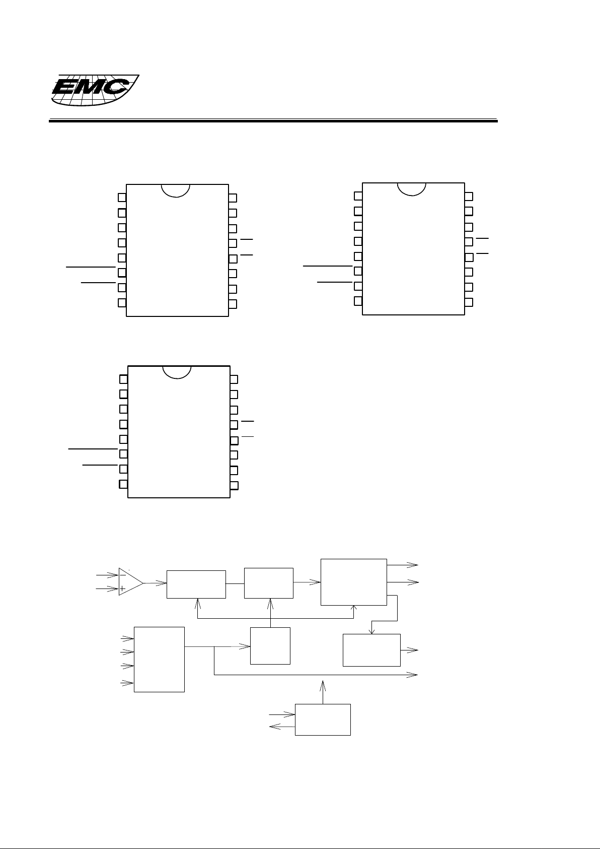
Pin Assignments
Functional Block Diagram
TIP
RING DET2
PWR UP
SHORTDATA
CD
CLK SELECT
14
13
12
11
1
2
3
4
5
6
7
VDD
10
RING
RING DET1
OSCOUT
OSCIN
RING TIME
RD
NC
DVSS
8
9
DATA OUT
EM92547A
TIP
RING DET2
PWR UP
NC
CD
NC
1
2
3
4
5
6
7
VDD
RING
RING DET1
OSCOUT
OSCIN
RING TIME
RD
NC
DVSS 8
DATA OUT
EM92547B
15
16
14
13
12
11
10
9
15
16
TIP
RING DET2
PWR UP
CD
NC
1
2
3
4
5
6
7
VDD
RING
RING DET1
OSCOUT
OSCIN
RING TIME
RD
NC
DVSS 8
DATA OUT
EM92547D
14
13
12
11
10
9
15
16
SHORTDATA
Data Re-
timing
Ring
Det.
Circuit
Ring det1
Ring det2
Tip
Ring
Power
Up
FSK
Demod
Data Valid
Energy Det
Circuit
DATAOUT
/CD
Clock
OSCIN
OSCOUT
/RD
/Ring Time
/PWR UP
Band Pass
Filter
SHORTDATA
Page 4
EM92547A/B/D
CALLER ID FSK DECODER
________________________________________________________________________________________________________________________________________________________
* This specification are subject to be changed without notice. 1998
~ 3 ~
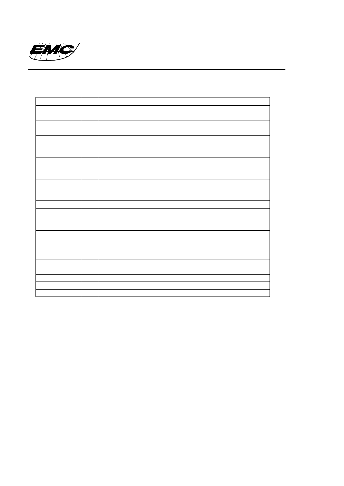
Pin Descriptions
Symbol I/O Function
TIP I This input is connected to the tip line of the twisted pair.
RING I This input is connected to the ring line of the twisted pair.
RING DET1 I This input is coupled to one end of the line through an attenuation
network. It is used to detect the occurrence of a valid ring signal.
RING DET2 I This input is coupled to the other end of the line through an
attenuation network.
SHORTDATA O Data output pin without preamble message.
/RING TIME O A RC network should be connected to this pin. The RC time
constant is chosen to hold this pin voltage below 2.2V between
the peaks of the ringing signal.
/PWR UP I This active low input sets the chip into power up. When high, the
chip is put into a power down mode in the absence of a ring
signal. In this mode, only the ring detect circuitry is active.
VSS Ground.
OSCOUT O This pin connects to the other side of the crystal oscillator.
OSCIN I This pin connects to 3.58MHz crystal oscillator or 455kHz
resonator. It can also be used as an external clock input.
CLK SELECT I A logic '1' on this pin to select 3.58MHz crystal oscillator, logic '0'
to select 455kHz resonator.
/RD O (ring detector)(active low)This output detects the presence of a
valid ring signal.
/CD O (carrier detect)(active low)This output indicates the presence of
in-band signals at the device input.
DATA OUT O The demodulated FSK data is output to this pin.
VDD Power Supply Voltage.
NC Non Connected.
Function Descriptions
The EM92547 is a CMOS device designed to support the Caller Number Deliver
feature, which is offered by the Regional Bell Operating Companies. The EM92547 CLID
comprises two paths: the signal path and the ring indicator path. The signal path consists of
an input differential buffer; a band pass filter, an FSK demodulator and a data valid with
carrier detect circuit. The ring detector path includes a clock generator, a ring detect circuit
and a power-up logic circuit.
In a typical application, the ring detector maintains the line continuously while all
other functions of the chip are inhibited. If a ring signal is sent, the ring detector wakes up
the oscillator and the main bias generator. This in turn activates the rest of the IC. Once
activated, a valid signal RI (ring indicator) is sent.
Page 5
EM92547A/B/D
CALLER ID FSK DECODER
________________________________________________________________________________________________________________________________________________________
* This specification are subject to be changed without notice. 1998
~ 4 ~
A /PWR UP input pin is provided to activate the chip regardless of the presence of a
power ring signal. If /PWR UP is sent high, the IC can still power itself up whenever it
detects a valid ring signal, but will back to its normal power-down mode after a time period.
The input buffer accepts a differential AC coupled input signal through the TIP and
RING input and feeds this signal to a band pass filter. Once the signal is filtered, the FSK
demodulator decodes the information and sents it to a post filter. The output data is then
made available at DATA OUT pin. This data, as sent by the central office, includes the
header information (alternate "1" and "0") and 150msec of marking which precedes the date,
time and calling number. If no data is present, the DATA OUT pin is held in a low state.
This is accomplished by a carrier detect circuit which determines if the in-band energy is
high enough. If the incoming signal is valid and thus the demodulated data is transferred to
DATA OUT pin. If it is not, then the FSK demodulator is blocked. This device uses a 3.58
MHz crystal or a 455KHz(for EM92547A only) resonator as a timing source for all the
internal blocks.
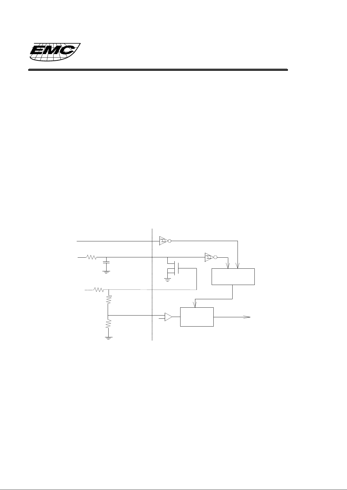
* Ring detect circuit
When Vdd is applied to the circuit, the RC network will charge cap C1 to Vdd
holding /RING TIME off. If /PWRUP is also held at Vdd, the whole circuit will be in a
power down mode, and will consume less than 1uA of supply current. The resistor network
R2 to R4 attenuates the incoming power ring applied to the top of R2. The values given
have been chosen to provide a sufficient voltage at pin3, to turn on the Schmitt trigger input.
When Vt+ of the Schmitt is exceeded, cap C1 will discharge. This will initialize a partial
power up, and enable the ring detect circuit.
The value of R1 and C1 must be chosen to hold the /RING TIME pin voltage below
the Vt+ of the Schmitt between the individual cycle of the power ring. The values shown
will work for ring frequencies of 15.3 Hz minimum.
/PWR UP
VDD
/Ring Time
Ring det1
Ring det2
1.2V
Ring
Counter
Power Up
Logic
C1
R3
R4
R1
R2
/RD
(form bridge)
Page 6
EM92547A/B/D
CALLER ID FSK DECODER
________________________________________________________________________________________________________________________________________________________
* This specification are subject to be changed without notice. 1998
~ 5 ~
With pin4 enabled, a portion of the power ring above 1.2V is fed to the ring counter
circuit. This circuit is a digital integrator. When the input signal at pin4 is above 1.2V,the
integrator is counting up at 800 Hz rate. Otherwise, counting down at 800Hz rate. A ring is
qualified when an internal count of binary 48 is reached and disqualified when an internal
count below binary 48.
Once the ring signal is qualified, the /RING INDICATOR will sent low. This can be
fed back to /PWR UP or can be used as an interrupt to an MCU. Once the /PWR UP pin is
below Vt-, the part will fully powered up, and ready to receive FSK. During this mode the
device current will increase to 3 mA typical.
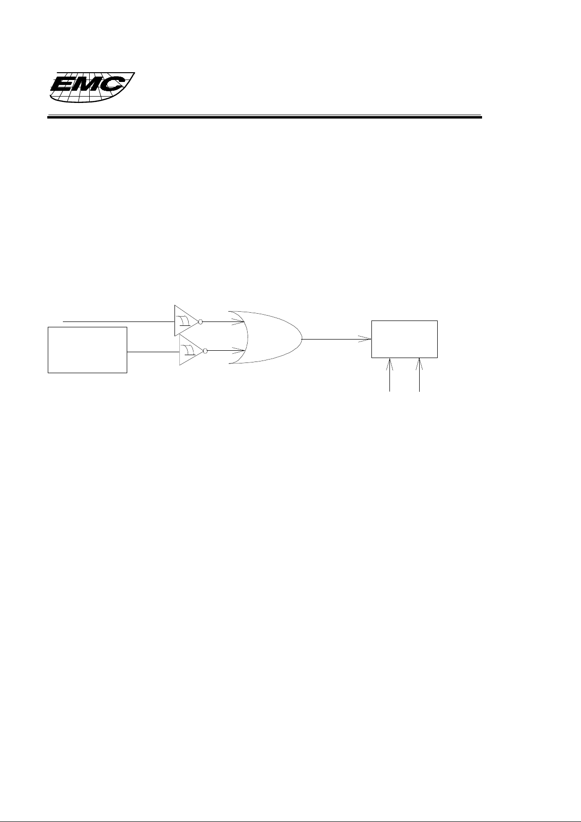
* power up circuit
The power up circuit accepts /PWR UP signal and /RD signal. In the power down
mode, if a ring signal is sent, the ring detector wakes up the oscillator and the main bias
generator. This in turn activates the IC. Once activated, a valid signal RD (ring detector) is
sent. Since no valid FSK single being detected, the whole IC will back to its power-down
mode after a period (default 3-second).
FSK data output(DATA OUT pin), FSK short data output(SHORTDATA) ,and FSK
carrier detect (/CD) :
As shown from functional block diagram, DATA OUT pin won’t have any FSK
decoding data until ‘Data Valid Energy Detect Circuit’ has detected enough energy and
timing (about 15ms) FSK signal coming. When this timing has been checked correctly,
open-drain carrier detect /CD pin will be pull low then DATA OUT pin will have decoding
data output. At this time, SHORTDATA pin will still not have any FSK decoding data until
enough energy and timing (about 12.5ms) FSK mark bits time have been checked. The
details timing about DATAOUT, SHORTDATA and /CD will be shown on Timing
Diagram for FSK timing.
RING
/RD
/PWR UP
WAKE UP
CLOCK
GEN
XTRL
DETECT
Page 7
EM92547A/B/D
CALLER ID FSK DECODER
________________________________________________________________________________________________________________________________________________________
* This specification are subject to be changed without notice. 1998
~ 6 ~
Absolute Maximum Ratings
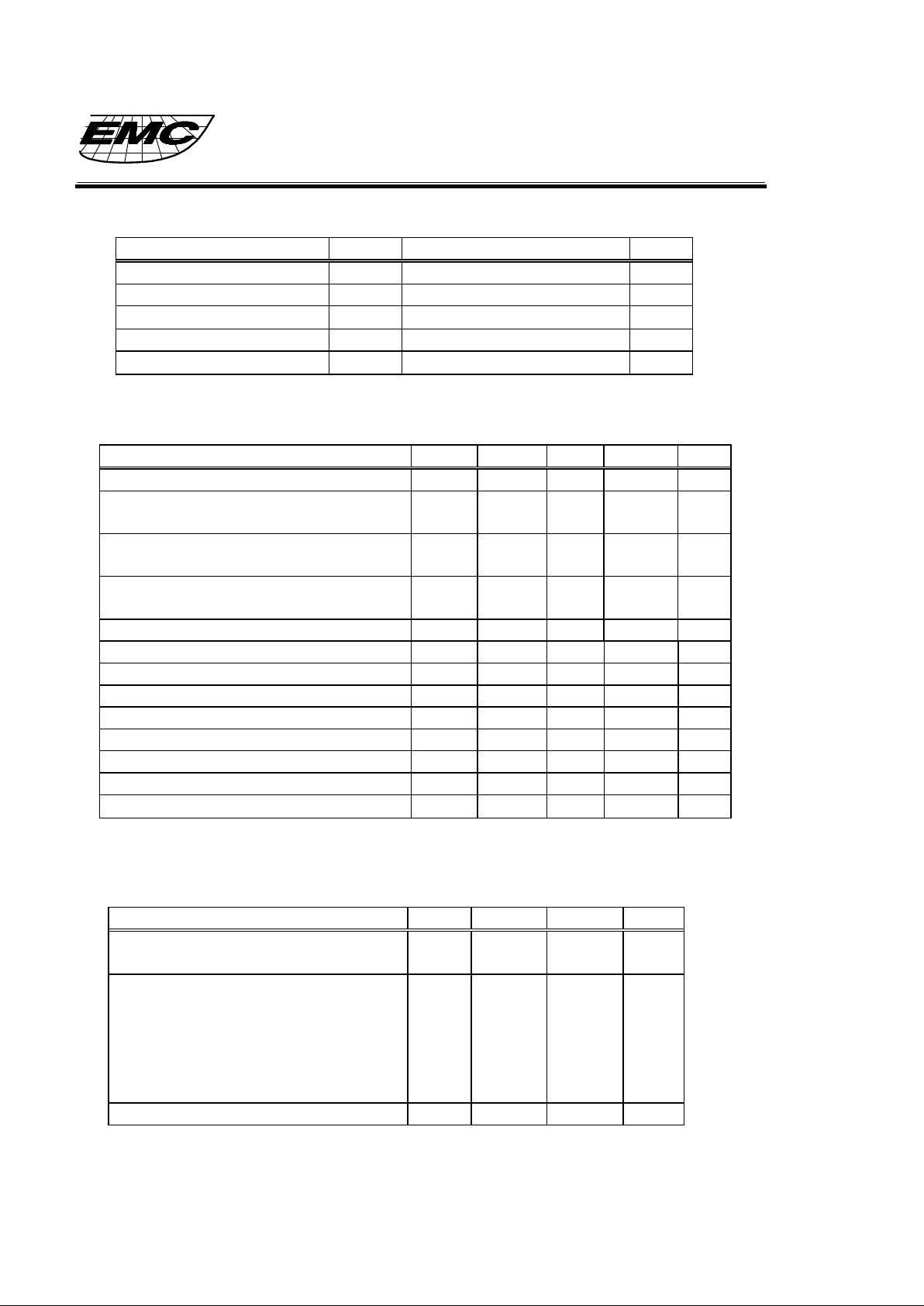
Rating Symbol Value Unit
DC supply voltage VDD -0.5.5 to 6 V
Input voltage VIN -0.5 to VDD +0.5 V
DC current drain per pin I
±10
mA
Power dissipation PD 20 mW
Operating temperature range TA 0 to 70
°C
DC Electrical Characteristic
(Referenced to VDD=5V VSS=0V)
Parameter Symbol Min. Typ. Max. unit
DC supply voltage VDD 3.5 5 5.5 V
Supply current(output pins unload) /pwr
up =1 Xtal=3.58MHz
IDD -- 3 5 mA
Supply current (output pins unload) /pwr
up =0 /ring time=0 Xtal=3.58MHz
IDD -- 3 5 mA
Standby current(output pins unload) /ring
time =1 /pwr up =1
Istby -- -- 1 uA
Input voltage '0' level Vil -- -- VDDx0.3 V
Input voltage '1' level Vih VDDx0.7 -- -- V
Output voltage high Ioh=0.16 mA Voh 2.5 -- -- V
Ouput voltage low Iol=2.0 mA Vol -- 0.3 0.4 V
Input leakage current Iin -- -- +/-1 uA
Input threshold voltage positive going Vt+ TBD 2.9 TBD V
Input threshold voltage negative going Vt- TBD 2.2 TBD V
Ring det2 threshold Rd2Vt TBD 1.2 TBD V
Tip/Ring input DC resistance Rin -- 500 --
kΩ
AC Electrical Characteristic
(VDD=+5V,TA=+25°C)
Characteristics Min. Typ. Max Unit
Input sensitivity TIP and RING
Pin1 and pin2 VDD=+5V
-35 -48 -- dBm
Band Pass FilterFrequence
response(relative to 1700Hz @ 0 dBm)
60Hz
550Hz
2700Hz
¡Ù3300Hz
--
--
--
--
-58
-3
-3
-30
--
--
--
--
Energy detect sensitivity -- -44 -- dBm
Page 8
EM92547A/B/D
CALLER ID FSK DECODER
________________________________________________________________________________________________________________________________________________________
* This specification are subject to be changed without notice. 1998
~ 7 ~
Timing Diagrams
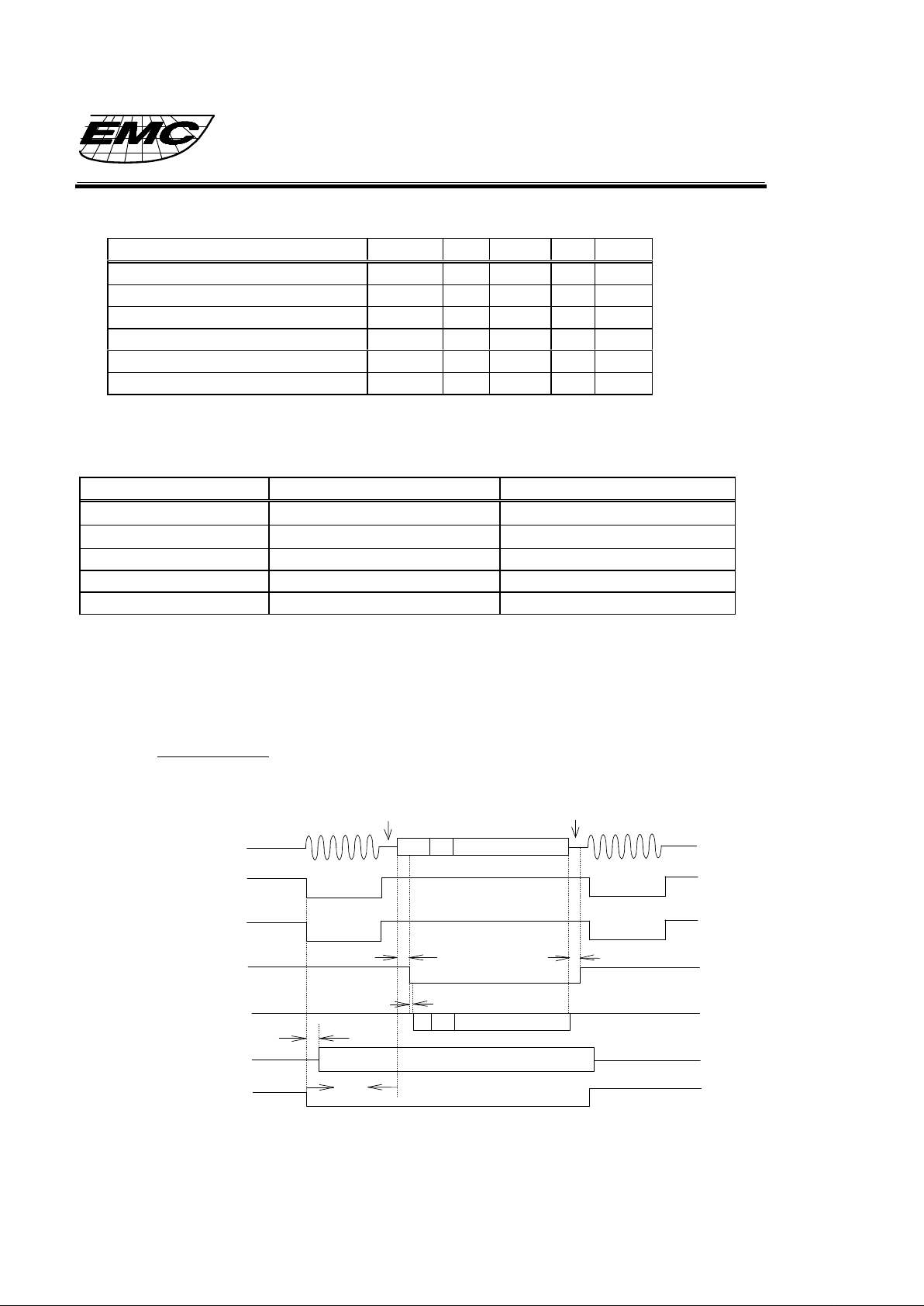
Description Symbol Min. Typ. Max. Unit
OSC start up TOSC -- 2 4 ms
Carrier detect low TCDL 10 15 20 ms
DATA OUT to Carrier det low TDOC -- 10 20 ns
SHORTDATA to mark det valid TSDV 10 12.5 15 Ms
Power up low to FSK(setup time) TSUP -- 15 20 ms
End of FSK to Carrier Detect high TCDH 25 30 35 ms
FSK format
There are some differences on signal spec. between Bell 202 and ITU-T V.23.
Item Bell 202 ITU-T V.23
Mark freq. (logic 1)
1200±1% 1300±1.5%
Space freq. (logic 0)
2200±1% 2100±1.5%
Transmission rate 1200 bps 1200 bps
Data format serial, asynchronous serial, asynchronous
Modulation type analog phase coherent FSK analog phase coherent FSK
FSK timing (‘CS’ –– Channel Seizure, ‘M’ –– Mark, FSK data –– FSK data signal)
1. DATA OUT timing
On-hook FSK :
TIP/RING
/CD
DATA OUT
OSC
FIRST RING
2 SECONDS
0.5 SEC
0.5 SEC
SECOND RING
2 SECONDS
DATA
T
CDL
/PWUP
3.58MHz
T
DOC
T
CDH
T
OSC
1
/RING TIME
/RD
T
SUP
CS M
FSK data
1010..
Page 9
EM92547A/B/D
CALLER ID FSK DECODER
________________________________________________________________________________________________________________________________________________________
* This specification are subject to be changed without notice. 1998
~ 8 ~
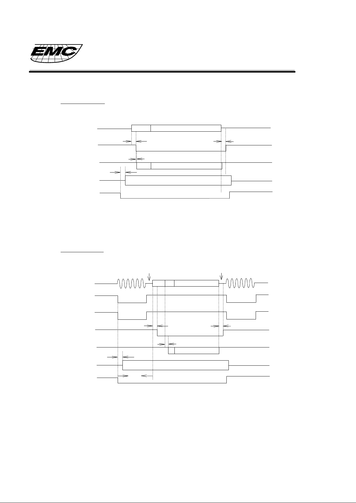
Off-hook FSK :
2. SHORTDATA timing
On-hook FSK :
ps. Typically, on-hook FSK signal has to be at least TCDL =
15ms of Channel Seizure time and TSDV = 12.5ms of
Mark bits time for SHORTDATA timing detected valid.
TIP/RING
/CD
DATA OUT
OSC
DATA
T
CDL
/PWUP
3.58MHz
T
DOC
T
CDH
T
OSC
1
M FSK data
TIP/RING
/CD
SHORTDATA
OSC
FIRST RING
2 SECONDS
0.5 SEC
0.5 SEC
SECOND RING
2 SECONDS
DATA
T
CDL
/PWUP
3.58MHz
T
SDV
T
CDH
T
OSC
1
/RING TIME
/RD
T
SUP
CS M
FSK data
Page 10
EM92547A/B/D
CALLER ID FSK DECODER
________________________________________________________________________________________________________________________________________________________
* This specification are subject to be changed without notice. 1998
~ 9 ~
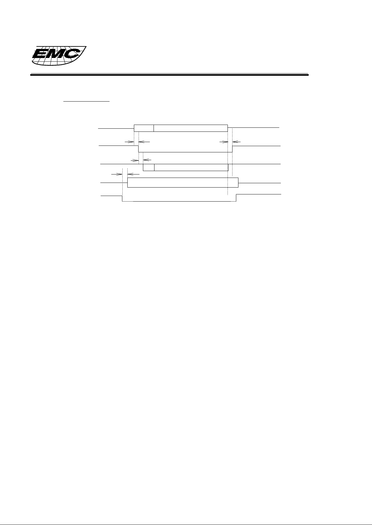
Off-hook FSK :
ps. Typically, off-hook FSK signal has to be at least ‘TCDL +
TSDV = 15ms + 12.5ms = 17.5 ms’ of Mark bits time for
SHORTDATA timing detected valid.
TIP/RING
/CD
SHORTDATA
OSC
DATA
T
CDL
/PWUP
3.58MHz
T
SDV
T
CDH
T
OSC
1
M FSK data
Page 11
EM92547A/B/D
CALLER ID FSK DECODER
________________________________________________________________________________________________________________________________________________________
* This specification are subject to be changed without notice. 1998
~ 10 ~
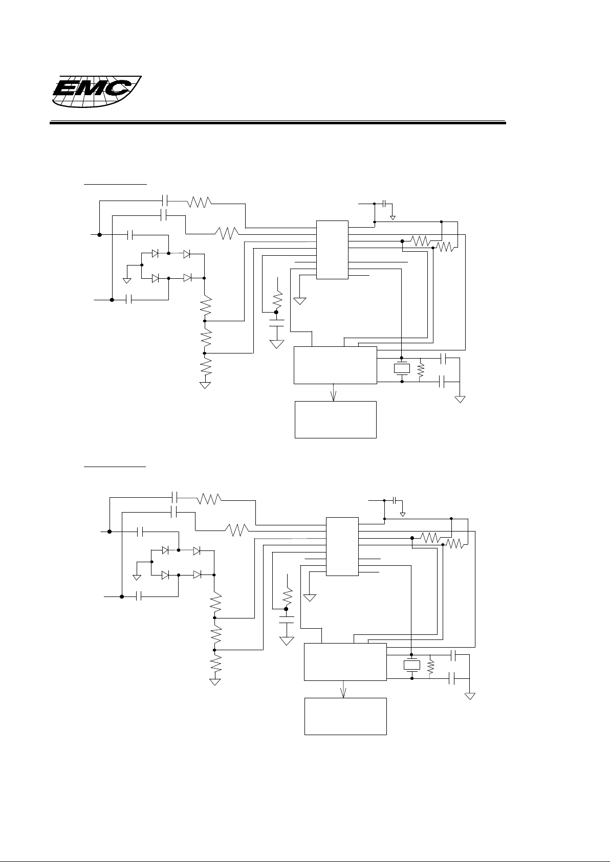
Application Circuit
EM92547A :
EM92547B :
Tip
Ring
Ring det1
Ring det2
/Ring time
/PWR UP
Vdd
DATA OUT
/CD
/RD
NC
OSCIN
Vdd
0.1uF
LCD
DISPLAY
8-bit MCU
15k
18k
470k
0.1u
0.1u
4700p
30k
30k
Vdd
270k
0.22u
47k
47k
33p
33p
3.58M
TIP
RING
1
2
3
4
6
7
8
10
11
12
13
14
16
EM92547B
250V
250V
1M
4700p
NC
5
9
OSCOUT
VSS
Tip
Ring
Ring det1
Ring det2
/Ring time
/PWR UP
Vdd
DATA OUT
/CD
/RD
CLK SELECT
OSCIN
Vdd
0.1uF
LCD
DISPLAY
8-bit MCU
15k
18k
470k
0.1u
0.1u
4700p
30k
30k
Vdd
270k
0.22u
47k
47k
33p
33p
3.58M
TIP
RING
Vdd
1
2
3
4
6
7
8
10
11
12
13
14
16
EM92547A
250V
250V
1M
4700p
NC
5
9
OSCOUT
VSS
Page 12
EM92547A/B/D
CALLER ID FSK DECODER
________________________________________________________________________________________________________________________________________________________
* This specification are subject to be changed without notice. 1998
~ 11 ~
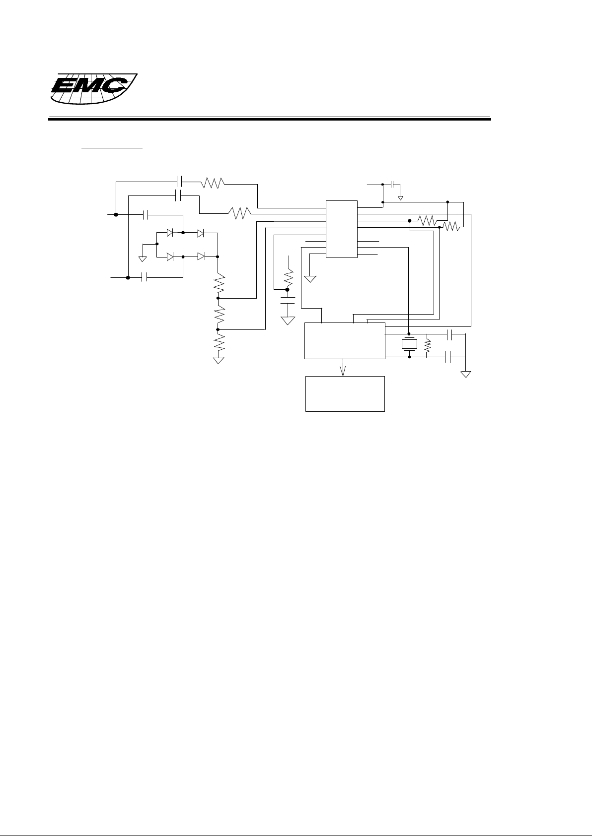
EM92547D :
Tip
Ring
Ring det1
Ring det2
/Ring time
/PWR UP
Vdd
SHORTDATA
/CD
/RD
NC
OSCIN
Vdd
0.1uF
LCD
DISPLAY
8-bit MCU
15k
18k
470k
0.1u
0.1u
4700p
30k
30k
Vdd
270k
0.22u
47k
47k
33p
33p
3.58M
TIP
RING
1
2
3
4
6
7
8
10
11
12
13
15
16
EM92547D
250V
250V
1M
4700p
NC
5
9
OSCOUT
VSS
Page 13
EM92547A/B/D
CALLER ID FSK DECODER
________________________________________________________________________________________________________________________________________________________
* This specification are subject to be changed without notice. 1998
~ 12 ~
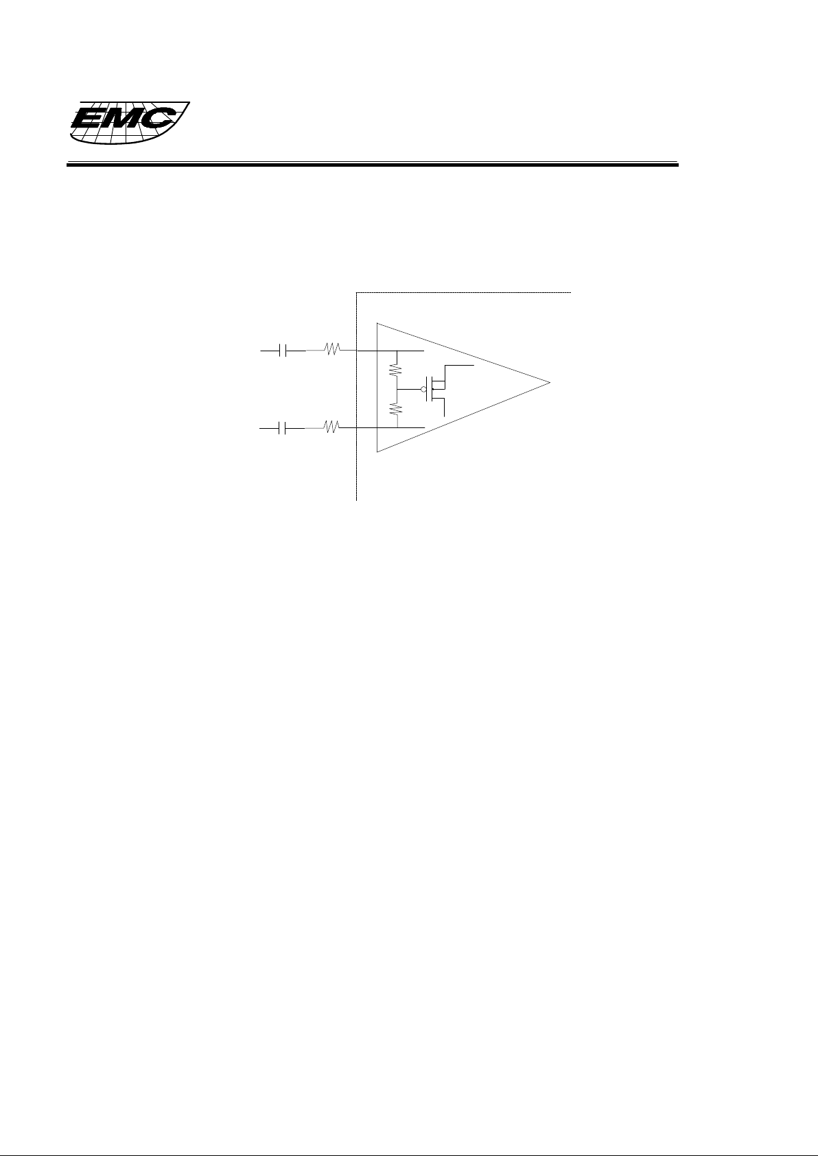
Application Note
1. Input capacitor and input resistor
Input voltage of OP Amp are "A" and "B" which are equal to 500k/(Z1+500k) and 500k/(Z2+500k),
where Z1=Zc1+R1, Z2=Zc2+R2. There is no difference in the input sensitivity when the external
resistors R1 and R2 is more less than 500k ohms. Although R1 and R2 will not critically effect input
sensitivity, we suggest the value of R1 and R2 are 30k to 50k to reduce the ring current into "A" and
"B" for stable operation.
Input coupling capacitors C1 and C2 will slightly effect the input sensitivity. The value of C1 and
C2 could not choose too large to avoid ring voltage discharge time debiasing OP Amp. We suggest
that the value C1 and C2 are less than 0.01uF.
2. VDD pin and VSS pin
To reduce noise effects, connect a ceramic capacitor of about 0.1uF set as close as possible to the
pin to the VSS pin.
3. OSCIN pin, OSCOUT pin
For proper oscillator working, the feedback resistor 1MΩ should be shunt with the 3.58MHz crystal
and 20pF capacitors connected from these two pins to the ground.
500k
500k
C1
C2
R1
R2
A
B
TIP
RING
Differential Input
OP Amp
 Loading...