

Page 1
EL7571C
Programmable PWM Controller
EL7571C
Features
• Pentium® II Compatible
• 5 bit DAC Controlled Output Voltage
• Greater than 90% Efficiency
• 4.5V to 12.6V Input Range
• Dual NMOS Power FET Drivers
• Fixed frequency, Current Mode
Control
• Adjustable Oscillator with External
Sync. Capability
• Synchronous Switching
• Internal Soft-Start
• User Adjustable Slope
Compensation
• Pulse by Pulse Current Limiting
• 1% Typical Output Accuracy
• Power Good Signal
• Output Power Down
• Over Voltage Protection
Applications
• Pentium® II Voltage Regulation
Modules (VRMs)
• PC Motherboards
• DC/DC Converters
• GTL Bus Termination
• Secondary Regulation
Ordering Information
Part No Temp. Range Package Outline #
EL7571C 0°C to +70°C 20-Pin SO MDP0027
General Description
The EL7571C is a flexible, high efficiency, current mode, PWM step
down controller. It incorporates five bit DAC adjustable output voltage
control which conforms to the Intel Voltage Regulation Module (VRM)
Specification for Pentium® II and Pentium® Pro class processors. The
controller employs synchronous rectification to deliver efficiencies
greater than 90% over a wide range of supply voltages and load conditions. The on-board oscillator frequency is externally adjustable, or may
be slaved to a system clock, allowing optimization of RFI performance in
critical applications. In single supply operation, the high side FET driver
supports boot-strapped operation. For maximum flexibility, system operation is possible from either a 5V rail, a single 12V rail, or dual supply
rails with the controller operating from 12V and the power FETs from
5V.
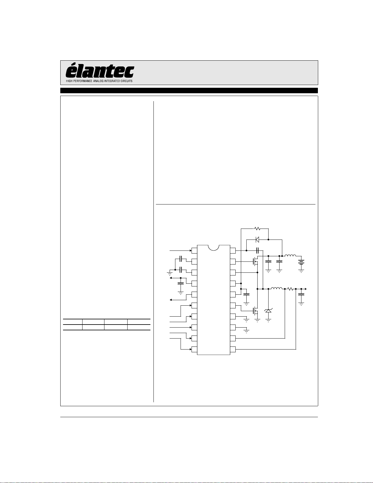
Connection Diagram
R2
5Ω
D1
ENABLE
1.4V
POWER
GOOD
Voltage
(VID
(0:4))
1
2
3
4
5
6
7
8
9
OTEN
CSLOPE
COSC
REF
PWRGD
VIDO
VID1
VID2
VID3
C3 240pF
C3 240pF
C3
0.1µF
I.D.
VH1
HSD
VIN
VINP
LSD
GNDP
GND
20
19
18
LX
17
16
15
14
13
12
CS
C6 0.1µF
Q1
C7
1µF
Q2 D2
1.5µH
C8
1µFC11000µF
x3
L1
5.1µH
L2
4.5V
to
12.6V
V
OUT
1.3V to
3.5V
R2
C2
5Ω
1000µF
x6
10
VID4
Q1, Q2: Siliconix, Si4410, x2
C1: Sanyo, 16MV 1000GX, 1000µF x3
C2: Sanyo, 6MV 1000GX, 1000µF x6
L1: Pulse Engineering, PE-53700, 5.1µH
L2: Micrometals, T30-26, 7T AWG #20, 1.5µH
R1: Dale, WSL-25-12, 15mΩ, x2
D1: BAV99
D2: IR, 32CTQ030
Note: All information contained in this data sheet has been carefully checked and is believed to be accurate as of the date of publication; however, this data sheet cannot be a “controlled document”. Current revisions, if any, to these
specifications are maintained at the factory and are available upon your request. We recommend checking the revision level before finalization of your design documentation.
© 2001 Elantec Semiconductor, Inc.
11
FB
April 24, 2001
Page 2
EL7571C
Programmable PWM Controller
EL7571C
Absolute Maximum Ratings (T
Supply Voltage: -0.5V to 14V
Input Pin Voltage: -.03 below Ground, +0.3 above Supply
VHI -0.5V to 27V
Storage Temperature Range: 65°C to +150°C
= 25°C)
A
Operating Temperature Range: 0°C to +70°C
Operating Junction Temperature: 125°C
Peak Output Current: 3A
Power Dissipation: SO20 500mW
Important Note:
All parameters having Min/Max specifications are guaranteed. Typ values are for information purposes only. Unless otherwise noted, all tests are at the
specified temperature and are pulsed tests, therefore: TJ = TC = TA.
DC Electrical Characteristics
TA = 25°C, VIN = 5V, C
Parameter Description Condition Min Typ Max Unit
V
IN
V
UVLO HI
V
UVLO LO
V
OUT RANGE
V
OUT 1
V
OUT 2
V
REF
V
ILIM
V
IREV
V
OUT PG
V
OVP
V
OTEN LO
V
OTEN HI
V
ID LO
V
ID HI
V
OSC
V
PWRGD LO
R
DS ON
R
FB
R
CS
I
VIN
I
VIN DIS
I
SOURCE/SINK
I
RAMP
I
OSC CHARGE
I
OSC
DISCHARGE
I
REFMAX
I
VID
I
OTEN
= 330pF, C
OSC
SLOPE
= 390pF, R
= 7.5mΩ unless otherwise specified.
SENSE
Input Voltage Range 4.5 12.6 V
Input Under Voltage Lock out Upper Limit Positive going input voltage 3.6 4 4.4 V
Input Under Voltage Lock out Lower Limit Negative going input voltage 3.15 3.5 3.85 V
Output Voltage Range See VID table 1.3 3.5 V
Steady State Output Voltage Accuracy, VID =
10111
Steady State Output Voltage Accuracy, VID =
00101
IL = 6.5A, V
IL = 6.5A, V
= 2.8V 2.74 2.82 2.90 V
OUT
=1.8V 1.74 1.81 1.9 V
OUT
Reference Voltage 1.396 1.41 1.424 V
Current Limit Voltage V
Current Reversal Threshold V
Output Voltage Power Good Lower Level V
= (VCS-VFB) 125 154 185 mV
ILIM
= (VCS-VFB) -40 -5 20 mV
IREV
= 2.05V -18 -14 -10 %
OUT
Output Voltage Power Good Upper Level 8 12 16 %
Over-Voltage Protection Threshold +9 +13 +17 %
Power Down Input Low Level VIN = -10uA 1.5 V
Power Down Input High Level (VIN-1.5) V
Voltage I.D. Input Low Level 1.5 V
Voltage I.D. Input High Level (VIN-1.5) V
Oscillator Voltage Swing 0.85 V
Power Good Output Low Level I
HSD, LSD Switch On-Resistance VIN, V
= 1mA 0.5 V
OUT
INP
LX) = 12V
= 12V, I
= 100mA, (VHI-
OUT
4.8 6 Ω
FB Input Impedance 9.5 kΩ
CS Input Impedance 115 kΩ
Quiescent Supply Current V
Supply Current in Output Disable Mode V
Peak Driver Output Current VIN,V
C
Ramp Current High Side Switch Active 8.5 14 20 µA
SLOPE
Oscillator Charge Current 1.2>V
Oscillator Discharge Current 1.2>V
>(VIN-0.5)V 1.2 2 mA
OTEN
<1.5V 0.76 1 mA
OTEN
= 12V, Measured at HSD, LSD,
INP
(VHI-LX) = 12V
>0.35V 50 µA
OSC
>0.35V 2 mA
OSC
2.5 A
VREF Output Current 25 µA
VID Input Pull up Current 3 5 7 µA
OTEN Input Pull up Current 3 5 7 µA
P-P
2
Page 3
EL7571C
Programmable PWM Controller
AC Electrical Characteristics
TA = 25°C, VIN = 5V, C
Parameter Description Conditions Min Typ Max Unit
f
OSC
f
CLK
t
OTEN
t
SYNC
T
START
D
MAX
Pin Descriptions
Pin No.
1. Pin designators: I = Input, O = Output, S = Supply
Pin
Name
1 OTEN I Chip enable input, internal pull up (5mA typical). Active high.
2 CSLOPE I With a capacitor attached from CSLOPE to GND, generates the voltage ramp compensation for the PWM current mode con-
3 COSC I Multi-function pin: with a timing capacitor attached, sets the internal oscillator rate fS (kHz) = 57/C
4 REF O Band gap reference output. Decouple to GND with 0.1uF.
5 PWRGD O Power good, open drain output. Set low whenever the output voltage is not within ±13% of the programmed value.
6 VID0 I Bit 0 of the output voltage select DAC. Internal pull up sets input high when not driven.
7 VID1 I Bit 1 of the output voltage select DAC. Internal pull up sets input high when not driven.
8 VID2 I Bit 2 of the output voltage select DAC. Internal pull up sets input high when not driven.
9 VID3 I Bit 3 of the output voltage select DAC. Internal pull up sets input high when not driven.
10 VID4 I Bit 4 of the output voltage select DAC. Internal pull up sets input high when not driven.
11 FB I Voltage regulation feedback input. Tie to V
12 CS I Current sense. Current feedback input of PWM controller and over current capacitor input. Current limit threshold set at
13 GND S Ground
14 GNDP S Power ground for low side FET driver. Tie to GND for normal operation.
15 LSD O Low side gate drive output.
16 VINP S Input supply voltage for low side FET driver. Tie to VIN for normal operation.
17 VIN S Input supply voltage for control unit.
18 LX S Negative supply input for high side FET driver.
19 HSD O High side gate drive output. Driver ground referenced to LX. Driver supply may be bootstrapped to enhance low controller
20 VH1 S Positive supply input for high side FET driver.
= 330pF, C
OSC
Nominal Oscillator Frequency C
Clock Frequency 50 500 1000 kHz
Shutdown Delay V
Oscillator Sync. Pulse Width Oscillator i/p (COSC) driven with HCMOS
Soft-start Period V
Maximum Duty Cycle 97 %
Pin
[1]
Type
= 390pF unless otherwise specified.
SLOPE
= 330pF 140 190 240 kHz
OSC
>1.5V 100 ns
OTEN
gate
= 3.5V 100/f
OUT
Function
troller. Slope rate is determined by an internal 14uA pull up and the C
the termination of the high side cycle.
low for a duration t
+154mV with respect to FB. Connect sense resistor between CS and FB for normal operation.
input voltage operation.
synchronizes device to an external clock.
SYNC
for normal operation.
OUT
20 800 ns
capacitor value. VC
SLOPE
CLK
SLOPE
OSC
is reset to ground at
(µF); when pulsed
EL7571C
us
3
Page 4
EL7571C
Programmable PWM Controller
EL7571C
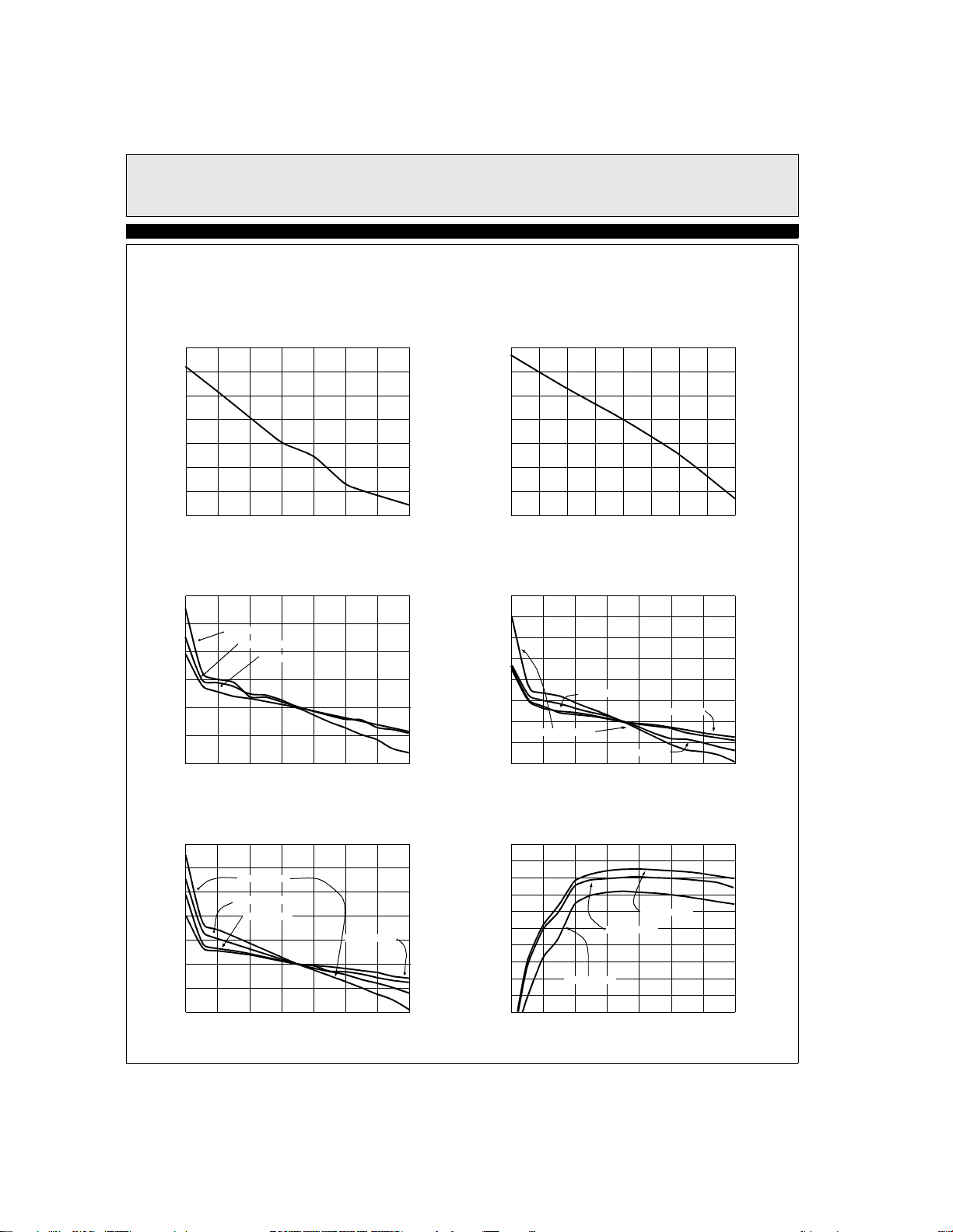
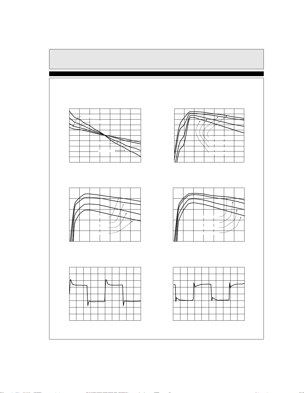
Typical Performance Curves
+12V Supply Sync Line Regulation
0.004
0.003
0.002
0.001
0
Line Regulation (%)
-0.001
-0.002
-0.003
13.5 10.011.5 11.0 10.513.0 12.5 12.0
+12V Supply Sync Load Regulation
0.04
0.03
0.02
0.01
0
Load Regulation (%)
-0.01
-0.02
V
= 1.8V
OUT
V
= 2.1V
OUT
V
0 1 3 5 11 1397
OUT
VIN (V)
= 2.8V
I
OUT
5V Supply Line Regulation
0.30
0.20
0.10
0.00
-0.10
Line Regulation (%)
-0.20
-0.30
-0.40
5.50 4.505.005.25 4.75
VRM +5V Supply +12V Controller Sync w/o
Schottky Load Regulation
6.00
5.00
4.00
3.00
2.00
1.00
Load Regulation (%)
0
V
-1.00
-2.00
(A)
OUT
0 1 3 5 11 1397
= 1.3V
VIN (V)
V
= 2.8V
OUT
V
= 3.5V
OUT
V
= 1.8V
OUT
I
(A)
OUT
+5V Supply Non-Sync Load Regulation
5.00
4.00
3.00
2.00
1.00
Load Regulation (%)
0
-1.00
-2.00
0 1 3 5 11 1397
V
= 1.3V
OUT
V
= 1.8V
OUT
V
= 2.8V
OUT
+12V Supply Sync Efficiency
1.0
0.9
0.8
V
= 3.5V
OUT
I
(A)
OUT
0.7
Efficiency (%)
0.6
0.5
0 1 3 5 11 1397
V
= 1.8V
OUT
V
= 3.5V
OUT
V
= 2.8V
OUT
I
(A)
OUT
4
Page 5
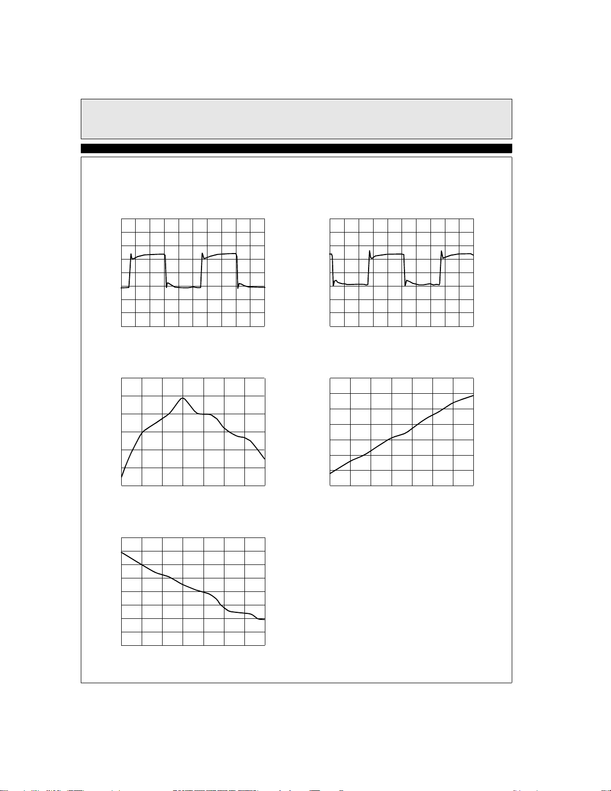
Typical Performance Curves
EL7571C
EL7571C
Programmable PWM Controller
+5V Supply Sync with Schottky Load
2.5
V
= 3.5V
1.5
0.5
0
-0.5
Load Regulation (%)
-1.5
-2.5
0
1.0
0.9
0.8
0.7
Efficiency (%)
0.6
0.5
0 1 3 5 11 1397 0 1 3 5 11 1397
OUT
V
= 2.8V
OUT
V
= 1.8V
OUT
V
= 1.3V
OUT
1 3 5 11 1397
I
(A)
OUT
+5V Supply Non-Sync VRM Efficiency
V
= 3.5V
OUT
V
= 2.8V
OUT
V
= 1.8V
OUT
V
= 1.3V
OUT
I
(A)
OUT
+5V Supply +12V Controller Sync w/o Schottky
VRM Efficiency
1.0
0.9
0.8
0.7
Efficiency (X)
0.6
0.5
0.02
1.02 3.04 5.04 11.04 13.049.047.04
+5V Supply Sync with Schottky VRM Efficiency
1.0
0.9
0.8
0.7
Efficiency (%)
0.6
0.5
V
= 3.5V
OUT
V
= 1.8V
OUT
V
= 2.8V
OUT
V
= 1.3V
OUT
I
(A)
OUT
V
= 3.5V
OUT
V
= 2.8V
OUT
V
= 1.8V
OUT
V
= 1.3V
OUT
I
(A)
OUT
12V Transient Response
1
5V Non-sync Transient Response
1
5
Page 6
EL7571C
Programmable PWM Controller
EL7571C
Typical Performance Curves
5V Sync Transient Response
1
Efficiency vs Temperature
92.6
92.5
92.4
92.2
Efficiency (%)
92.0
91.8
91.6
-45 6015 30 45-30 -15 0
Temperature (°C)
5V Input 12V Controller Transient Response
1
V
vs Temperature
REF
1.425
1.420
1.415
1.410
(V)
REF
1.405
V
1.400
1.395
1.390
-45 6015 30 45-30 -15 0
Temperature (°C)
Frequency vs Temperature
280
270
260
250
240
230
Frequency (KHz)
220
210
200
-45 6015 30 45-30 -15 0
Temperature (°C)
6
Page 7

Applications Information
Circuit Description
EL7571C
EL7571C
Programmable PWM Controller
General
The EL7571C is a fixed frequency, current mode, pulse
width modulated (PWM) controller with an integrated
high precision reference and a 5 bit Digital-to-Analog
Converter (DAC). The device incorporates all the active
circuitry required to implement a synchronous step
down (buck) converter which conforms to the Intel Pentium® II VRM specification. Complementary switching
outputs are provided to drive dual NMOS power FET’s
in either synchronous or non-synchronous configurations, enabling the user to realize a variety of high
efficiency and low cost converters.
Reference
A precision, temperature compensated band gap reference forms the basis of the EL7571C. The reference is
trimmed during manufacturing and provides 1% set
point accuracy for the overall regulator. AC rejection of
the reference is optimized using an external bypass
capacitor C
REF
.
Main Loop
A current mode PWM control loop is implemented in
the EL7571C (see block diagram). This configuration
employs dual feedback loops which provide both output
voltage and current feedback to the controller. The
resulting system offers several advantages over tradititional voltage control systems, including simpler loop
design, pulse by pulse current limiting, rapid response to
line variaion and good load step response. Current feedback is performed by sensing voltage across an external
shunt resistor. Selection of the shunt resistance value
sets the level of current feedback and thereby the load
regulation and current limit levels. Consequently, operation over a wide range of output currents is possible. The
reference output is fed to a 5 bit DAC with step weighing conforming to the Intel VRM Specification. Each
DAC input includes an internal current pull up which
directly interfaces to the VID output of a Pentium® II
class microprocessor. The heart of the controller is a triple-input direct summing differential comparator, which
sums voltage feedback, current feedback and compen-
sating ramp signals together. The relative gains of the
comparator input stages are weighed. The ratio of voltage feedback to current feedback to compensating ramp
defines the load regulation and open loop voltage gain
for the system, respectively. The compensating ramp is
required to maintain large system signal system stability
for PWM duty cycles greater than 50%. Compensation
ramp amplitude is user adjustable and is set with a single
external capacitor (CSLOPE). The ramp voltage is
ground referenced and is reset to ground whenever the
high side drive signal is low. In operation, the DAC output voltage is compared to the regulator output, which
has been internally attenuated. The resulting error voltage is compared with the compensating ramp and
current feedback voltage. PWM duty cycle is adjusted
by the comparator output such that the combined comparator input sums to zero. A weighted comparator
scheme enhances system operation over traditional voltage error amplifier loops by providing cycle-by-cycle
adjustment of the PWM output voltage, eliminating the
need for error amplifier compensation. The dominant
pole in the loop is defined by the output capacitance and
equivalent load resistance, the effect of the output inductor having been canceled due to the current feedback. An
output enable (OUTEN) input allows the regulator output to be disabled by an external logic control signal.
Auxiliary Comparators
The current feedback signal is monitored by two additional comparators which set the operating limits for the
main inductor current. An over current comparator terminates the PWM cycle independently of the main
summing comparator output whenever the voltage
across the sense resistor exceeds 154mV. For a 7.5mΩ
resistor this corresponds to a nominal 20A current limit.
Since output current is continuously monitored, cycleby-cycle current limiting results. A second comparator
senses inductor current reverse flow. The low side drive
signal is terminated when the sense resistor voltage is
less than -5mV, corresponding to a nominal reverse cur-
rent of -0.67A, for a 7.5mΩ sense resistor. Additionally,
under fault conditions, with the regulator output over-
7
Page 8

EL7571C
Programmable PWM Controller
EL7571C
voltage, inductor current is prevented from ramping to a
high level in the reverse direction. This prevents the parasitic boost action of the local power supply when the
fault is removed and potential damage to circuitry connected to the local supply.
Oscillator
A system clock is generated by an internal relaxation
oscillator. Operating frequency is simple to adjust using
a single external capacitor C
discharge current in the oscillator is well defined and
sets the maximum duty cycle for the system at around
96%.
. The ratio of charge to
OSC
Soft-start
During start-up, potentially large currents can flow into
the regulator output capacitors due to the fast rate of
change of output voltage caused during start-up,
although peak inrush current will be limited by the over
current comparator. However an additionally internal
switch capacitor soft-start circuit controls the rate of
change of output voltage during start-up by overriding
the voltage feedback input of the main summing comparator, limiting the start-up ramp to around 1ms under
typical operating conditions. The soft-start ramp is reset
whenever the output enable (OUTEN) is reset or whenever the controller supply falls below 3.5V.
Watchdog
A system watchdog monitors the condition of the controller supply and the integrity of the generated output
voltage. Modern logic level power FET’s rapidly
increase in resistivity (Rdson) as their gate drive is
reduced below 5V. To prevent thermal damage to the
power FET’s under load, with a reduced supply voltage,
the system watchdog monitors the controller supply
(VIN) and disables both PWM outputs (HSD, LSD)
when the supply voltage drops below 3.5V. When the
supply voltage is increased above 4V the watchdog initiates a soft-start ramp and enables PWM operation. The
difference between enable and disable thresholds introduces hysteresis into the circuit operation, preventing
start-up oscillation. In addition, output voltage is also
monitored by the watchdog. As called out by the Intel
Pentium® II VRM specification, the watchdog power
good output (PWRGD) is set low whenever the output
voltage differs from it’s selected value by more than
±13%. PWRGD is an open drain output. A third watchdog function disables PWM output switching during
over-voltage fault conditions, displaying both external
FET drives, whenever the output voltage is greater than
13% of its selected value, thereby anticipating reverse
inductor current ramping and conforming to the VRM
over-voltage specification, which requires the regulator
output to be disabled during fault conditions. Switching
is enabled after the fault condition is removed.
Output Drivers
Complementary control signals developed by the PWM
control loop are fed to dual NMOS power FET drivers
via a level shift circuit. Each driver is capable of delivering nominal peak output currents of 2A at 12V. To
prevent shoot-through in the external FET’s, each driver
is disabled until the gate voltage of the complementary
power FET has fallen to less than 1V. Supply connections for both drivers are independent, allowing the
controller to be configured with a boot-strapped high
side drive. Employing this technique a single supply
voltage may be used for both power FET’s and controller. Alternatively, the application may be simplified
using dual supply rails with the power FET’s connected
to a secondary supply voltage below the controller’s,
typically 12V and 5V. For applications where efficiency
is less important than cost, applications can be further
simplified by replacing the low side power FET with a
Schottky diode, resulting in non-synchronous operation.
Applications Information
The EL7571C is designed to meet the Intel 5 bit VRM
specification. Refer to the VID decode table for the controller output voltage range.
The EL7571C may be used in a number converter topologies. The trade-off between efficiency, cost, circuit
complexity, line input noise, transient response and
availability of input supply voltages will determine
which converter topology is suitable for a given applica-
8
Page 9

EL7571C
Programmable PWM Controller
tion. The following table lists some of the differences
between the various configurations:
Converter Topologies
Topology Diagram Efficiency Cost Complexity Input Noise
5V only Non-synchronous figure 1 92% low low high good
5V only Synchronous figure 2 95% higher higher high good
5V &12V Non-synchronous figure 3 92% lowest lowest high good
5V & 12V Synchronous figure 4 95% high high high good
12V only Synchronous Connection
Diagram
92% highest highest high best
Transient
Response
EL7571C
Circuit schematics and Bills of Material (BOMs) for the
various topologies are provided at the end of this data
sheet. If your application requirements differ from the
included samples, the following design guide lines
should be used to select the key component values.
Refer to the front page connection diagram for component locations.
Output Inductor, L
1
Two key converter requirements are used to determine
inductor value:
• I
- minimum output current; the current level at
MIN
which the converter enters the discontinuous mode of
operation (refer to Elantec application note #18 for a
detailed discussion of discontinuous mode)
• I
- maximum output current
MAX
Although many factors influence the choice of the
inductor value, including efficiency, transient response
and ripple current, one practical way of sizing the inductor is to select a value which maintains continuous mode
operation, i.e. inductor current positive for all conditions. This is desirable to optimize load regulation and
light load transient response. When the minimum inductor ripple current just reaches zero and with the mean
ripple current set to I
twice I
, independent of duty cycle. The minimum
MAX
, peak inductor ripple current is
MIN
inductor value is given by:
L
1MIN
V(
-----------------------------------------------------
INVOUT
1
PEAK
) TON×–
V(
---------------------------------------------------------==
VINFSW2 I
INVOUT
) V
×–
OUT
×××
MIN
where:
I
= peak ripple current
PEAK
T
= top switch on time
ON
VIN = input voltage
FSW = switching frequency
V
= output voltage
OUT
I
= minimum load
MIN
Since inductance value tends to decrease with current,
ripple current will generally be greater than 21
MIN
higher output current.
Once the minimum output inductance is determined, an
off the shelf inductor with current rating greater than the
maximum DC output required can be selected. Pulse
Engineering and Coil Craft are two manufactures of
high current inductors. For converter designers who
want to design their own high current inductors, for
experimental purposes or to further reduce costs, we recommend the Micrometals Powered Iron Cores data
sheet and applications note as a good reference and starting point.
Current Sense Resistor, R
1
Inductor current is monitored indirectly via a low value
resistor R1. The voltage developed across the current
sense resistor is used to set the maximum operating current, the current reversal threshold and the system load
regulation. To ensure reliable system operation it is
important to sense the actual voltage drop across the
resistor. Accordingly a four wire Kelvin connection
should be made to the controller current sense inputs.
at
9
Page 10

EL7571C
Programmable PWM Controller
EL7571C
There are two criteria for selecting the resistor value and
type. Firstly, the minimum value is limited by the maximum output current. The EL7571C current limit
capacitor has a typical threshold of 154mV, 125mV
minimum. When the voltage across the sense resistor
exceeds this threshold, the conduction cycle of the top
switch terminates immediately, providing pulse by pulse
current limiting. A resistor value must be selected which
guarantees operation under maximum load. That is:
V
OCMIN
R
---------------------=
1
1
MAX
where:
V
I
= minimum over current voltage threshold
OCMIN
= maximum output current
MAX
Secondly, since the load current passes directly through
the sense resistor, its power rating must be sufficient to
handle the power dissipated during maximum load (current limit) conditions. Thus:
OUTMAX
2
R
×=
1
PD1
where:
PD = power dissipated in current sense resistor
PD must be less than the power rating of the current
sense resistor. High current applications may require
parallel sense resistors to dissipate sufficient power.
Current Sense Resistor Table below lists some popular
current sense resistors: the WLS-2512 series of Power
Metal Strip Resistors from Dale Electronics, OARS
series Iron Alloy resistor from IRC, and Copper Magnanin (CuNi) wire resistor from Mills Resistors. Mother
board copper trace is not recommended because of its
high temperature coefficient and low power dissipation.
The trade-off between the different types of resistors are
cost, space, packaging and performance. Although
Power Metal Strip Resistors are relatively expensive,
they are available in surface mount packaging with
tighter tolerances. Consequently, less board space is
used to achieve a more accurate current sense. Alternatively, Magnanin copper wire has looser tolerance and
higher parasitic inductance. This results in a less current
sense but at a much lower cost. Metal track on the PCB
can also be used as current sense resistor. The trade-offs
are ±30% tolerance and ±4000 ppm temperature coefficient. Ultimately, the selection of the type of current
sense element must be made on an application by application basis.
Bill of Materials
Manufacturer Part No. Tolerance
Dale WSL 2512 ±1% ±75ppm 1 W 402-563-6506 402-563-6418
IRC OARS Series ±5% ±20ppm 1W - 5W 800-472-6467 800-472-3282
Mills Resistor MRS1367-TBA ±10% ±20ppm 1.2W 916-422-5461 906-422-1409
PCB Trace Resistor ±30% ±4000ppm 50A/in (1oz Cu)
Input Capacitor, C
1
In a buck converter, where the output current is greater
than 10A, significant demand is placed on the input
capacitor. Under steady state operation, the high side
FET conducts only when it is switched “on” and conducts zero current when it is turned “off”. The result is a
current square wave drawn from the input supply. Most
of this input ripple current is supplied from the input
capacitor C1. The current flow through C1’s equivalent
series resistance (ESR) can heat up the capacitor and
Temperature
Coefficient Power Rating Phone No. Fax No.
cause premature failure. Maximum input ripple current
occurs when the duty cycle is 50%, a current of Iout/2
RMS.
Worst case power dissipation is:
P
D
•=
-------------
2
ESR
IN
2
I
OUT
where:
ERSIN = input capacitor ESR
10
Page 11

EL7571C
Programmable PWM Controller
EL7571C
For safe and reliable operation, PD must be less than the
capacitor’s data sheet rating.
Input Inductor, L
2
The input inductor (L2) isolates switching noise from
the input supply line by diverting buck converter input
ripple current into the input capacitor. Buck regulators
generate high levels of input ripple current because the
load is connected directly to the supply through the top
switch every cycle, chopping the input current between
the load current and zero, in proportion to the duty cycle.
The input inductor is critical in high current applications
where the ripple current is similarly high. An exclusively large input inductor degrades the converter’s load
transient response by limiting the maximum rate of
change of current at the converter input. A 1.5µH input
inductor is sufficient in most applications.
Output Capacitor, C
2
During steady state operation, output ripple current is
much less than the input ripple current since current flow
is continuous, either via the top switch or the bottom
switch. Consequently, output capacitor power dissipation is less of a concern than the input capacitor’s.
However, low ESR is still required for applications with
very low output ripple voltage or transient response
requirements. Output ripple voltage is given by:
V
RIPIRIP
ESR
×=
OUT
where:
I
= output ripple current
RIP
ESR
= output capacitor ESR
OUT
During a transient response, the output voltage spike is
determined by the ESR and the equivalent series inductance (ESL) of the output capacitor in addition to the rate
of change and magnitude of the load current step. The
output voltage transient is given by:
∆V
ESR
=
OUT
OUT∆IOUT
ESL
d
i
×+×
----
d
t
where:
ESR
= output capacitor ESR
OUT
ESL = output capacitor ESL
∆I
= output current step
OUT
di/dt = rate of change of output current
Power MOSFET, Q1 and Q2
The EL7571C incorporates a boot-strap gate drive
scheme to allow the usage of N-channel MOSFETs. Nchannel MOSFETs are preferred because of their relative low cost and low on resistance. The largest amount
of the power loss occurs in the power MOSFETs, thus
low on resistance should be the primary characteristic
when selecting power MOSFETs. In the boot-strap gate
drive scheme, the gate drive voltage can only go as high
as the supply voltage, therefore in a 5V system, the
MOSFETs must be logic level type, Vgs<4.5V. In addition to on resistance and gate to source threshold, the
gate to source capacitance is also very important. In the
region when the output current is low (below5A),
switching loss is the dominant factor. Switching loss is
determined by:
2
PCV
where:
C is the gate to source capacitance of the MOSFET
V is the supply voltage
F is the switching frequency
Another undesirable reason for a large MOSFET gate to
source capacitance is that the on resistance of the MOSFET driver can not supply the peak current required to
turn the MOSFET on and off fast. This results in additional MOSFET conduction loss. As frequency
increases, this loss also increases which leads to more
power loss and lower efficiency.
Finally, the MOSFET must be able to conduct the maximum current and handle the power dissipation.
The EL7571C is designed to boot-strap to 12V for 12V
only input converters. In this application, logic level
MOSFETs are not required.
Table below lists a few popular MOSFETs and their critical specifications.
F××=
11
Page 12

EL7571C
Programmable PWM Controller
EL7571C
Manufacturer Model Vgs Ron (max) Cgs ID VDS Package
MegaMos Mi4410 4.5V 20mΩ 6.4nF ±10A 30V SO-8
MegaMos Mip30N03A 4.5V 22mΩ 6.3nF ±15A 30V TO-220
Siliconix Si4410 4.5V 20mΩ 4.3nF ±10A 30V SO-8
Fuji 2SK1388 4V 37mΩ ±17.5A TO-220
IR IRF3205S 4 8mΩ 17nF (max) ±98A 55V D2Pak
Motorola MTB75N05HD 4 7mΩ 7.1nF ±75A 50V TO-220
Skottky Diode, D2
In the non-synchronous scheme a flyback diode is
required to provide a current path to the output when the
high side power MOSFET, Q1, is switched off. The critical criteria for selecting D2 is that it must have low
forward voltage drop. The product of forward voltage
drop and condition current is a primary source of power
dissipation in the convertor. The Schottky diode selected
is the International Rectifier 32CTQ030 which has 0.4V
of forward voltage drop at 15A.
12
Page 13

Block Diagram
ENABLE
In
Regulation
EL7571C
EL7571C
Programmable PWM Controller
12.6V
Reference
4V
UVLO HI
+
-
UVLO LOW
+
-
3.5V
Oscillator
0.1µF
DAC
Ramp Control
C
S
+
-
+
-
Current Reversal
+
-
+
-
+
∑
-
+
Soft
Start
ENABLE
PWM
Control Logic
INP
V
HI
HSD
0.1µF
LX
5.1µH L
LSD
GNDPGND
V
1
7.5mΩ C
OUT
2
6mF
1.5µH
L
2
3mF4.5V to
VID
(0:4)
240pF
220pF
C
VINOTEN REF FB PWRGD V
1
C
SLOPE
C
OSC
13
Page 14

EL7571C
Programmable PWM Controller
EL7571C
Voltage ID Code Output Voltage Settings
V
ID4
0 1 1 1 1 1.3
0 1 1 1 0 1.35
0 1 1 0 1 1.4
0 1 1 0 0 1.45
0 1 0 1 1 1.5
0 1 0 1 0 1.55
0 1 0 0 1 1.6
0 1 0 0 0 1.65
0 0 1 1 1 1.7
0 0 1 1 0 1.75
0 0 1 0 1 1.8
0 0 1 0 0 1.85
0 0 0 1 1 1.9
0 0 0 1 0 1.95
0 0 0 0 1 2.0
0 0 0 0 0 2.05
1 1 1 1 1 0, No CPU
1 1 1 1 0 2.1
1 1 1 0 1 2.2
1 1 1 0 0 2.3
1 1 0 1 1 2.4
1 1 0 1 0 2.5
1 1 0 0 1 2.6
1 1 0 0 0 2.7
1 0 1 1 1 2.8
1 0 1 1 0 2.9
1 0 1 0 1 3.0
1 0 1 0 0 3.1
1 0 0 1 1 3.2
1 0 0 1 0 3.3
1 0 0 0 1 3.4
1 0 0 0 0 3.5
V
ID3
V
ID2
V
ID1
V
ID0
V
OUT
Application Circuits
To assist the evaluation of EL7571C, several VRM
applications have been developed. These are described
in the converter topologies table earlier in the data sheet.
The demo board can be configured to operate with either
a 5V or 12V controller supply, using a 5V FET supply.
14
Page 15

Programmable PWM Controller
5V Input, Boot-Strapped Non-Synchronous DC:DC Converter
5Ω
D1R2
Q1
C7
0.1µF
0.1µF
D2
C6
C8
1µF
L1 R1
5.1µH
C1
1000µF
x3
1µH
L2
7.5mΩ
ENABLE OTEN
1.4V
0.1µF
POWER
GOOD
1
240pF
2
220pF
3
4
5
6
CSLOPE
COSC
REF
PWRGD
C3
C4
C5
VH1
HSD
V1H
VINP
LSDVIDO
20
19
18
LX
17
16
15
EL7571C
5V
VOUT
C2
1000µ
F
EL7571C
GNDP
GND
14
13
CS
12
FB
11
Voltage
LD.
(VID(0:4))
7
VID1
VID2
8
VID3
9
10
VID4
EL7571C 5V VRM Bill of Materials - 5V Non Sync Solution
Component Manufacturer Part Number Value Unit
C1 Sanyo 6MV1000GX 1000µF 3
C2 Sanyo 6MV1000GX 1000µF 6
C3 Chip Capacitors 240pf 1
C4 Chip Capacitors 220pf 1
C5, C6 Chip Capacitors 0.1µF 2
C7, C8 Chip Capacitors 1µF 2
D1 GI Schotty diode SS12GICT-ND 1
IC1 Elantec EL7571CM 1
L1 Pulse Engineering PE-53700 5.1µH 1
L2 Micrometals T30-26,7T AWG #20 1µH 1
R1 DALE WSL-2512 15mΩ 2
R2 Chip Resistor 5Ω 1
D2 IR IR32CTQ030 1
Q1 Siliconix Si4410 2
15
Page 16

EL7571C
Programmable PWM Controller
EL7571C
5V Input Boot-Strapped Synchronous DC:DC Converter
5Ω
R2
D1
Q1
C7
0.1µF
C6
0.1µF
C8
1µF
D2
Q2
ENABLE OTEN
1.4V
0.1µF
POWER
GOOD
1
240pF
2
220pF
3
4
5
6
7
CSLOPE
COSC
REF
PWRGD
VID1
C3
C4
C5
VH1
HSD
V1H
VINP
LSDVIDO
GNDP
20
19
18
LX
17
16
15
14
C1
1000µF
x3
L1 R1
5.1µH
1.5µH
L2
7.5mΩ
5V
VOUT
C2
1000µ
F
Voltage
LD.
(VID(0:4))
VID2
8
VID3
9
10
VID4
GND
13
CS
12
11
FB
EL7571C 5V VRM Bill of Materials - 5V Non Sync Solution
Component Manufacturer Part Number Value Unit
C1 Sanyo 6MV1000GX 1000µF 3
C2 Sanyo 6MV1000GX 1000µF 6
C3 Chip Capacitors 240pf 1
C4 Chip Capacitors 220pf 1
C5, C6 Chip Capacitors 0.1µF 2
C7, C8 Chip Capacitors 1µF 2
D1 GI Schotty diode SS12GICT-ND 1
IC1 Elantec EL7571CM 1
L1 Pulse Engineering PE-53700 5.1µH 1
L2 Micrometals T30-26,7T AWG #20 1µH 1
R1 DALE WSL-2512 15mΩ 2
R2 Chip Resistor 5Ω 1
D2 IR IR32CTQ030 1
Q1, Q2 Siliconix Si4410 2 each
16
Page 17

5V Input, 12V Controller, Non-Sync Solution
ENABLE OTEN
1.4V
0.1µF
POWER
GOOD
1
220pF
2
220pF
3
4
5
6
7
CSLOPE
COSC
REF
PWRGD
VID1
C3
C4
C5
VH1
HSD
V1H
VINP
LSDVIDO
GNDP
20
19
18
LX
17
16
15
14
Q1
C7
0.1µF
Q2
EL7571C
Programmable PWM Controller
12V
5Ω
R2
1µH
L2
C1
C8
1µF
L1 R1
5.1µH
1000µF
x3
7.5mΩ
5V
VOUT
C2
1000µ
F
EL7571C
Voltage
LD.
(VID(0:4))
VID2
8
VID3
9
10
VID4
GND
13
CS
12
11
FB
EL7571C 5V VRM Bill of Materials - 5V Non Sync Solution
Component Manufacturer Part Number Value Unit
C1 Sanyo 6MV1000GX 1000µF 3
C2 Sanyo 6MV1000GX 1000µF 6
C3 Chip Capacitors 240pF 1
C4 Chip Capacitors 220pF 1
C5 Chip Capacitors 0.1µF 1
C7, C8 Chip Capacitors 1µF 2
IC1 Elantec EL7571CM 1
L1 Pulse Engineering PE-53700 5.1µH 1
L2 Micrometals T30-26,7T AWG #20 1µH 1
R1 DALE WSL-2512 15mΩ 2
R2 Chip Resistor 5Ω 1
D2 IR IR32CTQ030 1
Q1 Siliconix Si4410 2
17
Page 18

EL7571C
Programmable PWM Controller
EL7571C
5V Input, 12V Controller, Synchronous DC:DC Converter
D2
C8
1µF
L1 R1
5.1µH
12V
C1
1000µF
x3
1.5µH
L2
7.5mΩ
5V
VOUT
C2
1000µ
F
ENABLE OTEN
1.4V
0.1µF
POWER
GOOD
Voltage
LD.
(VID(0:4))
1
330pF
2
330pF
3
4
5
6
7
8
9
10
CSLOPE
COSC
REF
PWRGD
VID1
VID2
VID3
VID4
C3
C4
C5
VH1
HSD
V1H
VINP
LSDVIDO
GNDP
GND
C6
20
19
18
LX
17
16
15
14
13
CS
12
11
FB
0.1µF
Q1
C7
0.1µF
EL7571C 5V VRM Bill of Materials - 5V Input, 12V Controller Sync Solution
Component Manufacturer Part Number Value Unit
C1 Sanyo 6MV1000GX 1000µF 3
C2 Sanyo 6MV1000GX 1000µF 6
C3 Chip Capacitors 330pf 1
C4 Chip Capacitors 330pf 1
C5, C6 Chip Capacitors 0.1µF 2
C7, C8 Chip Capacitors 1µF 2
IC1 Elantec EL7571CM 1
L1 Pulse Engineering PE-53700 5.1µH 1
L2 Micrometals T30-26,7T AWG #20 1µH 1
R1 DALE WSL-2512 15mΩ 2
D2 IR IR32CTQ030 1
Q1, Q2 Siliconix Si4410 2 each
18
Page 19

PCB Layout Considerations
EL7571C
EL7571C
Programmable PWM Controller
1. Place the power MOSFET’s as close to the controller as possible. Failure to do so will cause
large amounts of ringing due to the parasitic
inductance of the copper trace. Additionally, the
parasitic capacitance of the trace will weaken the
effective gate drive. High frequency switching
noise may also couple to other control lines.
2. Always place the by-pass capacitors (0.1µF and
1µF) as close to the EL7571C as possible. Long
lead lengths will lessen the effectiveness.
3. Separate the power ground (input capacitor
ground and ground connections of the Schottky
diode and the power MOSFET’s) and signal
grounds (ground pins of the by-pass capacitors
and ground terminals of the EL7571C). This will
isolate the highly noisy switching ground from
the very sensitive signal ground.
4. Connect the power and signal grounds at the output capacitors. Output capacitor ground is the
quietest point in the converter and should be
used as the reference ground.
5. The power MOSFET’s output inductor and
Schottky diode should be grouped together to
contain high switching noise in the smallest area.
6. Current sense traces running from pin 11 and pin
12 to the current sense resistor should run parallel and close to each other and be Kelvin
connected (no high current flow). In high current
applications performance can be improved by
connecting low Pass filter (typical values 4.7Ω,
0.1µF) between the sense resistor and the IC
inputs.
19
Page 20

EL7571C
Programmable PWM Controller
EL7571C
Layout Example
To demonstrate the points discussed above, below
shows two reference layouts - a synchronous 5V only
VRM layout and a synchronous 5V only PC board lay-
out. Both layouts can be modified to any application
circuit configuration shown on this data sheet. Gerber
files of the layouts are available from the factory.
Top Layer Silkscreen
Bottom Layer Silkscreen
20
Page 21

Top Layer Metal
EL7571C
EL7571C
Programmable PWM Controller
Bottom Layer Metal
Top Layer Silkscreen
21
Page 22

EL7571C
Programmable PWM Controller
EL7571C
Top Layer Metal
Bottom Layer Metal
22
Page 23

EL7571C
Programmable PWM Controller
EL7571C
General Disclaimer
Specifications contained in this data sheet are in effect as of the publication date shown. Elantec, Inc. reserves the right to make changes in the circuitry or specifications contained herein at any time without notice. Elantec, Inc. assumes no responsibility for the use of any circuits described
herein and makes no representations that they are free from patent infringement.
WARNING - Life Support Policy
Elantec, Inc. products are not authorized for and should not be used
within Life Support Systems without the specific written consent of
Elantec, Inc. Life Support systems are equipment intended to sup-
Elantec Semiconductor, Inc.
675 Trade Zone Blvd.
Milpitas, CA 95035
Telephone: (408) 945-1323
(888) ELANTEC
Fax: (408) 945-9305
European Office: 44-118-977-6020
Japan Technical Center: 81-45-682-5820
port or sustain life and whose failure to perform when properly used
in accordance with instructions provided can be reasonably
expected to result in significant personal injury or death. Users contemplating application of Elantec, Inc. Products in Life Support
Systems are requested to contact Elantec, Inc. factory headquarters
to establish suitable terms & conditions for these applications. Elantec, Inc.’s warranty is limited to replacement of defective
components and does not cover injury to persons or property or
other consequential damages.
April 24, 2001
23
Printed in U.S.A.
 Loading...