

Page 1
EL7556BC
Integrated Adjustable 6 Amp Synchronous Switcher
EL7556BC
Features
• EL7556C/EL7556AC Pincompatible
• Improved temperature and voltage
ranges
• 6A continuous load current
• Precision internal 1% reference
• 1.0V to 3.8V output voltage
• Internal power MOSFETs
• >90% efficiency
• Synchronous switching
• Adjustable slope compensation
• Over-temperature indicator
• Pulse-by-pulse current limiting
• Operates up to 1MHz
• 1.5% typical output accuracy
• Adjustable oscillator with sync
• Remote enable/disable
• Intel P54- and P55-compatible
• VCC2DET interface
• Internal soft-start
Applications
• PC motherboards
• Local high power CPU supplies
• 5V to 1.0V DC:DC conversion
• Portable electronics/instruments
• P54 and P55 regulators
• GTL+ Bus power supply
Ordering Information
Part No Package
EL7556BCM 28-Pin SO - MDP0027
EL7556BCM-T13 28-Pin SO 13” MDP0027
Tape &
Reel Outline #
General Description
The EL7556BC is an adjustable synchronous DC:DC switching regulator optimized for a 5V input and 1.0V-3.8V output. By combining
integrated NMOS power FETS with a fused-lead package, the
EL7556BC can supply up to 6A continuous output current without the
use of external power devices or discrete heat sinks, thereby minimizing design effort and overall system cost.
On-chip resistorless current sensing is used to achieve stable, highly
efficient, current-mode control. The EL7556BC also incorporates the
VCC2DET function to directly interface with the Intel P54 and P55
microprocessors. Depending on the state of VCC2DET, the output
voltage is internally preset to 3.5V or a user-adjustable voltage using
two external resistors. In both internal and external feedback modes
the active-high PWRGD output indicates when the regulator output is
within ±10% of the programmed voltage. An on-board sensor monitors die temperature (OT) for over-temperature conditions and can be
connected directly to OUTEN to provide automatic thermal shutdown.
Adjustable oscillator frequency and slope compensation allow added
flexibility in overall system design.
The EL7556BC is available in a 28-pin SO package and is specified
for operation over the full -40°C to +85°C temperature range.
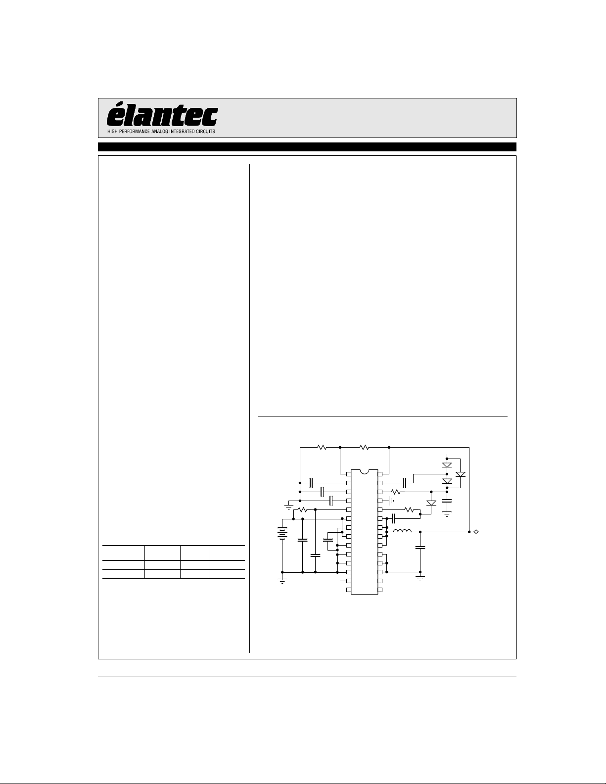
Connection Diagram
C4
R5
5.1Ω
C9
V
IN
660µF
C3
1µF
C12 - 1µF
C3, C4, C5, C6, C7 C8 - ceramic
C5, C11 - ceramic or tantalum
C9 - Sprague 293D337X96R3 2X330µF
C10 - Sprague 293D337X96R3 3X330µF
L1 - Pulse Engineering, PE-53681
D1-D4: BAT54S fast diode
D4 Required for EL7556ACM Only
Manufactured under U.S. Patents No. 5,723,974 and No. 5,793,126
R4 R3
100Ω 150Ω
0.1µF
C7
Connect to VSSP for
external feedback
1
2
39pF
3
C8
220pF
4
5
6
7
C12
8
1µF
9
10
11
12
13
FB1
CREF
C2V
CSLOPE
VSS
COSC
VDD
VIN
VSSP
VIN
VSSP
VSSP
VSSP
VSSP
VSSP
TEST
VSSP
VCC2DET
PWRGD
OUTEN
EL7556BC
28
FB2
CP
VHI
LX
LX
LX
LX
OT
C 5
27
1µF
R1
26
20Ω
25
R6
24
39.2Ω
C 6
23
0.1µF
22
L1
2.5µH
21
20
19
18
17
16
1514
V
IN
D3
D2
D4*
(Optional)
D1
C11
0.22µF
V
OUT =
C10
1mF
1V*(1+R3/R4)
October 5, 2001
Note: All information contained in this data sheet has been carefully checked and is believed to be accurate as of the date of publication; however, this data sheet cannot be a “controlled document”. Current revisions, if any, to these
specifications are maintained at the factory and are available upon your request. We recommend checking the revision level before finalization of your design documentation.
© 2001 Elantec Semiconductor, Inc.
Page 2
EL7556BC
Integrated Adjustable 6 Amp Synchronous Switcher
EL7556BC
Absolute Maximum Ratings (T
Storage Temperature Range -65°C to +150°C
Supply (VIN) 6.0V
Ambient Operating Temperature -40°C to +85°C
= 25°C)
A
Output Pins -0.3V below GND, +0.3V above VDD
Operating Junction Temperature 135°C
Peak Output Current 9A
Important Note:
All parameters having Min/Max specifications are guaranteed. Typ values are for information purposes only. Unless otherwise noted, all tests are at the
specified temperature and are pulsed tests, therefore: TJ = TC = TA.
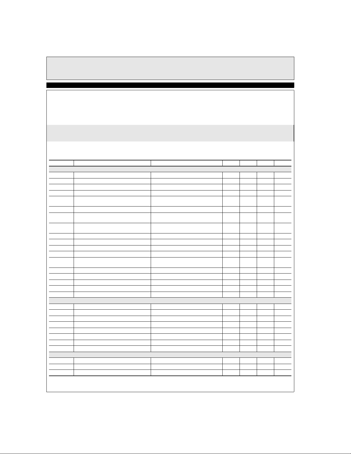
Electrical Characteristics
V
= VIN = 5V, C
DD
Parameter Description Conditions Min Typ Max Unit
General
I
DD
I
DDOFF
I
VIN
V
OUT1
V
OUT2
V
OUTLINE
V
OUTLOAD
R
SHORT
I
I MAX
V
OUTTC
T
OT
T
HYS
V
PWRGD
V
DDOFF
V
DDON
V
HYS
M
SS
D
MAX
Controller - Inputs
I
PUP
I
CSLOPE
I
FB1
R
OT
V
IH
V
IL
VOH
PWGD
V
OL PWGD
Controller - Reference
V
REF
V
REFTC
V
REFLOAD
= 1nF, C
OSC
VDD Supply Current OUTEN = 4V, F
= 470pF, TA = 25°C unless otherwise specified.
SLOPE
= 120kHz 11 25 mA
OSC
VDD Standby Current OUTEN = 0 0.1 mA
V
No Load Current OUTEN = 0 3 5 mA
IN
Output Initial Accuracy VCC2DET = 4V, IL = 3A (See Fig. 1) 3.450 3.500 3.550 V
Output Initial Accuracy VCC2DET = 0V, IL = 3A R
100Ω (See Fig. 1)
= 150Ω, R
3
=
2.450 2.500 2.550 V
4
Output line Regulation VDD = 5V, ±10% -1 1 %
Output Load Regulation 0A<I
Short Circuit Load Resistance IL = 6A, Prior to Continuous Application of
<6A, Relative to IL = 3A. Continu-
LOAD
ous Mode of Operation (See Fig.1)
R
. OUTEN Connected to OT.
SHORT
-1 1 %
100 mΩ
Current Limit 9 A
Output Tempco -40°C<TA<85°C ±1 %
Over Temperature Threshold 135 °C
Over Temperature Hysteresis 40 °C
Power Good Threshold Relative to Programmed
Output Voltage
VCC2SEL = 4V, V
= 3.50V ±6 ±10 ±14 %
OUT
Minimum VDD for Shutdown 3.15 V
Maximum VDD for Startup 4.15 V
Input Hysteresis V
HYS
= V
DDON-VDDOFF
0.5 V
Soft start slope 7 V/mS
Maximum duty cycle 96 %
VCC2DET, OUTEN Pull Up Current VCC2DET, OUTEN = 0 10 14 18 µA
Cslope Charging Current 23 28.5 34 µA
FB1 Input Pull Up Current 2 µA
Over Temperature Pull Up Resistance OT = 0V 30 40 50 kΩ
VCC2DET, OUTEN Input High 4 V
VCC2DET, OUTEN Input Low 0.8 V
Powergood Drive High I
Powergood Drive Low I
Reference Accuracy I
= 1mA 3.5 V
LOAD
= -1mA 1.0 V
LOAD
= 0 1.247 1.260 1.273 V
REF
Reference Voltage Tempco 50 ppm/ºC
Reference Load Regulation 0<I
<100µA 0.5 0.5 %/ºC
LOAD
2
Page 3
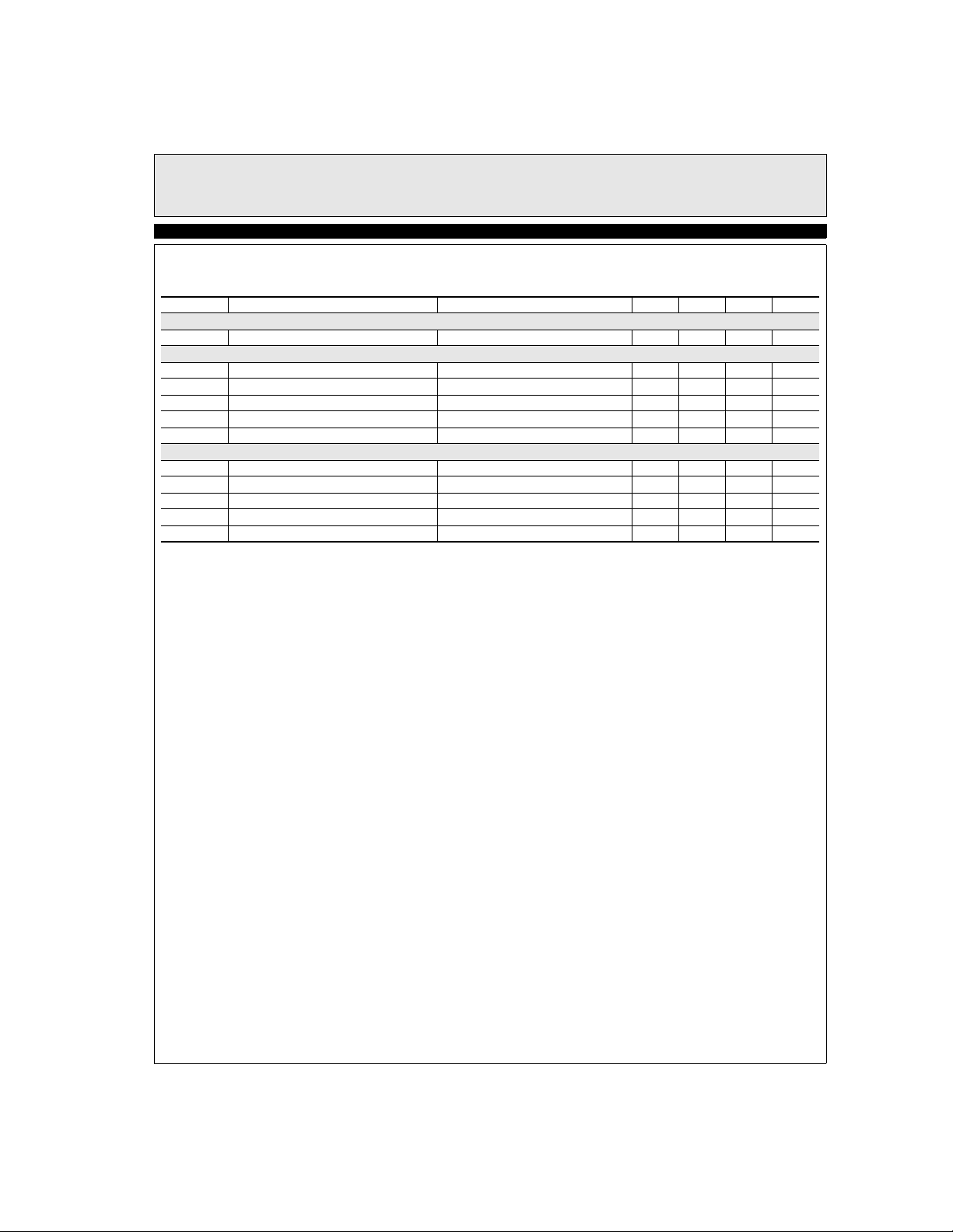
EL7556BC
Integrated Adjustable 6 Amp Synchronous Switcher
Electrical Characteristics
V
= VIN = 5V, C
DD
Parameter Description Conditions Min Typ Max Unit
Controller - Doubler
V
C2V
Controller - Oscillator
F
RAMP
I
OSC CHG
I
OSC DIS
F
OSC
t
SYNC
Power - FET
I
LEAK
R
DSON
R
DSONTC
t
BRM
t
LEB
= 1nF, C
OSC
Voltage Doubler Output V
Oscillator Ramp Amplitude 1.2 V
Oscillator Charge Current 0.2V<V
Oscillator Discharge Current 0.2V<V
Oscillator initial accuracy 100 120 140 kHz
Minimum oscillator sync width 50 ns
LX Output Leakage to VSS LX = 0V 100 µA
Composite FET Resistance 18 30 mΩ
R
Tempco 0.1 mΩ/ºC
DSON
FET break before make delay 10 ns
High side FET minimum on time (LEB) 140 ns
= 470pF, TA = 25°C unless otherwise specified.
SLOPE
DD
= 5V, I
= 10mA 7.5 8.1 8.7 V
LOAD
<1.4V 150 µA
OSC
<1.4V 5 mA
OSC
EL7556BC
3
Page 4
EL7556BC
Integrated Adjustable 6 Amp Synchronous Switcher
EL7556BC
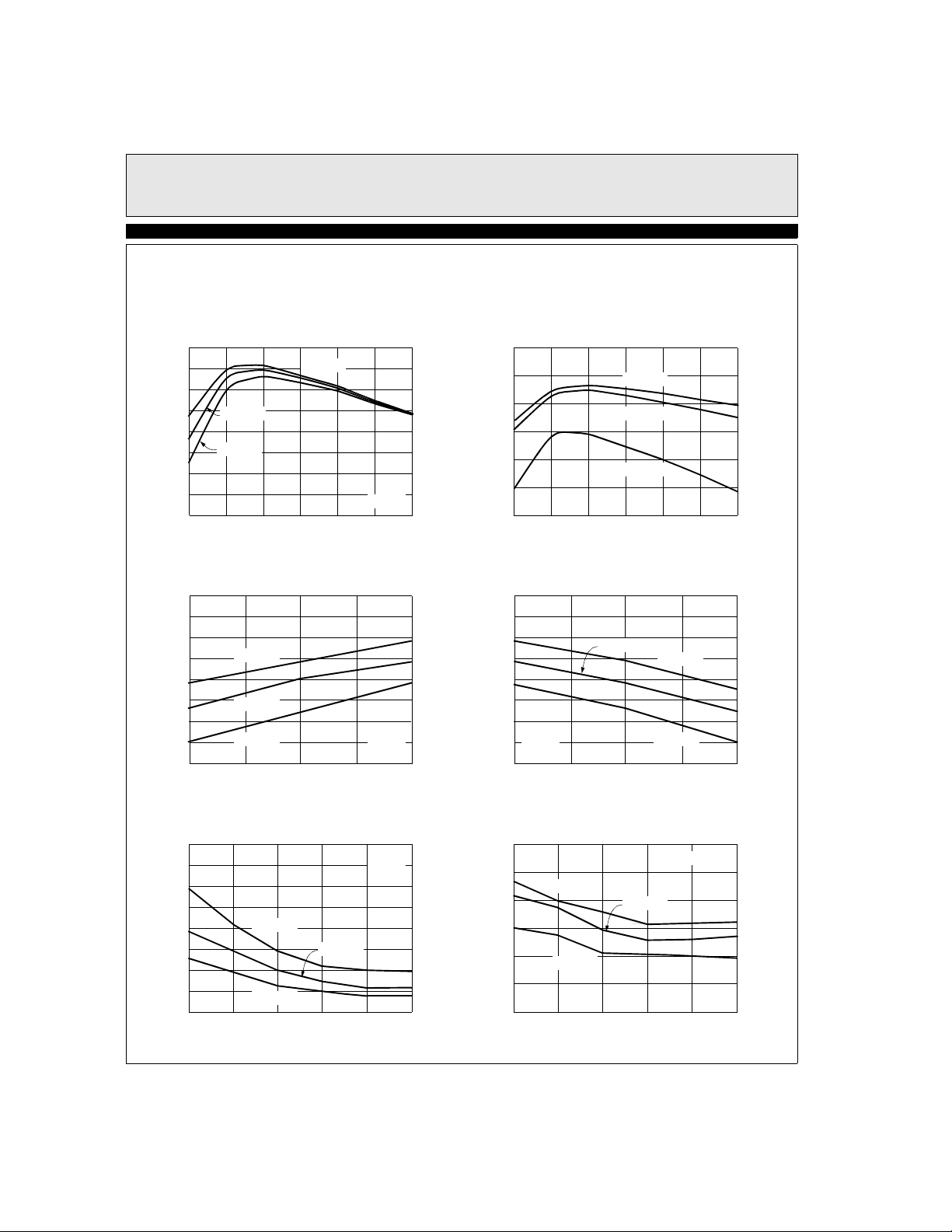
Typical Performance Curves
Efficiency vs I
VDD=VIN=5.0V (±10%)
96
94
LOAD
(V
=3.5V)
OUT
VDD=4.5V
92
90
VDD=5V
88
VDD=5.5V
86
Efficiency (%)
84
82
80
0.5 1.5 2.5 3.5 4.5 5.5
Line Regulation (C
SLOPE
I
OUT
=100pF)
(A)
3.54
3.53
3.52
I
=0.5A
3.51
(V)
3.50
OUT
V
3.49
OUT
I
OUT
=3A
3.48
I
=6A
3.47
3.46
4.5 5.0 5.5
OUT
VIN (V)
TA=25°C
TA=25°C
Efficiency vs I
(VDD=5.0V)
LOAD
100
95
90
VCC=3.5V
VCC=2.5V
85
Efficiency (%)
80
VCC=1V
75
6.5
70
0.5
1.5
Load Regulation (C
2.5 3.5 4.5 6.0
I
(A)
OUT
=100pF)
SLOPE
5.5
3.54
3.53
3.52
3.51
(V)
3.50
OUT
V
3.49
VIN=5V
VIN=5.5V
3.48
OUT
VIN=4.5V
(A)
3.47
TA=25°C
3.46
0.5 3.0 6.0
I
Line Regulation vs C
VDD=VIN=5.0V ±10%
0.8
0.7
0.6
0.5
(±) (%)
0.4
OUT
0.3
∆V
0.2
0.1
0.0
50 75
(I
=3A)
SLOPE
OUT
TA=25°C
V
=3.5A
OUT
V
=2.5A
OUT
V
=1A
OUT
100 125 150 175
C
(pF)
SLOPE
Load Regulation vs C
I
=3A, +3A, -2.5A
OUT
0.6
SLOPE (VIN
=5.0V)
TA=25°C
0.5
V
=3.5A
0.4
(±) (%)
0.3
OUT
∆V
0.2
OUT
V
=2.5A
OUT
V
=1A
OUT
0.1
0.0
50 75 100 125 150 175
C
SLOPE
(pF)
4
Page 5

Typical Performance Curves
EL7556BC
EL7556BC
Integrated Adjustable 6 Amp Synchronous Switcher
Line Regulation vs C
VIN=VDD=5.0V ±10%
0.8
0.7
0.6
0.5
(±) (%)
0.4
OUT
0.3
∆V
0.2
0.1
0.0
50 75
V
(VIN=5.0V, I
1.5
1.0
0.5
0.0
-0.5
(±) (%)
-1.0
OUT
∆V
-1.5
-2.0
-2.5
-3.0
50 75
OUT
SLOPE
TA=25°C
Load Regulation vs C
I
=3A, +3A, -2.5A
OUT
0.8
0.7
SLOPE
TA=25°C
0.6
0.5
I
=6A
OUT
I
=0.5A
OUT
(±) (%)
0.4
OUT
0.3
∆V
0.2
VIN=4.5V
VIN=5.5VVIN=5V
0.1
0.0
50 75
V
Variation vs Programmed Output
OUT
1.5
Voltage [V
IDEAL
=(1+R3/R4)]
100 125 150 175
C
(pF)
SLOPE
vs C
SLOPE
100 125 150 175
C
(pF)
SLOPE
=0.5A)
LOAD
TA=25°C
1.0
C
V
=1V
OUT
V
=2.5V
OUT
V
=3.5V
OUT
TA=25°C
100 125 150 175
C
(pF)
SLOPE
0.5
(%)
OUT
0.0
-0.5
Deviation in V
-1.0
Loop Gain Induced Error
-1.5
1.0 1.5
S
L
O
P
E
=
1
C
0
O
0
S
p
C
=
F
2
2
0
p
F
2.0 2.5 3.0 4.0
V
(V)
IDEAL
3.5
F
520
510
500
490
480
470
vs Temperature
OSC
VDD=4.5V
VDD=5.5V
VDD=5V
F
vs C
OSC
OSC
1000
TA=25°C
1000
(kHz)
100
OSC
F
(kHz)
OSC
F
10
460
1
10
C
(pF)
OSC
100k100 1k
450
20
0
40 60 80 140
100
120
Temperature (°C)
5
Page 6

EL7556BC
Integrated Adjustable 6 Amp Synchronous Switcher
EL7556BC
Typical Performance Curves
I(VDD) + I(VIN) vs F
60
TA=25°C
OUTEN=V
50
40
30
(mA)
Q
I
20
10
0
200 1000400 600 800 200 1000400 600 800
I(VDD) vs F
50
TA=25°C
45
OUTEN=V
40
35
30
25
(mA)
DD
I
20
15
10
5
0
200 1000400 600 800
OSC
OSC
DD
DD
VDD=5.5V
VDD=4.5V
F
(kHz)
OSC
VDD=5.5V
VDD=4.5V
F
(kHz)
OSC
VDD=5V
Continuous ModeDiscontinuous Mode
VDD=5V
(mA)
VIN
I
IN
(mA) + IV
DD
I
I(VIN) vs F
16
TA=25°C
14
OUTEN=V
12
10
8
6
4
2
0
IDD + IVIN vs F
2.0
1.5
1.0
10
OSC
DD
F
(kHz)
OSC
OSC
VDD=5.5V
VDD=4.5V
100 100
F
(kHz)
OSC
VDD=5.5V
VDD=5V
VDD=4.5V
Continuous ModeDiscontinuous Mode
VDD=5V
40
30
20
(mA))
Q
I
10
Power On Reset
TA=25°C
OUTEN=V
0
2.5
DD
3.0
3.5 4.5 5.0
VDD(V)
Minimum Output Voltage vs F
2.3
TJ=120°C
2.1
F
=500k
OSC
4.0
1.9
1.7
(V)
1.5
OUT
V
1.3
1.1
0.9
0.7
OSC
VDD=5.5V
VDD=5V
VDD=4.5V
F
(kHz)
OSC
6
Page 7

Typical Performance Curves
EL7556BC
EL7556BC
Integrated Adjustable 6 Amp Synchronous Switcher
ΘJA vs Cu Area
41
39
37
35
33
(°C/W)
JA
Θ
31
29
27
25
0.00 3.00
R
vs Temperature
DSON
38
36
34
32
30
(m Ω)
28
DSON
R
26
24
22
20
0
Board with no
Components
Board with
Inductor
Bare Cu Area (in2)
Temperature (°C)
Maximum I
7556 Demo Board (31°C/W)
8.0
7.5
7.0
6.5
(A)
6.0
LOAD
I
5.5
5.0
4.5
OUTEN connected to OT
6.004.002.001.00 5.00
125755025 100
4.0
25 50
vs Temperature
LOAD
4535
TA (°C)
100 LFPM
Still Air
55
70604030 65
7
Page 8

EL7556BC
Integrated Adjustable 6 Amp Synchronous Switcher
EL7556BC
Pin Descriptions
I = Input, O = Output, S = Supply
Pin Number Pin Name Pin Type Function
1 FB1 I Voltage feedback pin for the buck regulator. Active when VCC2DET is logic low. Normally connected to exter-
2 CREF I Bandgap reference bypass capacitor. Typically 0.1µF to VSS.
3 CSLOPE I Slope compensation capacitor. Ramp width corresponds to LX duty cycle. C
4 COSC I Oscillator timing capacitor. F
5 VDD S Power Supply for PWM control circuitry. Normally the same potential as VIN.
6 VIN S Power supply for the buck regulator. Connected to the drain of the high-side NMOS FET.
7 VSSP S Ground return for the buck regulator. Connected to the source of the low-side synchronous NMOS FET.
8 VIN S Same as pin 6.
9 VSSP S Same as pin 7.
10 VSSP S Same as pin 7.
11 VSSP S Same as pin 7.
12 VSSP S Same as pin 7.
13 VCC2DET I VCC2DET interface logic input. When driven to logic 1 V
14 OUTEN I The switching regulator output is enabled when logic 1. The reference voltage output operates whenever the
15 OT O Over temperature indicator. Normally high. Pulls low when die temperature exceeds 135°C, returns to the high
16 PWRGD O Power good window comparator output. Logic 1 when regulator output is within ±10% of programmed voltage.
17 TEST I Test pin. Must be connected to VSSP in normal operation.
18 VSSP S Same as pin 7.
19 VSSP S Same as pin 7.
20 LX O Inductor drive pin. High current switching output whose average voltage equals the regulator output voltage.
21 LX O Same as pin 20.
22 LX O Same as pin 20.
23 LX O Same as pin 20.
24 VHI I Gate drive to high-side driver. Bootstrapped from LX with a 0.1µF capacitor.
25 VSS S Ground return for the control circuitry.
26 C2V I Connected to voltage doubler output. Supplies gate drive to the low-side driver.
27 CP O Drives the negative side of charge pump capacitor at one-half the oscillator frequency F
28 FB2 I Voltage feedback pin. Active when VCC2DET is logic 1. Internally preset to V
nal resistor divider between VOUT and GND. A 2µA pull-up current forces VOUT to VSS in the event that
FB1is floating and VCC2DET is inadvertently connected to GND.
1:1.5.
(Hz) can be approximated by: F
OSC
FB1 to determine V
power supply is qualified (VDD>VPOR) regardless of the state of this pin.
state when die temperature has cooled to 100°C.
OUT
: V
= 1.0V*(1+R3/R4).
OUT
to C
SLOPE
(Hz) = 0.0001/C
OSC
= 3.500V. When driven to logic 0 the PWM uses
OUT
OUT
ratio is normally
OSC
. C
OSC
.
OSC
= 3.5V.
OSC
in Farads.
8
Page 9

Block Diagram
EL7556BC
EL7556BC
Integrated Adjustable 6 Amp Synchronous Switcher
Pin 25
PWRGD, Pin 16
CP, Pin 27
C2V, Pin 26
VHI, Pin 24
VDD and VIN,
Pin 5,6,8
LX, Pin 20-23
VSSP, Pin 9-12,
18-19
+
-
SS,
OT, Pin 15
V
V2X
-+-
2-1 MUX
Zero Cross Detect
Q
DELAY
LEB T
-
+
Current
-
+
+
1.26V
Q
R
S
PWM
-
+
Current Limit
Σ
VDD
-
+
4V
S
FF
R
SS
C
SS
R
S
UVLO
-
+
VDD
Over Temp Sensor
R
-
+
FB1, Pin1
FB2, Pin 28
VCCDET, Pin 13
CSLOPE, Pin 3
CREF, Pin 27
OUTEN, Pin 14
COSC, Pin 4
9
Page 10

EL7556BC
Integrated Adjustable 6 Amp Synchronous Switcher
EL7556BC
Applications Information
Circuit Description
General
The EL7556BC is a fixed frequency, current mode controlled DC:DC converter with integrated N-channel
power MOSFETS and a high precision reference. The
device incorporates all of the active circuitry required to
implement a cost effective, user-programmable 6A synchronous buck converter suitable for use in CPU power
supplies. By combining fused-lead packaging technology with an efficient synchronous switching
architecture, high power outputs (21W) can be realized
without the use of discrete external heat sinks.
Theory of Operation
The EL7556BC is composed of 7 major blocks:
1. PWM Controller
2. Output Voltage Mode Select
3. NMOS Power FETS and Drive Circuitry
4. Bandgap Reference
5. Oscillator
6. Temperature Sensor
7. Power Good and Power On Reset
PWM Controller
The EL7556BC regulates output voltage through the use
of current-mode controlled pulse width modulation. The
three main elements in a PWM controller are the feedback loop and reference, a pulse width modulator whose
duty cycle is controlled by the feedback error signal, and
a filter which averages the logic level modulator output.
In a step-down (buck) converter, the feedback loop
forces the time-averaged output of the modulator to
equal the desired output voltage. Unlike pure voltagemode control systems current-mode control utilizes dual
feedback loops to provide both output voltage and
inductor current information to the controller. The voltage loop minimizes DC and transient errors in the output
voltage by adjusting the PWM duty-cycle in response to
changes in line or load conditions. Since the output voltage is equal to the time-average of the modulator output
the relatively large LC time constants found in power
supply applications generally results in low bandwidth
and poor transient response. By directly monitoring
changes in inductor current via a series sense resistor the
controller’s response time is not entirely limited by the
output LC filter and can react more quickly to changes in
line or load conditions. This feed-forward characteristic
also simplifies AC loop compensation since it adds a
zero to the overall loop response. Through proper selection of the current-feedback to voltage-feedback ratio,
the overall loop response will approach a one pole system. The resulting system offers several advantages over
traditional voltage control systems, including simpler
loop compensation, pulse by pulse current limiting,
rapid response to line variation and good load step
response.
The heart of the controller is a triple-input direct summing comparator which sums voltage feedback, current
feedback and slope compensating ramp signals together.
Slope compensation is required to prevent system instability which occurs in current-mode topologies
operating at duty-cycles greater than 50% and is also
used to define the open-loop gain of the overall system.
The compensation ramp amplitude is user adjustable and
is set using a single external capacitor (CSLOPE). Each
comparator input is weighted and determines the load
and line regulation characteristics of the system. Current
feedback is measured by sensing the inductor current
flowing through the high-side switch whenever it is conducting. At the beginning of each oscillator period the
high-side NMOS switch is turned on and CSLOPE
ramps positively from its reset state (VREF potential).
The comparator inputs are gated off for a minimum
period of time (LEB) after the high-side switch is turned
on to allow the system to settle. The Leading Edge
Blanking (LEB) period prevents the detection of erroneous voltages at the comparator inputs due to switching
noise. When programming low regulator output voltages
the LEB delay will limit the maximum operating frequency of the circuit since the LEB will result in a
minimum duty-cycle regardless of the PWM error voltage. This relationship is shown in the performance
curves. If the inductor current exceeds the maximum
current limit (I
), a secondary over-current com-
LMAX
10
Page 11

EL7556BC
Integrated Adjustable 6 Amp Synchronous Switcher
EL7556BC
parator will terminate the high-side switch. If I
LMAX
has not been reached, the regulator output voltage is then
compared to the reference voltage VREF. The resultant
error voltage is summed with the current feedback and
slope compensation ramp. The high-side switch remains
on until all three comparator inputs have summed to
zero, at which time the high-side switch is turned off and
the low-side switch is turned on. In order to eliminate
cross-conduction of the high-side and low-side switches
a 10ns break-before-make delay is incorporated in the
switch driver circuitry. In the continuous mode of operation the low-side switch will remain on until the end of
the oscillator period. In order to improve the low current
efficiency of the EL7556BC, a zero-crossing comparator
senses when the inductor transitions through zero. Turning off the low-side switch at zero inductor current
prevents forward conduction through the internal clamping diodes (LX to VSSP) when the low-side switch turns
off, reducing power dissipation. The output enable
(OUTEN) input allows the regulator output to be disabled by an external logic control signal.
Output Voltage Mode Select
The VCC2DET multiplexes the FB1 and FB2 pins to the
PWM controller. A logic 1 on VCC2DET selects the
FB2 input and forces the output voltage to the internally
programmed value of 3.50V. A logic zero on VCC2DET
selects FB1 and allows the output to be programmed
from 1.0 to 3.8V. In general:
drive for both the high-side and low-side switches is
derived through a charge pump consisting of the CP pin
and external components D1-D3 and C5-C6. The CP
output is a low resistance inverter driven at one-half the
oscillator frequency. This is used in conjunction with
D2-D3 to generate a 7.5V (typical) voltage on the C2V
pin which provides gate drive to the low-side NMOS
switch and associated level shifter. In order to use an
NMOS switch for the high-side drive it is necessary to
drive the gate voltage above the source voltage (LX).
This is accomplished by boot-strapping the VHI pin
above the C2V voltage with capacitor C6 and diode D1.
When the low-side switch is turned on the LX voltage is
close to GND potential and capacitor C6 is charged
through diodes D1-D3 to approximately 6.9V. At the
beginning of the next cycle the high side switch turns on
and the LX pin begins to rise from GND to VDD potential. As the LX pin rises the positive plate of capacitor
C6 follows and eventually reaches a value of approximately 11.2V, for VDD=5V. This voltage is then level
shifted and used to drive the gate of the high-side FET,
via the VHI pin.
Reference
A 1% temperature compensated band gap reference is
integrated in the EL7556BC. The external CREF capacitor acts as the dominant pole of the amplifier and can be
increased in size to maximize transient noise rejection.
A value of 0.1uF is recommended.
R
3
1V 1
× Volt×=
------
+
R
4
V
OUT
However, due to the relatively low open loop gain of the
system, gain errors will occur as the output voltage and
loop-gain are changed. This is shown in the performance
curves. (The output voltage is factory trimmed to minimize error at a 2.50V output). A 2uA pull-up current
from FB1 to VIN forces VOUT to GND in the event that
FB1 is not used and the VCC2DET is inadvertently toggled between the internal and external feedback mode of
operation.
NMOS Power FETS and Drive Circuitry
The EL7556BC integrates low resistance (25mΩ)
NMOS FETS to achieve high efficiency at 6A. Gate
Oscillator
The system clock is generated by an internal relaxation
oscillator with a maximum duty-cycle of approximately
96%. Operating frequency can be adjusted through the
COSC pin or can be driven by an external clock source.
If the oscillator is driven by an external source, care
must be taken in the selection of CSLOPE. Since the
COSC and CSLOPE values determine the open loop
gain of the system, changes to COSC require corresponding changes to CSLOPE in order to maintain a
constant gain ratio. The recommended ratio of COSC to
CSLOPE is 1.5:1
Temperature Sensor
An internal temperature sensor continuously monitors
die temperature. In the event that die temperature
11
Page 12

EL7556BC
Integrated Adjustable 6 Amp Synchronous Switcher
EL7556BC
exceeds the thermal trip-point, the OT pin will output a
logic 0. The upper and lower trip points are set to 135 ºC
and 100ºC respectively. To enable thermal shutdown
this pin should be tied directly to OUTEN. Use of this
feature is recommended during normal operation
Power Good and Power On Reset
During power up the output regulator will be disabled
until VIN reaches a value of approximately 4.0V.
Approximately 500mV of hysteresis is present to eliminate noise induced oscillations.
Under-voltage and over-voltage conditions on the regulator output are detected through an internal window
comparator. A logic 1 on the PWRGD output indicates
that regulated output voltage is within ±10% of the nominally programmed output voltage. Although small, the
typical values of the PWRGD threshold will vary with
changes to external feedback (and resultant loop gain) of
the system. This dependence is shown in the typical performance curves.
If the thermal shutdown pin is connected to OUTEN the
IC will enter thermal shutdown when the maximum
junction temperature is reached. For a thermal shutdown
of 135ºC and power dissipation of 2.2W the ambient
temperature is limited to a maximum value of 67ºC (typical). The ambient temperature range can be extended
with the application of air flow. For example, the addition of 100LFM reduces the thermal resistance by
approximately 15% and can extend the operating ambient to 77ºC (typical). Since the thermal performance of
the IC is heavily dependent on the board layout, the system designer should exercise care during the design
phase to ensure that the IC will operate under the worstcase environmental conditions.
Thermal Management
The EL7556BC utilizes “fused lead” packaging technology in conjunction with the system board layout to
achieve a lower thermal resistance than typically found
in standard 28-pin SO packages. By fusing (or connecting) multiple external leads to the die substrate within
the package, a very conductive heat path to the outside
of the package is created. This conductive heat path
MUST then be connected to a heat sinking area on the
PCB in order to dissipate heat out and away from the
device. The conductive paths for the EL7556BC package are the fused leads: # 7, 9, 10, 11, 12, 18, and 19. If
a sufficient amount of PCB metal area is connected to
the fused package leads, a junction-to-ambient thermal
resistance of approximately 31°C/W can be achieved
(compared to 78°C/W for a standard SO28 package).
The general relationship between PCB heat-sinking
metal area and the thermal resistance for this package is
shown in the Performance Curves section of this data
sheet. It can be readily seen that the thermal resistance
for this package approaches an asymptotic value of
approximately 31°C/W without any airflow. Additional
information can be found in Application Note #8 (Measuring the Thermal Resistance of Power Surface-Mount
Packages).
12
Page 13

EL7556BC
Integrated Adjustable 6 Amp Synchronous Switcher
EL7556BC
General Disclaimer
Specifications contained in this data sheet are in effect as of the publication date shown. Elantec, Inc. reserves the right to make changes in the circuitry or specifications contained herein at any time without notice. Elantec, Inc. assumes no responsibility for the use of any circuits described
herein and makes no representations that they are free from patent infringement.
WARNING - Life Support Policy
Elantec, Inc. products are not authorized for and should not be used
within Life Support Systems without the specific written consent of
Elantec, Inc. Life Support systems are equipment intended to sup-
Elantec Semiconductor, Inc.
675 Trade Zone Blvd.
Milpitas, CA 95035
Telephone: (408) 945-1323
(888) ELANTEC
Fax: (408) 945-9305
European Office: +44-118-977-6020
Japan Technical Center: +81-45-682-5820
port or sustain life and whose failure to perform when properly used
in accordance with instructions provided can be reasonably
expected to result in significant personal injury or death. Users contemplating application of Elantec, Inc. Products in Life Support
Systems are requested to contact Elantec, Inc. factory headquarters
to establish suitable terms & conditions for these applications. Elantec, Inc.’s warranty is limited to replacement of defective
components and does not cover injury to persons or property or
other consequential damages.
October 5, 2001
13
Printed in U.S.A.
 Loading...