

Page 1
®
www.BDTIC.com/Intersil
EL7515
Data Sheet August 10, 2007
High Frequency PWM Step-Up Regulator
The EL7515 is a high frequency, high efficiency step-up
DC/DC regulator operated at fixed frequency PWM mode.
With an integrated 1.4A MOSFET , it can deliver up to 600mA
output current at up to 92% efficiency. The adjustable
switching frequency is up to 1.2MHz, making it ideal for DSL
applications.
When shut down, it draws <1µA of current. This feature,
along with the minimum starting voltage of 1.8V, makes it
suitable for portable equipment powered by one Lithium Ion,
3 to 4 NiMH cells, or 2 cells of alkaline battery.
The EL7515 is available in a 10 Ld MSOP package, with
maximum height of 1.1mm. With proper external
components, the whole converter takes less than 0.25in
2
PCB space.
This device is specified for operation over the full -40°C to
+85°C temperature range.
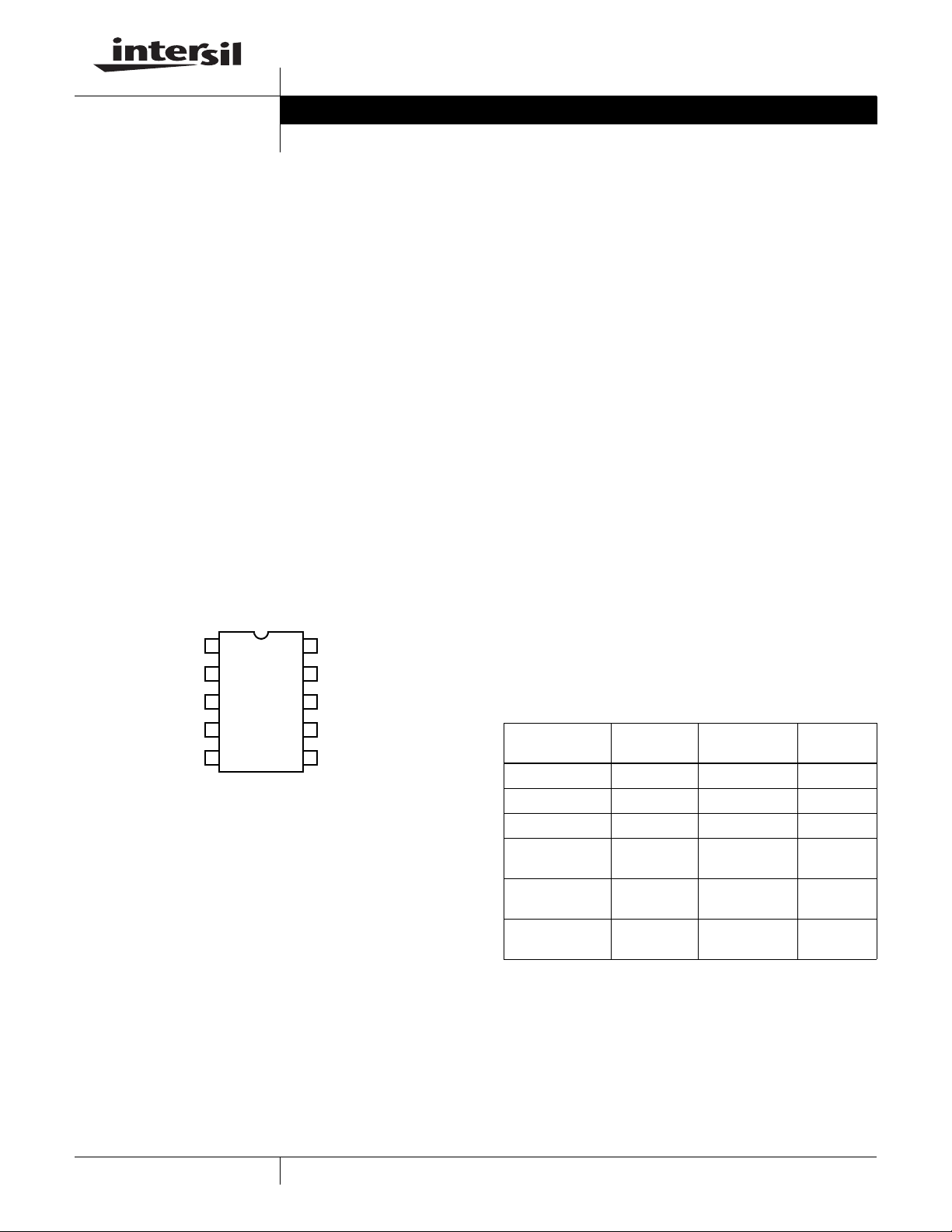
Pinout
EL7515
(10 LD MSOP)
TOP VIEW
PGND
SGND
1
2
LX
10
VDD
9
Features
• Up to 92% efficiency
• Up to 600mA I
•4.5V < V
•1.8V < V
< 17V
OUT
< 13.2V
IN
OUT
• Up to 1.2MHz adjustable frequency
• <1µA shutdown current
• Adjustable soft-start
• Low battery detection
• Internal thermal protection
• 1.1mm max height 10 Ld MSOP package
• Pb-Free available (RoHS compliant)
Applications
• 3V to 5V and 12V converters
• 5V to 12V converters
•TFT-LCD
•DSL
• Portable equipment
• Desktop equipment
FN7120.2
RT
3
EN
4
5 6
FB
8
SS
7
LBOLBI
Ordering Information
PART
NUMBER
EL7515IY e 10 Ld MSOP MDP0043
EL7515IY-T7* e 10 Ld MSOP MDP0043
EL7515IY-T13* e 10 Ld MSOP MDP0043
EL7515IYZ
(Note)
EL7515IYZ-T7*
(Note)
EL7515IYZ-T13*
(Note)
*Please refer to TB347 for details on reel specifications.
NOTE: These Intersil Pb-free plastic packaged products employ
special Pb-free material sets; molding compounds/die attach
materials and 100% matte tin plate PLUS ANNEAL - e3 termination
finish, which is RoHS compliant and compatible with both SnPb and
Pb-free soldering operations. Intersil Pb-free products are MSL
classified at Pb-free peak reflow temperatures that meet or exceed
the Pb-free requirements of IPC/JEDEC J STD-020.
PART
MARKING PACKAGE
BAAAR 10 Ld MSOP
(Pb-free)
BAAAR 10 Ld MSOP
(Pb-free)
BAAAR 10 Ld MSOP
(Pb-free)
PKG.
DWG. #
MDP0043
MDP0043
MDP0043
1
CAUTION: These devices are sensitive to electrostatic discharge; follow proper IC Handling Procedures.
1-888-INTERSIL or 1-888-468-3774
| Intersil (and design) is a registered trademark of Intersil Americas Inc.
Copyright Intersil Americas Inc. 2003, 2005, 2007. All Rights Reserved
All other trademarks mentioned are the property of their respective owners.
Page 2
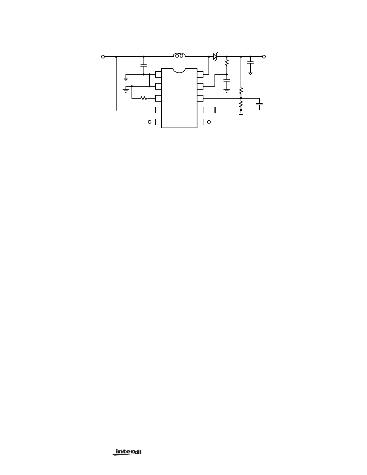
Typical Application
www.BDTIC.com/Intersil
(1.8V TO 9V)
EL7515
L
PGND
SGND
RT
EN
LBI
1
10µH
LX
VDD
FB
SS
LBO
V
IN
C
10µF
1
R
100kΩ
1
2
3
3
4
5 6
D
1
R
4
1.4kΩ
10
9
8
7
20nF
C
4
0.1µF
R
2
82kΩ
R
C
3
1
10kΩ
C
5
22µF
V
OUT
(12V UP TO
630mA)
C
10
4.7nF
2
FN7120.2
August 10, 2007
Page 3

EL7515
www.BDTIC.com/Intersil
Absolute Maximum Ratings (T
EN, LBI, VDD. . . . . . . . . . . . . . . . . . . . . . . . . . . . . . . . . . . . . . .+12V
LX . . . . . . . . . . . . . . . . . . . . . . . . . . . . . . . . . . . . . . . . . . . . . . .+18V
CAUTION: Do not operate at or near the maximum ratings listed for extended periods of time. Exposure to such conditions may adversely impact product reliability and
result in failures not covered by warranty.
IMPORTANT NOTE: All parameters having Min/Max specifications are guaranteed. Typ values are for informati on purposes only. Unless otherwise noted, all tests are
at the specified temperature and are pulsed tests, therefore: T
Electrical Specifications V
PARAMETER DESCRIPTION CONDITIONS
V
IN
V
OUT
IQ1 Quiescent Current - Shut-down V
IQ2 Quiescent Current V
V
FB
IB Feedback Input Bias Current 0.10 µA
D
MAX
I
LIM
I
SHDN
V
LBI
V
OL-LBO
I
LEAK-LBO
r
DS(ON)
I
LEAK-SWITCH
/ΔVIN/V
ΔV
OUT
ΔV
OUT/VOUT
f
OSC-MAX
f
OSC1
VHI_EN EN Input High Threshold 1.6 V
VLO_EN EN Input Low Threshold 0.5 V
Input Voltage Range 1.8 13.2 V
Output Voltage Range 4.5 17 V
Feedback Voltage 1.29 1.33 1.37 V
Maximum Duty Cycle 84 90 %
Current Limit - Max Peak Input
Current
Shut-down Input Bias Current 1µA
LBI Threshold Voltage 180 220 250 mV
LBO Output Low I
LBO Output Leakage Current V
Switch On Resistance at 12V output 220 mΩ
Switch Leakage Current 1µA
Line Regulation 3V < V
OUT
Load Regulation I
Maximum Switching Frequency RT = 49.9kΩ 1200 kHz
Switching Frequency 600 670 750 kHz
= +25°C) Thermal Information
A
Storage Temperature. . . . . . . . . . . . . . . . . . . . . . . .-65°C to +150°C
Operating Temperature . . . . . . . . . . . . . . . . . . . . . . .-40°C to +85°C
Operating Junction Temperature: . . . . . . . . . . . . . . . . . . . . .+135°C
Pb-free reflow profile . . . . . . . . . . . . . . . . . . . . . . . . . .see link below
http://www.intersil.com/pbfree/Pb-FreeReflow.asp
= TC = T
IN
= 5V, V
J
= 12V, L = 10µH, I
OUT
A
= 0mA, RT = 100kΩ, TA = +25°C, Unless Otherwise Specified.
OUT
= 0, feedback resistors disconnected 1 µA
EN
= 2V 1.4 2 mA
EN
= 1mA 0.1 0.2 V
LBO
= 250mV, V
LBI
< 6V, V
IN
= 50mA to 150mA 1 %
OUT
= 5V 0.02 2 µA
LBO
= 12V, no load 0.4 %/V
OUT
MIN
(Note 1) TYP
11.4 A
MAX
(Note 1) UNIT
Pin Descriptions
PIN NUMBER PIN NAME PIN FUNCTION
1 PGND Power ground; connected to the source of internal N-Channel power MOSFET
2 SGND Signal ground; ground reference for all the control circuitry; needs to have only a single connection to PGND
3 RT Timing resistor to adjust the oscillation frequency of the converter
4 EN Chip enable; connects to logic HI (>1.6V) for chip to function
5 LBI Low battery input; connects to a sensing voltage, or left open if function is not used
6 LBO Low battery detection output; connected to the open drain of a MOSFET; able to sink 1mA current
7 SS Soft-start; connects to a capacitor to control the start-up of the converter
8 FB Voltage feedback input; needs to connect to resistor divider to decide V
9 VDD Control circuit positive supply
10 LX Inductor drive pin; connected to the drain of internal N-Channel power MOSFET
3
O
FN7120.2
August 10, 2007
Page 4
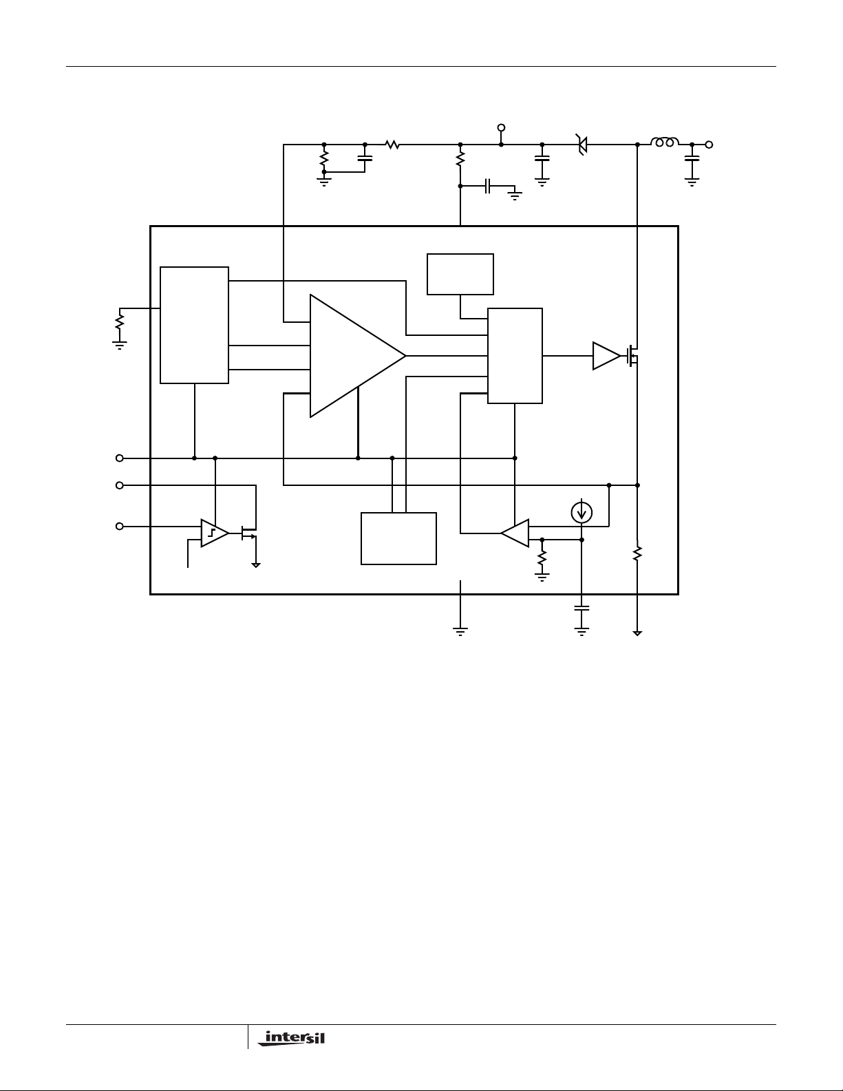
Block Diagram
www.BDTIC.com/Intersil
10kΩ
4.7nF
EL7515
82kΩ
1.4kΩ
0.1µF
V
OUT
22µF
10µA
10µF
V
IN
100kΩ
R
EN
LBO
LBI
T
REFERENCE
GENERATOR
+
220mV
FB V
MAX_DUTY
V
V
RAMP
REF
PWM
COMPARATOR
START-UP
OSCILLATOR
DD
THERMAL
SHUT-DOWN
PWM
LOGIC
-
+
I
LOUT
SGND PGNDSS
7.2kΩ
LX
0.2Ω
12µA
80mΩ
20nF
4
FN7120.2
August 10, 2007
Page 5
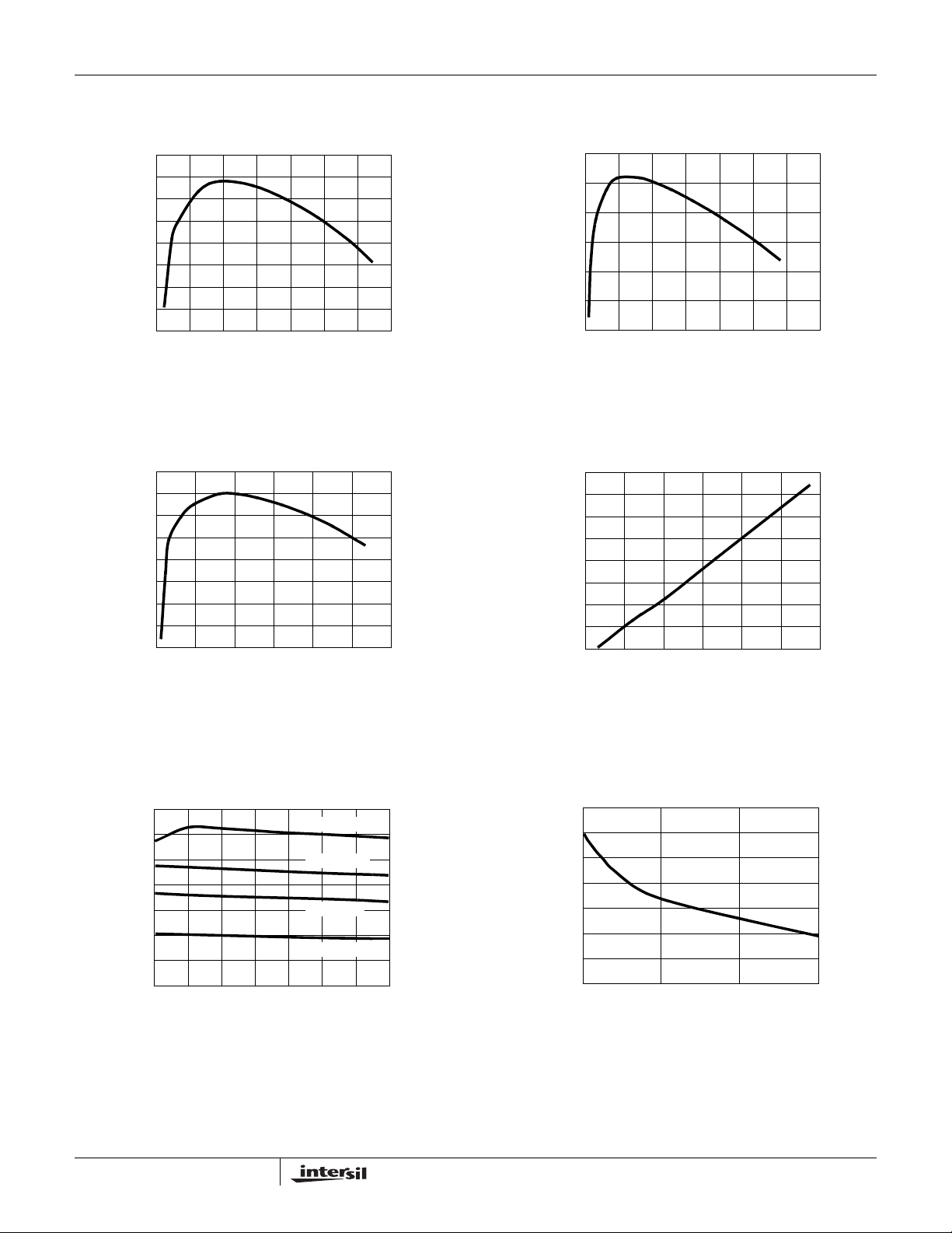
Typical Performance Curves
www.BDTIC.com/Intersil
V
= 3.3V, VO = 12V
IN
92
90
88
86
84
82
EFFICIENCY (%)
80
78
76
0 50 100 150 200 250 300 350
(mA)
I
OUT
FIGURE 1. EFFICIENCY vs I
V
= 5V, VO = 12V
IN
94
92
90
88
86
84
EFFICIENCY (%)
82
80
78
0 100 200 300 400 500 600
(mA)
I
OUT
FIGURE 3. EFFICIENCY vs I
OUT
OUT
EL7515
V
= 3.3V, VO = 5V
IN
92
90
88
86
84
EFFICIENCY (%)
82
80
0 100 200 300 400 500 600 700
(mA)
I
OUT
FIGURE 2. EFFICIENCY vs I
V
= 10V, VO = 12V TO 17V
DD
2.2
2.1
2
1.9
1.8
(mA)
DD
I
1.7
1.6
1.5
1.4
650 750 850 950 1050 1150 1250
(kHz)
F
S
FIGURE 4. IDD vs F
OUT
S
V
1400
1200
1000
800
(kHz)
S
600
F
400
200
0
56 9 12
710811
V
FIGURE 5. FS vs V
DD
RT = 51.1kΩ
RT = 71.5kΩ
RT = 100kΩ
RT = 200kΩ
(V)
DD
1400
1200
1000
800
(kHz)
S
600
F
400
200
0
50 100 150 200
5
= 10V
DD
FIGURE 6. FS vs R
(kΩ)
R
T
T
FN7120.2
August 10, 2007
Page 6
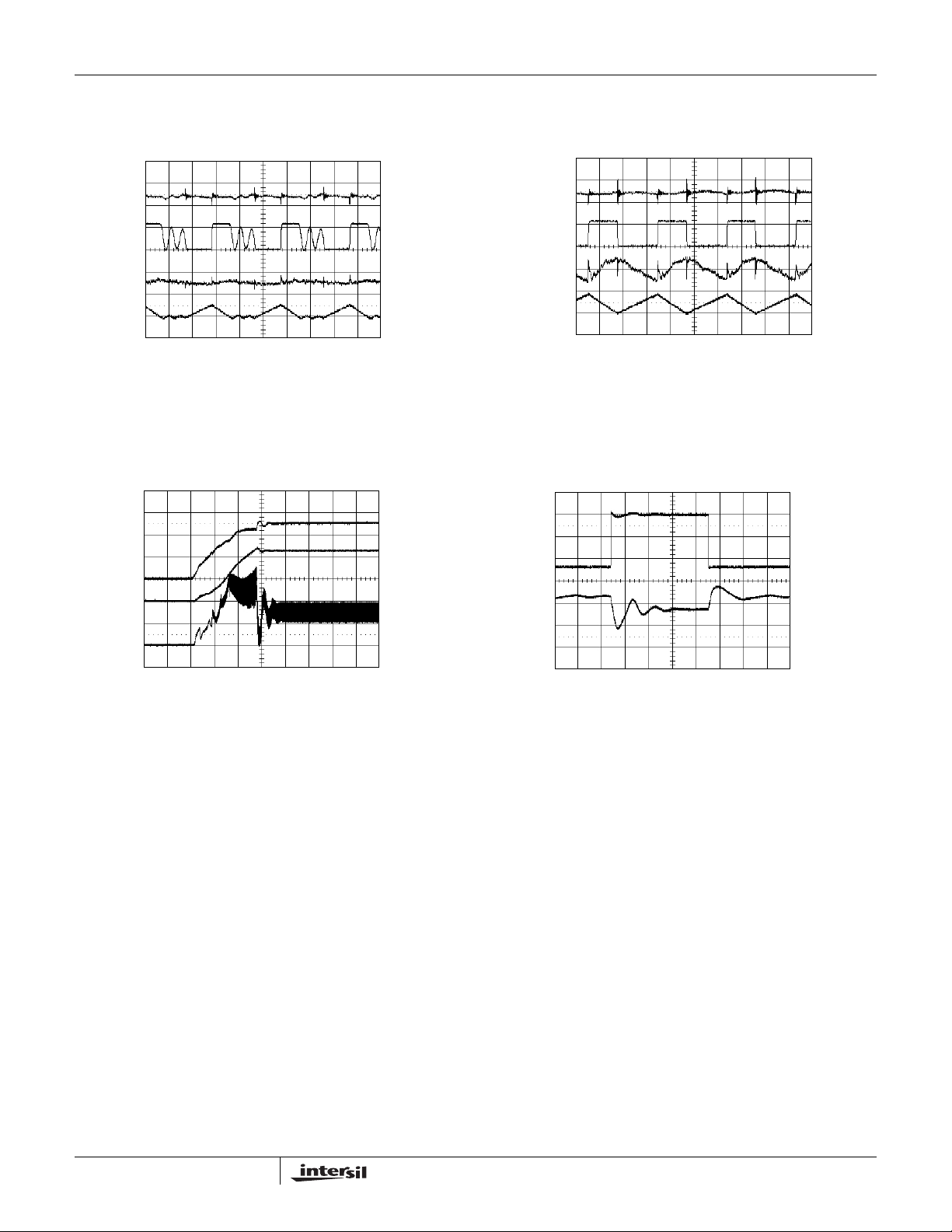
Typical Performance Curves (Continued)
www.BDTIC.com/Intersil
V
= 5V, VO = 12V, IO = 30mA
IN
EL7515
V
= 5V, VO = 12V, IO = 300mA
IN
ΔV
IN
V
LX
ΔV
O
I
L
0.5µs/DIV
FIGURE 7. STEADY STA TE OPERA TION (INDUCTOR
DISCONTINUOUS CONDUCTION)
V
= 5V, VO = 12V, IO = 300mA
IN
ΔV
IN
V
O
I
L
50mV/DIV
10V/DIV
20mV/DIV
0.5A/DIV
2V/DIV
5V/DIV
0.5A/DIV
ΔV
IN
V
LX
ΔV
O
I
L
0.5µs/DIV
FIGURE 8. STEADY STA TE OPERATION (INDUCTOR
I
ΔV
CONTINUOUS CONDUCTION)
V
= 5V, VO = 12V, IO = 50mA TO 300mA
IN
O
O
50mV/DIV
10V/DIV
20mV/DIV
0.5A/DIV
100mA/DIV
0.5V/DIV
0.5ms/DIV
FIGURE 9. POWER-UP
Applications Information
The EL7515 is a step-up regulator, operated at fixed
frequency pulse-width-modulation (PWM) control. The input
voltage is 1.8V to 13.2V and output voltage is 4.5V to 17V.
The switching frequency (up to 1.2MHz) is decided by the
resistor connected to R
Start-Up
After VDD reaches a threshold of about 1.7V, the start-up
oscillator generates fixed duty-ratio of 0.5 to 0.7 at a
frequency of several hundred kilohertz. This will boost the
output voltage.
When V
over the control. The duty ratio will be decided by the
multiple-input direct summing comparator, Max_Duty signal
(about 90% duty-ratio), and the Current Limit Comparator,
whichever is the smallest.
The soft-start is provided by the current limit comparator. As
the internal 12µA current source charges the external CSS,
the peak MOSFET current is limited by the voltage on the
reaches about 3.7V, the PWM comparator takes
DD
pin.
T
0.2ms/DIV
FIGURE 10. LOAD TRANSIENT RESPONSE
capacitor. This in turn controls the rising rate of the output
voltage.
The regulator goes through the start-up sequence as well
after the EN signal is pulled to HI.
Steady-State Operation
When the output reaches the preset voltage, the regulator
operates at steady state. Depending on the input/output
conditions and component values, the inductor operates at
either continuous-conduction mode or
discontinuous-conduction mode.
In the continuous-conduction mode, the inductor current is a
triangular waveform and LX voltage a pulse waveform. In the
discontinuous-conduction mode, the inductor current is
completely dried out before the MOSFET is turned on again.
The input voltage source, the inductor, and the MOSFET and
output diode parasitic capacitors form a resonant circuit.
Oscillation will occur in this period. This oscillation is normal
and will not affect the regulation.
6
FN7120.2
August 10, 2007
Page 7
)
EL7515
www.BDTIC.com/Intersil
At very low load, the MOSFET will skip pulses sometimes.
This is normal.
Current Limit
The MOSFET current limit is nominally 1.4A and guaranteed
1A. This restricts the maximum output current I
on Equation 1:
V
ΔI
L
I
OMAX
⎛⎞
1
⎝⎠
IN
--------–
---------×=
2
V
O
where:
• ΔIL is the inductor peak-to-peak current ripple and is
decided by Equation 2:
V
D
ΔI
IN
---- -×=
---------
L
L
f
S
• D is the MOSFET turn-on ratio and is decided by
Equation 3:
–
V
OVIN
----------------------- -=
D
V
O
is the switching frequency
•f
S
The following table gives typical values:
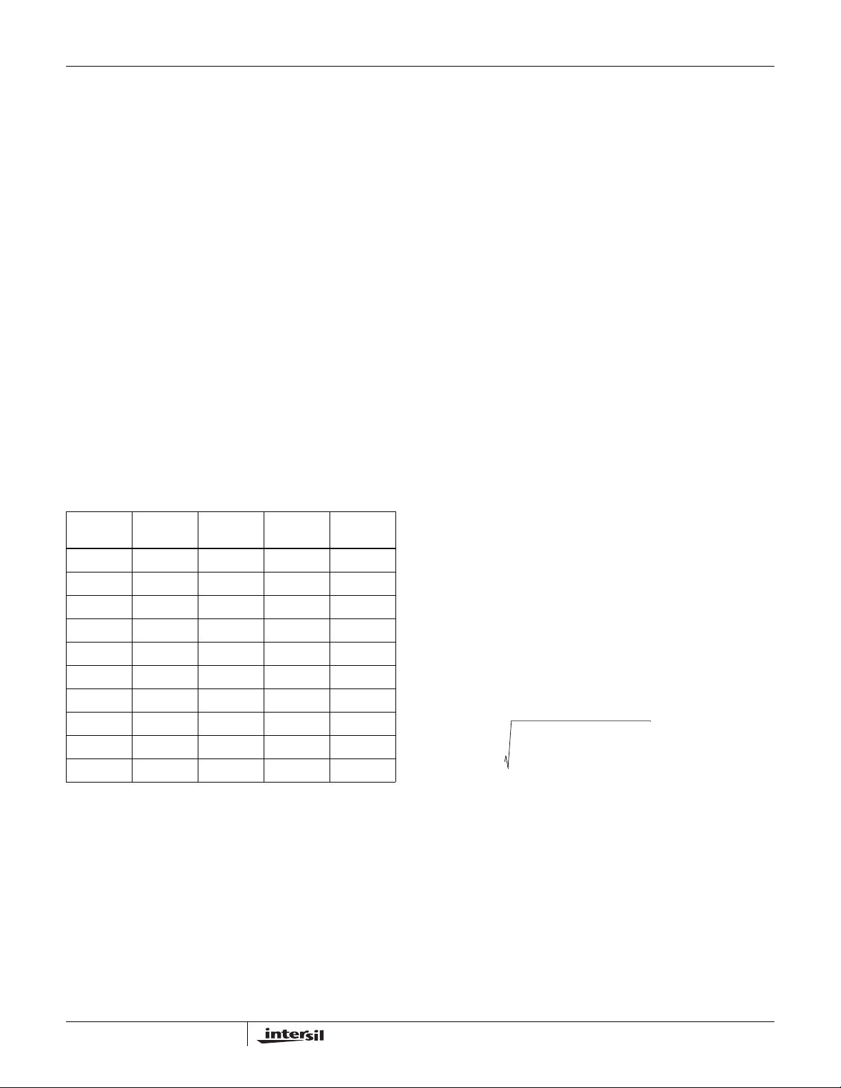
TABLE 1. MAX CONTINUOUS OUTPUT CURRENTS
V
IN
(V)
2 5 10 1000 360
2 9 10 1000 190
2 12 10 1000 140
3.3 5 10 1000 600
3.3 9 10 1000 310
3.3 12 10 1000 230
5 9 10 1000 470
5 12 10 1000 340
9 12 10 1000 630
12 15 10 100 670
V
(V)
O
L
(µH)
F
S
(kHz)
OMAX
based
(EQ. 1
(EQ. 2)
(EQ. 3)
I
OMAX
(mA)
The inductor has peak and average current decided by
Equations 4 and 5:
I
LPKILAVG
I
LAVG
-------------=
1D–
L
--------+=
2
I
O
(EQ. 4)
(EQ. 5)
ΔI
The inductor should be chosen to be able to handle this
current. Furthermore, due to the fixed internal
compensation, it is recommended that maximum inductance
of 10µH and 15µH to be used in the 5V and 12V or higher
output voltage, respectively.
The output diode has an average current of I
, and peak
O
current the same as the inductor's peak current. A Schottky
diode is recommended and it should be able to handle those
currents.
The output voltage ripple can be calculated as Equation 6:
ΔV
O
IOD×
---------------------- I
×
F
SCO
LPK
ESR×+=
(EQ. 6)
Where:
•C
is the output capacitance.
O
• The ESR is the output capacitor ESR value.
Low ESR capacitors should be used to minimize the output
voltage ripple. Multilayer ceramic capacitors (X5R and X7R)
are preferred for the output capacitors since they have a low
ESR and small packages. Tantalum capacitors also can be
used, but they take more board space and have higher ESR.
A minimum of 22µF output capacitor is sufficient for high
output current application. For lower output current, the
output capacitor can be smaller, like 4.7µF. The capacitor
should always have enough voltage rating. In addition to the
voltage rating, the output capacitor should also be able to
handle the RMS current which is given by Equation 7:
2
I
CORMS
⎛
ΔI
------------------- -+
I
LAVG
L
1( D ) D
⎜
⎝
⎜
– I
×
⎞
1
⎟
------×
×=
LAVG
⎟
2
12
⎠
(EQ. 7)
Component Considerations
It is recommended that CIN is larger than 10µF.
Theoretically, the input capacitor has a ripple current of ΔI
Due to high-frequency noise in the circuit, the input current
ripple may exceed the theoretical value. A larger capacitor
will reduce the ripple further.
7
.
L
An external resistor divider is required to divide the output
voltage down to the nominal reference voltage. The current
drawn by the resistor network should be limited to maintain
the overall converter efficiency. The maximum value of the
resistor network is limited by the feedback input bias current
and the potential for noise being coupled into the feedback
pin. A resistor network less than 300kΩ is recommended.
Output Voltage
FN7120.2
August 10, 2007
Page 8

EL7515
www.BDTIC.com/Intersil
The boost converter output voltage is determined by the
relationship in Equation 8:
V
OUTVFB
where V
2
×=
1
-------+
⎜⎟
R
⎝⎠
1
slightly changes with VDD. The curve is shown in
FB
(EQ. 8)
R
⎛⎞
this data sheet.
RC Filter
The maximum voltage rating for the VDD pin is 12V and is
recommended to be about 10V for maximum efficiency to
drive the internal MOSFET. The series resistor R
filter connected to V
If V
is larger than 10V, then Equation 9 shows:
O
VO10–
R
-------------------- -=
4
I
DD
can be utilized to reduce the voltage.
DD
in the RC
4
(EQ. 9)
where IDD is shown in IDD vs fS curve. Otherwise, R4 can be
10Ω to 51Ω with C
= 0.1µF.
4
Thermal Performance
The EL7515 uses a fused-lead package, which has a
reduced θ
+115°C/W on a two-layer board. Maximizing copper around
the ground pins will improve the thermal performance.
of +100°C/W on a four-layer board and
JA
Layout Considerations
The layout is very important for the converter to function
properly. Power Ground ( ) and Signal Ground ( ) should
be separated to ensure that the high pulse current in the
Power Ground never interferes with the sensitive signals
connected to Signal Ground. They should only be connected
at one point.
The trace connected to pin 8 (FB) is the most sensitive trace.
It needs to be as short as possible and in a “quiet” place,
preferably between PGND or SGND traces.
In addition, the bypass capacitor connected to the VDD pin
needs to be as close to the pin as possible.
The heat of the chip is mainly dissipated through the SGND
pin. Maximizing the copper area around it is preferable. In
addition, a solid ground plane is always helpful for the EMI
performance.
The demo board is a good example of layout based on these
principles. Please refer to the EL7515 Application Brief for
the layout. http://www.intersil.com/data/tb/tb429.pdf
This chip also has internal thermal shut-down set at around
+135°C to protect the component.
8
FN7120.2
August 10, 2007
Page 9
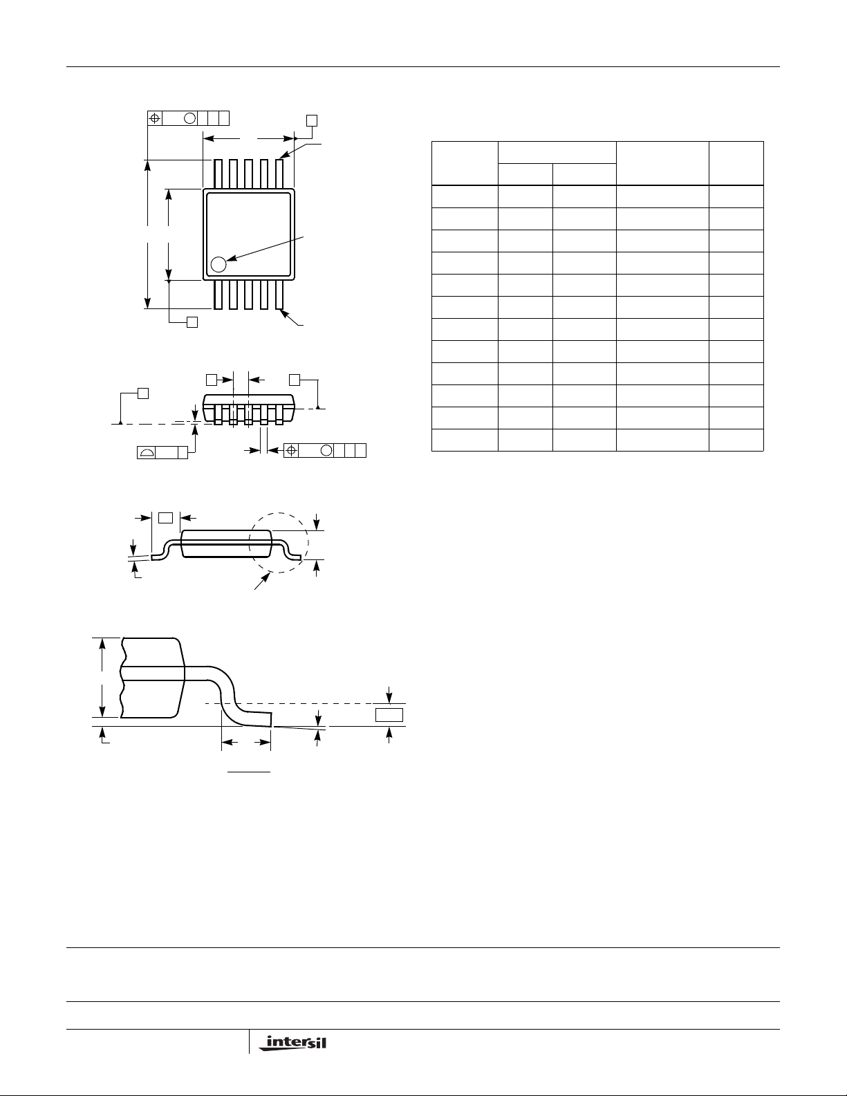
Mini SO Package Family (MSOP)
www.BDTIC.com/Intersil
M
C
SEATING
PLANE
N LEADS
c
0.25 C A B
E1E
B
0.10 C
L1
SEE DETAIL "X"
D
N
1
e
b
A
(N/2)+1
PIN #1
I.D.
(N/2)
H
M
0.08 C A B
A
EL7515
MDP0043
MINI SO PACKAGE FAMILY
SYMBOL
A1.101.10 Max. A1 0.10 0.10 ±0.05 A2 0.86 0.86 ±0.09 -
b 0.33 0.23 +0.07/-0.08 -
c0.180.18 ±0.05 -
D 3.00 3.00 ±0.10 1, 3
E4.904.90 ±0.15 E1 3.00 3.00 ±0.10 2, 3
e0.650.50 Basic -
L0.550.55 ±0.15 L1 0.95 0.95 Basic -
N 8 10 Reference -
NOTES:
1. Plastic or metal protrusions of 0.15mm maximum per side are not
included.
2. Plastic interlead protrusions of 0.25mm maximum per side are
not included.
3. Dimensions “D” and “E1” are measured at Datum Plane “H”.
4. Dimensioning and tolerancing per ASME Y14.5M-1994.
MILLIMETERS
TOLERANCE NOTESMSOP8 MSOP10
Rev. D 2/07
A2
GAUGE
A1
L
DETAIL X
PLANE
3° ±3°
0.25
All Intersil U.S. products are manufactured, assembled and tested utilizing ISO9000 quality systems.
Intersil Corporation’s quality certifications can be viewed at www.intersil.com/design/quality
Intersil products are sold by description only. Intersil Corporation reserves the right to make changes in circuit design, software and/or specifications at any time without
notice. Accordingly, the reader is cautioned to verify that data sheets are current before placing orders. Information furnished by Intersil is believed to be accurate and
reliable. However, no responsibility is assumed by Intersil or its subsidiaries for its use; nor for any infringements of patents or other rights of third parties which may result
from its use. No license is granted by implic atio n or other wise u nde r any p a tent or patent rights of Intersil or its subsidi ari es.
For information regarding Intersil Corporation and its products, see www.intersil.com
9
FN7120.2
August 10, 2007
 Loading...