

Datasheet EL7513IY-T7, EL7513IY-T13, EL7513IY, EL7513IWT-T7, EL7513IWT Datasheet (Intersil Corporation)
Page 1
1
®
FN7112.2
EL7513
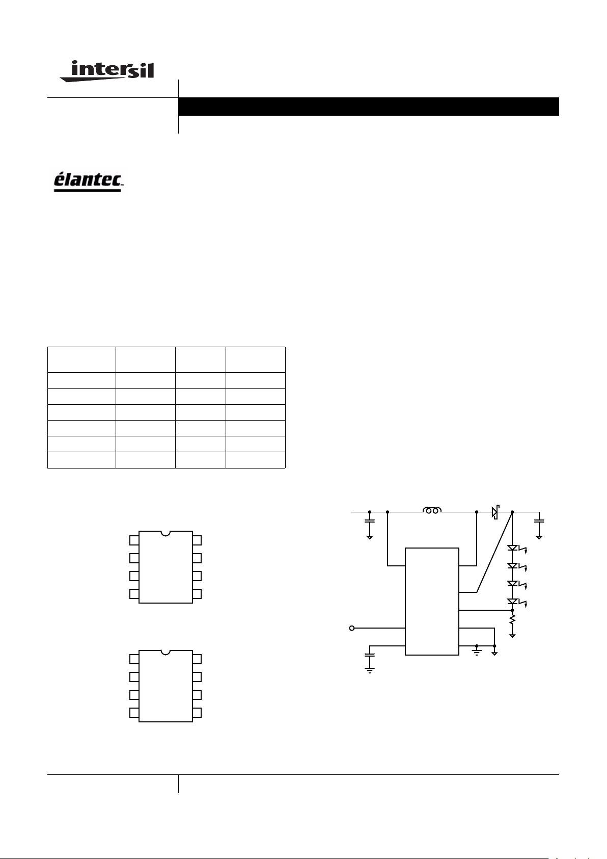
White LED Step-Up Regulator
The EL7513 is a constant current
boost regulator specially designed for
driving white LEDs. It can drive 4
LEDs in series or up to 12 LEDs in parallel/series
configuration and achieves efficiency up to 91%.
The brightness of the LEDs is adjusted through a voltage
level on the CNTL pin. When the level falls below 0.1V, the
chip goes into shut-down mode and consumes less than
1µA of supply current for V
IN
less than 5.5V.
The EL7513 is available in the 8-pin TSOT and 8-pin MSOP
packages. The TSOT package is just 1mm high, compared
to 1.45mm for the standard SOT23 package.
Features
• 2.6V to 13.2V input voltage
• 18V maximum output voltage
• Drives up to 12 LEDs
• 1MHz switching frequency
• Up to 91% efficiency
• 1µA maximum shut-down current
• Dimming control
• 8-pin TSOT and 8-pin MSOP packages
Applications
•PDAs
• Cellular phones
• Digital cameras
• White LED backlighting
Ordering Information
PAR T
NUMBER PACKAGE
TAPE &
REEL PKG. DWG. #
EL7513IWT 8-Pin TSOT - MDP0049
EL7513IWT-T7 8-Pin TSOT 7” MDP0049
EL7513IWT-T13 8-Pin TSOT 13” MDP0049
EL7513IY 8-Pin MSOP - MDP0043
EL7513IY-T7 8-Pin MSOP 7” MDP0043
EL7513IY-T13 8-Pin MSOP 13” MDP0043
Pinouts Typical Connection
EL7513
(8-PIN TSOT)
TOP VIEW
EL7513
(8-PIN MSOP)
TOP VIEW
COMP
CNTL
VOUT
LX
VIN
CS
SGND
PGND
1
2
3
4
8
7
6
5
CS
VIN
PGND
SGND
CNTL
COMP
LX
VOUT
1
2
3
4
8
7
6
5
C
1
LXVIN
VOUT
CS
PGND
SGND
CNTL
COMP
4.7µF
C
3
0.1µF
C
2
1µF
L
33µH
D
2.6V TO
5.5V
R
1
V
CTRL
5Ω
Data Sheet July 2003
CAUTION: These devices are sensitive to electrostatic discharge; follow proper IC Handling Procedures.
1-888-INTERSIL or 321-724-7143
| Intersil (and design) is a registered trademark of Intersil Americas Inc.
Copyright © Intersil Americas Inc. 2003. All Rights Reserved. Elantec is a registered trademark of Elantec Semiconductor, Inc.
All other trademarks mentioned are the property of their respective owners.
Page 2
2
IMPORTANT NOTE: All parameters having Min/Max specifications are guaranteed. Typ values are for information purposes only. Unless otherwise noted, all tests are
at the specified temperature and are pulsed tests, therefore: T
J
= TC = T
A
Absolute Maximum Ratings (T
A
= 25°C)
COMP, CNTL, CS to SGND. . . . . . . . . . . . . . . . . . . . . . -0.3V to +6V
V
IN
to SGND . . . . . . . . . . . . . . . . . . . . . . . . . . . . . . . . . . . . . . .+14V
V
OUT
to SGND . . . . . . . . . . . . . . . . . . . . . . . . . . . . . . . . . . . . .+19V
LX to PGND . . . . . . . . . . . . . . . . . . . . . . . . . . . . . . . . . . . . . . . .+20V
SGND to PGND . . . . . . . . . . . . . . . . . . . . . . . . . . . . . -0.3V to +0.3V
Storage Temperature . . . . . . . . . . . . . . . . . . . . . . . . -65°C to +150°C
Ambient Operating Temperature . . . . . . . . . . . . . . . . -40°C to +85°C
CAUTION: Stresses above those listed in “Absolute Maximum Ratings” may cause permanent damage to the device. This is a stress only rating and operation of the
device at these or any other conditions above those indicated in the operational sections of this specification is not implied. This part is ESD sensitive. Handle with care.
Electrical Specifications V
IN
= 3V, VO = 12V, C1 = 4.7µF, L = 33µH, C2 = 1µF, C3 = 0.1µF, R1 = 5Ω, TA = 25°C,
Unless Otherwise Specified
PARAMETER DESCRIPTION CONDITIONS MIN TYP MAX UNIT
V
IN
Input Voltage 2.6 13.2 V
I
Q1
Total Input Current at Shut-down V
CNTL
= 0V 1 µA
I
Q1
Quiescent Supply Current at VO Pin V
CNTL
= 1V, load disconnected 1 1.5 mA
I
COMP
COMP Pin Pull-up Current COMP connected to SGND 11 20 µA
V
COMP
COMP Voltage Swing 0.5 1.5 2.5 V
I
CNTL
CNTL Shut-down Current CNTL = 0V 1 µA
V
CNTL1
Chip Enable Voltage 240 mV
V
CNTL2
Chip Disable Voltage 100 mV
I
OUT_ACCURACYVCNTL
= 1V V
CNTL
= 1V 14 15 16 mA
V
OUT1
Over-voltage Threshold V
OUT
rising 17 18 19 V
V
OUT2
Over-voltage Threshold V
OUT
falling, with resistive load 15 16 17.5 V
ILX MOSFET Current Limit 500 mA
R
DS_ON
MOSFET On-resistance 0.7 Ω
I
LEAK
MOSFET Leakage Current V
CNTL
= 0V, VLX = 12V 1 µA
F
S
Switching Frequency 800 1000 1200 kHz
D
MAX
Maximum Duty Ratio V
CNTL
= 2V, IS = 0 85 90 %
I
CS
CS Input Bias Current 1µA
∆I
O
/∆V
IN
Line Regulation VIN = 2.6V - 5.5V 0.03 %/V
Pin Descriptions
8-PIN TSOT 8-PIN MSOP PIN NAME DESCRIPTION
1 7 COMP Compensation pin. A compensation cap (4700pF to 1µF) is normally connected between this pin and
SGND.
2 8 CNTL Control pin for dimming and shut-down. A voltage between 250mV and 5.5V controls the brightness,
and less than 100mV shuts down the converter.
3 5 VOUT Output voltage sense. Use for over voltage protection.
4 6 LX Inductor connection pin. The drain of internal MOSFET.
5 3 PGND Power Ground pin. The source of internal MOSFET.
6 4 SGND Signal Ground. Ground pin for internal control circuitry. Needs to connect to PGND at only one point.
7 1 CS Current sense pin. Connect to sensing resistor to set the LED bias current.
8 2 VIN Power supply for internal control circuitry.
EL7513
Page 3
3
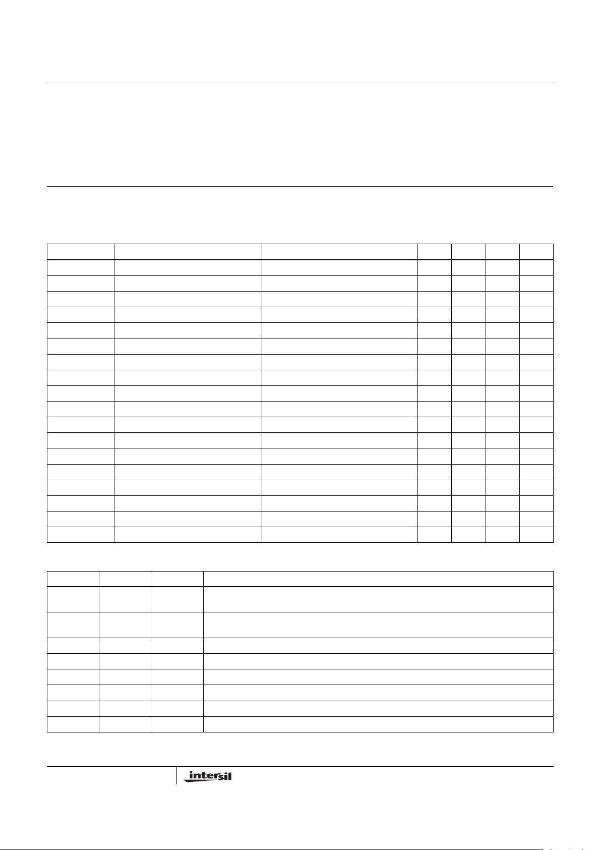
Block Diagram
REFERENCE
GENERATOR
1MHz
OSCILLATOR
THERMAL
SHUTDOWN
BOOST
I-SENSE
START-UP
CONTROL
+
+
-
+
+
PWM
SIGNAL
C
OUT
1µF
I(LED)
OVER-VOLTAGE
PROTECTION
ERROR AMP
CNTL
COMP
V
IN
C
IN
4.7µF
C
COMP
0.1µF
SGND
C
S
PGND
LX
V
OUT
L
33µH
2.6V TO
5.5V
5Ω
V
CNTL
PWM
LOGIC
617K
50K
Typical Performance Curves
All performance curves and waveforms are taken with C1 = 4.7µF, C2 = 1µF, C3 = 0.1µF, L = 33µF, V
IN
= 3.3V, V
CNTL
= 1V, R1=5Ω, 4 LEDs in a
series; unless otherwise specified.
FIGURE 1. SWITCHING FREQUENCY vs V
IN
FIGURE 2. QUIESCENT CURRENT
1.05
1.04
1.02
1.01
1
2.5 3.5 4.5
V
IN
(V)
F
S
(MHz)
1.03
5.5345
3.5
2
1
0
2.5 6.5 10.5
V
IN
(V)
I
IN
(µA)
3
14.54.5 8.5 12.5
2.5
1.5
0.5
V
CNTL
=0V, 0.1V
WHITE LEDs DISCONNECTED
EL7513
Page 4
4
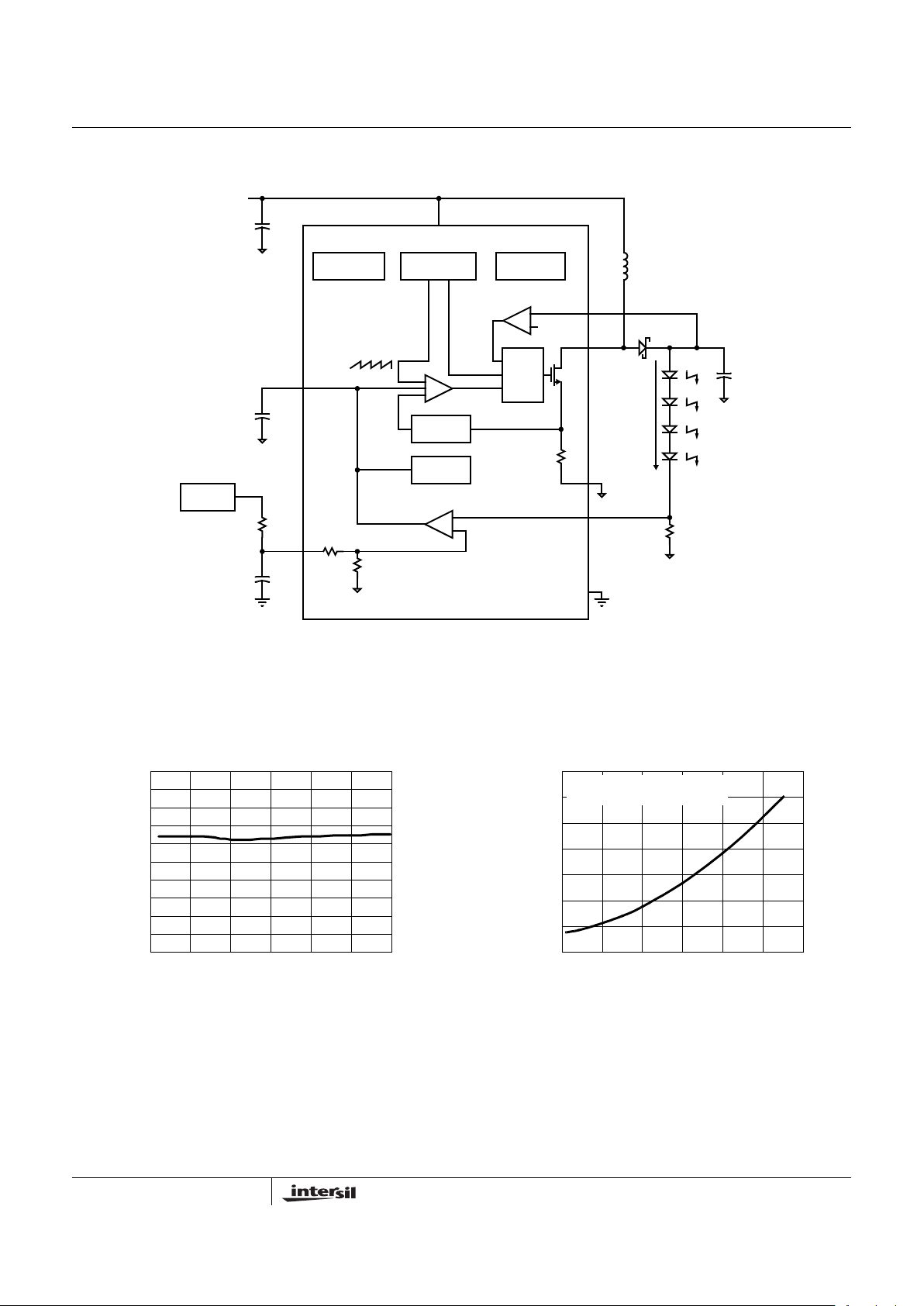
FIGURE 3. I
LED
vs V
CNTL
FIGURE 4. I
LED
vs V
IN
FIGURE 5A. 2 LEDs IN A SERIES FIGURE 5B. EFFICIENCY vs I
O
FIGURE 5.
FIGURE 6A. 3 LEDs IN A SERIES FIGURE 6B. EFFICIENCY vs I
O
FIGURE 6.
Typical Performance Curves (Continued)
All performance curves and waveforms are taken with C
1
= 4.7µF, C2 = 1µF, C3 = 0.1µF, L = 33µF, V
IN
= 3.3V, V
CNTL
= 1V, R1=5Ω, 4 LEDs in a
series; unless otherwise specified.
0
5
10
15
20
25
30
35
0 0.5 1 1.5 2 2.5
V
CNTL
(V)
I
LED
(mA)
14
14.2
14.4
14.6
14.8
15
15.2
15.4
15.6
15.8
16
2.53.54.55.5
V
IN
(V)
V
CNTL
=1V
I
LED
(mA)
34
5
LXVIN
VOUT
CS
PGND
SGND
CNTL
COMP
4.7µF
0.1µF
1µF
L
33µH
BAT54HT1
V
IN
25
16
3
7
48
V
CTRL
5Ω
2 LEDs IN A SERIES
90
85
80
75
70
5 1015202530
I
O
(mA)
EFFICIENCY (%)
L=COILCRAFT LPO1704-333CM
VIN=4.2V
VIN=2.7V
LXVIN
VOUT
CS
PGND
SGND
CNTL
COMP
4.7µF
0.1µF
1µF
L
33µH
BAT54HT1
V
IN
25
16
3
7
48
V
CTRL
5Ω
3 LEDs IN A SERIES
90
85
80
75
70
5 1015202530
I
O
(mA)
EFFICIENCY (%)
L=COILCRAFT LPO1704-333CM
VIN=4.2V
VIN=2.7V
EL7513
Page 5

5
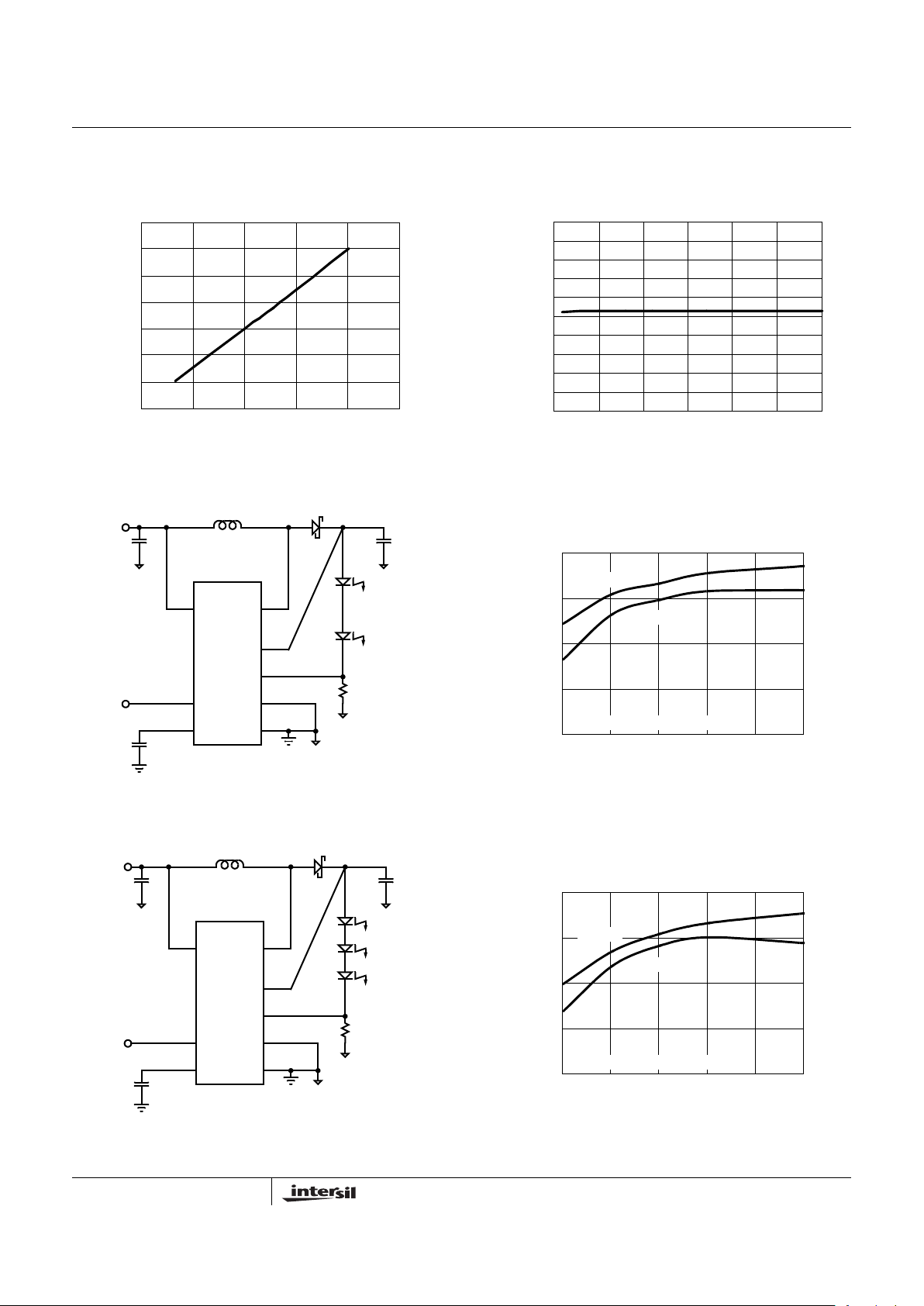
FIGURE 7A. 4 LEDs IN A SERIES FIGURE 7B. EFFICIENCY vs I
O
FIGURE 7.
FIGURE 8A. 2 LEGS OF 2 LEDs IN A SERIES FIGURE 8B. EFFICIENCY vs I
O
FIGURE 8.
FIGURE 9A. 2 LEGS OF 3 LEDs IN A SERIES FIGURE 9B. EFFICIENCY vs I
O
FIGURE 9.
Typical Performance Curves (Continued)
All performance curves and waveforms are taken with C
1
= 4.7µF, C2 = 1µF, C3 = 0.1µF, L = 33µF, V
IN
= 3.3V, V
CNTL
= 1V, R1=5Ω, 4 LEDs in a
series; unless otherwise specified.
LXVIN
VOUT
CS
PGND
SGND
CNTL
COMP
4.7µF
0.1µF
1µF
L
33µH
BAT54HT1
V
IN
25
16
3
7
48
V
CTRL
5Ω
4 LEDs IN A SERIES
90
85
80
75
70
5 1015202530
LED CURRENT (mA)
EFFICIENCY (%)
L=COILCRAFT LPO1704-333CM
VIN=4.2V
VIN=2.7V
VIN=3.3V
LXVIN
VOUT
CS
PGND
SGND
CNTL
COMP
4.7µF
0.1µF
1µF
L
33µH
BAT54HT1
V
IN
25
16
3
7
48
V
CTRL
5Ω 5Ω
2 LEGS OF 2 LEDs IN A SERIES
90
85
80
75
70
10 20 30 40 50 60
I
O
(mA)
EFFICIENCY (%)
L=COILCRAFT LPO1704-333CM
VIN=4.2V
VIN=2.7V
LXVIN
VOUT
CS
PGND
SGND
CNTL
COMP
4.7µF
0.1µF
1µF
L
33µH
BAT54HT1
V
IN
25
16
3
7
48
V
CTRL
5Ω 5Ω
2 LEGS OF 3 LEDs IN A SERIES
90
85
80
75
70
10 20 30 40 50 60
I
O
(mA)
EFFICIENCY (%)
L=SUMIDA CMD13D13-33µH
VIN=4.2V
VIN=2.7V
EL7513
Page 6

6
FIGURE 10A. 2 LEGS OF 4 LEDs IN A SERIES FIGURE 10B. EFFICIENCY vs I
O
FIGURE 10.
FIGURE 11A. 3 LEGS OF 2 LEDs IN A SERIES FIGURE 11B. EFFICIENCY vs I
O
FIGURE 11.
FIGURE 12A. 3 LEGS OF 3 LEDs IN A SERIES FIGURE 12B. EFFICIENCY vs I
O
FIGURE 12.
Typical Performance Curves (Continued)
All performance curves and waveforms are taken with C
1
= 4.7µF, C2 = 1µF, C3 = 0.1µF, L = 33µF, V
IN
= 3.3V, V
CNTL
= 1V, R1=5Ω, 4 LEDs in a
series; unless otherwise specified.
LXVIN
VOUT
CS
PGND
SGND
CNTL
COMP
4.7µF
0.1µF
1µF
L
33µH
BAT54HT1
V
IN
25
16
3
7
48
V
CTRL
5Ω 5Ω
2 LEGS OF 4 LEDs IN A SERIES
90
85
80
75
70
10 20 30 40 50 60
I
O
(mA)
EFFICIENCY (%)
L=SUMIDA CMD13D13-
VIN=4.2V
VIN=2.7V
LXVIN
VOUT
CS
PGND
SGND
CNTL
COMP
4.7µF
0.1µF
1µF
L
15µH
BAT54HT1
V
IN
25
16
3
7
48
V
CTRL
5Ω 5Ω 5Ω
3 LEGS OF 2 LEDs IN A SERIES
95
90
80
75
70
15 35 55 75
I
O
(mA)
EFFICIENCY (%)
L=SUMIDA CMD13D13-15µH
VIN=4.2V
VIN=2.7V
85
95
LXVIN
VOUT
CS
PGND
SGND
CNTL
COMP
4.7µF
0.1µF
1µF
L
15µH
BAT54HT1
V
IN
25
16
3
7
48
V
CTRL
5Ω 5Ω 5Ω
3 LEGS OF 3 LEDs IN A SERIES
95
90
80
75
70
15 35 55 75
I
O
(mA)
EFFICIENCY (%)
L=SUMIDA CMD13D13-15µH
VIN=4.2V
VIN=2.7V
85
95
EL7513
Page 7

7
FIGURE 13A. 3 LEGS of 4 LEDs in a SERIES FIGURE 13B. EFFICIENCY vs I
O
FIGURE 13.
Typical Performance Curves (Continued)
All performance curves and waveforms are taken with C
1
= 4.7µF, C2 = 1µF, C3 = 0.1µF, L = 33µF, V
IN
= 3.3V, V
CNTL
= 1V, R1=5Ω, 4 LEDs in a
series; unless otherwise specified.
LXVIN
VOUT
CS
PGND
SGND
CNTL
COMP
4.7µF
0.1µF
1µF
L
15µH
BAT54HT1
V
IN
25
16
3
7
48
V
CTRL
5Ω 5Ω 5Ω
3 LEGS OF 4 LEDs IN A SERIES
95
90
80
75
70
15 35 55 75
I
O
(mA)
EFFICIENCY (%)
L=SUMIDA CMD13D13-15µH
VIN=4.2V
VIN=2.7V
85
95
Waveforms
All performance curves and waveforms are taken with C1 = 4.7µF, C2 = 1µF, C3 = 0.1µF, L = 33µF, V
IN
= 3.3V, V
CNTL
= 1V, R1=5Ω, 4 LEDs in a
series; unless otherwise specified.
FIGURE 14. START-UP FIGURE 15. SHUT-DOWN
FIGURE 16. TRANSIENT RESPONSE FIGURE 17. CONTINUOUS CONDUCTION MODE
V
IN
I
IN
V
CNTL
I
LED
2V/DIV
50mA/DIV
1V/DIV
10mA/DIV
10ms/DIV
C3=4700pF
V
CNTL
I
LED
50mA/DIV
1V/DIV
10mA/DIV
I
IN
0.1ms/DIV
V
O
V
CNTL
I
LED
2V
1V
14.2V
12.9V
30mA
15mA
20ms/DIV
I
LED
=15mA
∆V
IN
I
L
V
LX
∆V
O
10mV/DIV
100mA/DIV
10V/DIV
50mV/DIV
1µs/DIV
EL7513
Page 8

8
Detailed Description
The EL7513 is a constant current boost regulator specially
designed for driving white LEDs. It can drive up to 4 LEDs in
series or 12 LEDs in parallel/series configuration and
achieves efficiency up to 91%.
The brightness of the LEDs is adjusted through a voltage
level on the CNTL pin. When the level falls below 0.1V, the
chip goes into shut-down mode and consumes less than
1µA of current for V
IN
less than 5.5V.
Steady-State Operation
EL7513 is operated in constant frequency PWM. The
switching is around 1MHz. Depending on the input voltage,
the inductance, the type of LEDs driven, and the LED’s
current, the converter operates at either continuous
conduction mode or discontinuous conduction mode (see
waveforms). Both are normal.
Brightness Control
LED’s current is controlled by the voltage level on CNTL pin
(V
CNTL
). This voltage can be either a DC or a PWM signal
with frequency less than 200Hz (for C
3
=4700pF). When a
higher frequency PWM is used, an RC filter is recommended
before the CNTL pin (see Figure 20).
The relationship between the LED current and CNTL voltage
level is as follows:
When R
1
is 5Ω, 1V of V
CNTL
conveniently sets I
LED
to
15mA. The range of V
CNTL
is 250mV to 5.5V.
Shut-Down
When V
CNTL
is less than 100mV, the converter is in shutdown mode. The max current consumed by the chip is less
than 1µA for V
IN
less than 5.5V.
Over-Voltage Protection
When an LED string is disconnected from the output, VO will
continue to rise because of no current feedback. When V
O
reaches 18V (nominal), the chip will shut down. The output
voltage will drop. When V
O
drops below 16V (nominal), the
chip will boost output voltage again until it reaches 18V. This
hiccough continues until LED is applied or converter is shut
down.
When designing the converter, caution should be taken to
ensure the highest operating LED voltage does not exceed
17V, the minimum shut-down voltage. There is no external
component required for this function.
Component Selection
The input and output capacitors are not very important for
the converter to operate normally. The input capacitance
is normally 0.22µF - 4.7µF and output capacitance
0.22µF - 1µF. Higher capacitance is allowed to reduce the
voltage/current ripple, but at added cost. Use X5R or X7R
type (for its good temperature characteristics) of ceramic
capacitors with correct voltage rating and maximum height.
FIGURE 18. DISCONTINUOUS CONDUCTION MODE FIGURE 19. OVER VOLTAGE PROTECTION (LED
DISCONNECTED)
Waveforms (Continued)
All performance curves and waveforms are taken with C
1
= 4.7µF, C2 = 1µF, C3 = 0.1µF, L = 33µF, V
IN
= 3.3V, V
CNTL
= 1V, R1=5Ω, 4 LEDs in a
series; unless otherwise specified.
V
CTRL
=0.34V, I
LED
=5mA
∆V
IN
I
L
V
LX
∆V
O
10mV/DIV
100mA/DIV
10V/DIV
50mV/DIV
1µs/DIV
VO (5V/DIV)
V
COMP
(1V/DIV)
FIGURE 20. PWM BRIGHTNESS CONTROL
CNTL
COMP
PWM
SIGNAL
0.1µF
100K
I
LED
V
CNTL
13.33 R
1
×
----------------------------=
EL7513
Page 9

9
When choosing an inductor, make sure the inductor can
handle the average and peak currents giving by following
formulas (80% efficiency assumed):
where:
• ∆I
L
is the peak-to-peak inductor current ripple in Ampere
• L inductance in µH
• FS switching frequency, typical 1MHz
A wide range of inductance (6.8µH - 68µH) can be used for
the converter to function correctly. For the same series of
inductors, the lower inductance has lower DC resistance
(DCR), which has less conducting loss. But the ripple current
is bigger, which generates more RMS current loss. Figure 11
shows the efficiency of the demo board under different
inductance for a specific series of inductor. For optimal
efficiency in an application, it is a good exercise to check
several adjacent inductance values of your preferred series
of inductors.
For the same inductance, higher overall efficiency can be
obtained by using lower DCR inductor.
The diode should be Schottky type with minimum reverse
voltage of 20V. The diode's peak current is the same as
inductor's peak current, the average current is I
O
, and RMS
current is:
Ensure the diode's ratings exceed these current
requirements.
White LED Connections
One leg of LEDs connected in series will ensure the
uniformity of the brightness. 18V maximum voltage enables
4 LEDs can be placed in series.
However, placing LEDs into series/parallel connection can
give higher efficiency as shown in the efficiency curves. One
of the ways to ensure the brightness uniformity is to prescreen the LEDs.
PCB Layout Considerations
The layout is very important for the converter to function
properly. Power Ground ( ) and Signal Ground ( ) should
be separated to ensure the high pulse current in the power
ground does not interference with the sensitive signals
connected to Signal Ground. Both grounds should only be
connected at one point right at the chip. The heavy current
paths (V
IN
-L-LX pin-PGND, and VIN-L-D-C2-PGND) should
be as short as possible.
The trace connected to the CS pin is most important. The
current sense resister R
1
should be very close to the pin
When the trace is long, use a small filter capacitor close to
the CS pin.
The heat of the IC is mainly dissipated through the PGND
pin. Maximizing the copper area around the plane is
preferable. In addition, a solid ground plane is always helpful
for the EMI performance.
The demo board is a good example of layout based on the
principle. Please refer to the EL7513 Application Brief for the
layout.
I
LAVG
IOV
O
×
0.8 V
IN
×
------------------------=
I
LPKILAVG
1
2
-- -
∆I
L
×+=
∆I
L
VINVOVIN–()×
LV
OFS
××
---------------------------------------------=
EFFICIENCY vs I
O
VIN=3.3V FOR
DIFFERENT L
L=Coilcraft
LPO1704 SERIES
1mm HEIGHT
85
83
81
79
77
5 1015202530
I
O
(mA)
EFFICIENCY (%)
L=33µH
L=22µH
L=10µH
L=15µH
FIGURE 21. EFFICIENCY OF DIFFERENT INDUCTANCE
(4 LEDs IN A SERIES)
I
DRMSILAVGIO
×=
EL7513
Page 10

10
Package Outline Drawing
NOTE: The package drawing shown here may not be the latest version. To check the latest revision, please refer to the Intersil website at
<http://www.intersil.com/design/packages/index.asp>
EL7513
Page 11

11
All Intersil U.S. products are manufactured, assembled and tested utilizing ISO9000 quality systems.
Intersil Corporation’s quality certifications can be viewed at www.intersil.com/design/quality
Intersil products are sold by description only. Intersil Corporation reserves the right to make changes in circuit design, software and/or specifications at any time without
notice. Accordingly, the reader is cautioned to verify that data sheets are current before placing orders. Information furnished by Intersil is believed to be accurate and
reliable. However, no responsibility is assumed by Intersil or its subsidiaries for its use; nor for any infringements of patents or other rights of third parties which may result
from its use. No license is granted by implication or otherwise under any patent or patent rights of Intersil or its subsidiaries.
For information regarding Intersil Corporation and its products, see www.intersil.com
Package Outline Drawing
NOTE: The package drawing shown here may not be the latest version. To check the latest revision, please refer to the Intersil website at
<http://www.intersil.com/design/packages/index.asp>
EL7513
 Loading...