

Page 1
EL7457C
40MHz Non-Inverting Quad CMOS Driver
EL7457C
Features
• Clocking Speeds Up To 40MHz
• 4 Channels
• 12 ns tr/tf at 1000 pF Cload
• 1ns Rise and Fall Time Mismatch
• 1.5ns Prop Delay Mismatch
• Low Quiescent Current, <1mA
• Fast Output Enable Function, 12ns
• Wide Output Voltage Range
• 8V >
VL >-5V
• -2V <
VH < 15V
• 2A Peak Drive
• 3Ω On Resistance
• Input Level Shifters
• TTL/CMOS Input Compatible
Applications
• CCD Drivers
• Digital Cameras
• Pin Drivers
• Clock / Line Drivers
• Ultrasound Transducer Drivers
• Ultrasonic and RF Generators
• Level Shifting
General Description
The EL7457C is an ultra-high speed, non-inverting quad CMOS
driver. It is capable of running at clock rates up to 40MHz and features
2A peak drive capability and a nominal on-resistance of just 3Ω. The
EL7457C is ideal for driving highly capacitive loads, such as storage
and vertical clocks in CCD applications. It is also well suited to ATE
pin driving, level-s h iftin g and clock-driving ap pl ic ations.
The EL7457C is capable of running from si ngle or dual power su pplies while using ground referenced inputs. Each output can be
switched to either the high (VH) or low (VL) supply pins, depending
on the related input pin. The inputs are compatible with both 3V and
5V CMOS and TTL logi c. The outp ut en ab le (OE) pin can b e u sed to
put the outputs into a high-impedance state. This is especially useful in
CCD applications, where the driver should be disabled during power
down.
The EL7457C also features very fast rise and fall times which are
matched to within 1ns. The pro pagation de lay is also match ed between
rising and falling edges to within 2ns.
The EL7457C is available in both the 16-Pin QSOP and 16-Pin SOIC
packages. It is specified for operation over the -40°C to +85°C temperature rang e.
Ordering Information
Part No. Temp. Range Package Outline #
EL7457CU -40°C to +85°C 16-Pin QSOP MDP0040 EL7457CS -40°C to +85°C 16-Pin SO MDP0027
© 1998 Élantec, Inc.
Pin Layout Diagram
INA
1
OE
2
3
INB
VL
4
5
GND
NC
6
INC OUTD
7
IND
8 9
EL7457C
VS+
16
OUTA
15
OUTB
14
NC
13
VH
12
OUTC
11
10
VS-
December 7, 1999
Page 2
EL7457C
40MHz Non-Inverting Quad CMOS Driver
EL7457C
Absolute Maximum Ratings (T
Absolute maximum ratings are those values b eyond whic h the device
could be permanently damaged. Absolute maximum ratings are stress
ratings only and functional device operation is not implied.
Supply Voltage (V
Input Voltage GND -0.3V, V
+ to GND) +16.5V
S
= 25°C)
A
+ +0.3V
S
Continuous Output Current 100mA
Storage Temperature Range -65°C to +150°C
Ambient Operating Temperature -40°C to +85°C
Operating Junction Temperature 125°C
Power Dissipation: See Curves
Maximum ESD 2kV
Important Note:
All parameters having Min/Max specifications are guaranteed. Typ values are for information purposes only. Unless otherwise noted, all tests are at the
specified temperature and are pulsed tests, therefore: T
= TC = TA.
J
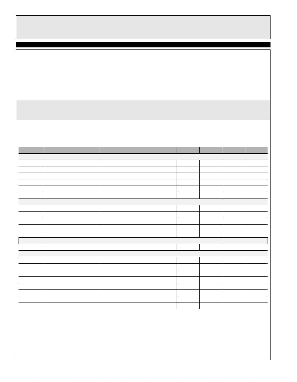
Electrical Characteristics
VS+ = +5V, VS- = -5V, VH = +5V, VL = -5V, TA = 25°C, unless otherwise specified
Parameter Description Condition Min Typ Max Units
Input
V
IH
I
IH
V
IL
I
IL
C
in
R
in
Output
R
OV1
R
OV2
I
Leak
I
PK
Power Supply
I
S
Switching Characteristics
t
R
t
F
t
RFdelta
t
D-1
t
D-2
t
Ddelta
T
enable
T
disable
Logic “1” Input Voltage 2.0 V Logic “1” Input Current VIH = 5V 0.1 10 µA Logic “0” Input Voltage 0.8 V Logic “0” Input Current VIL = 0V 0.1 10 µA
Input Capacitance 3.5 pF
Input Resistance 50 MΩ
ON Resistance VH to OUTx I ON Resistance VL to OUTx I
= -100mA 4.5 6 Ω
OUT
= +100mA 4 6 Ω
OUT
Output Leakage Current VH = VS+, VL = VS-0.110µA
Peak Output Current Source 2.0 A
Sink 2.0 A
Power Supply Current Inputs = VS+ 0.5 1.5 mA
Rise Time CL = 1000pF 13.5 ns
Fall Time CL = 1000pF 13 ns
tR, tF Mismatch CL = 1000pF 0.5 ns Turn-Off Delay Time CL = 1000pF 12.5 ns Turn-On Delay Time CL = 1000pF 14.5 ns t
- T
Mismatch CL = 1000pF 2 ns
D-1
D-2
Enable Delay Time 12 ns Disable Delay Time 12 ns
2
Page 3
EL7457C
40MHz Non-Inverting Quad CMOS Driver
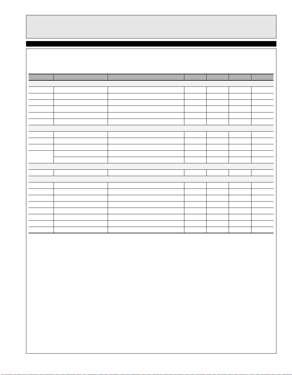
Electrical Characteristics
VS+ = +15V, VS- = 0V, VH = +15V, VL = 0V , TA = 25°C, unless otherwise specified
Parameter Description Condition Min Typ Max Units
Input
V
IH
I
IH
V
IL
I
IL
C
in
R
in
Output
R
OV1
R
OV2
I
leak
I
PK
Power Supply
I
S
Switching Characteristics
t
R
t
F
t
RFdelta
t
D-1
t
D-2
t
Ddelta
T
enable
T
disable
Logic “1” Input Voltage 2.4 V Logic “1” Input Current VIH = 5V 0.1 10 µA Logic “0” Input Voltage 0.8 V Logic “0” Input Current VIL = 0V 0.1 10 µA
Input Capacitance 3.5 pF
Input Resistance 50 MΩ
ON Resistance VH to OUT I ON Resistance VL to OUT I
= -100mA 3.5 5 Ω
OUT
= +100mA 3 5 Ω
OUT
Output Leakage Current VH = VS+, VL = VS-0.110µA
Peak Output Current Source 2.0 A
Sink 2.0 A
Power Supply Current Inputs = VS+0.82mA
Rise Time CL = 1000pF 11 ns
Fall Time CL = 1000pF 12 ns
tR, tF Mismatch CL = 1000pF 1 ns
Turn-Off Delay Time CL = 1000pF 11.5 ns
Turn-On Delay Time CL = 1000pF 13 ns
t
- t
Mismatch CL = 1000pF 1.5 ns
D-1
D-2
Enable Delay Time 12 ns
Disable Delay Time 12 ns
EL7457C
3
Page 4
EL7457C
40MHz Non-Inverting Quad CMOS Driver
EL7457C
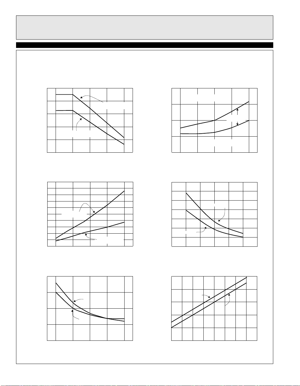
Typical Performance Curves
Max Power
11
1.0
0.8
0.6
0.4
Max Power(W)
0.2
0
Quiescent Supply Current vs Supply Voltage
9
T=25°C
2.0
1.8
1.6
1.4
1.2
1.0
0.8
Supply Current (mA)
0.6
0.4
0.2
0
Rise/Fall Time vs Supply Voltage
1
CL=1000pF, T=25°C
25
θja=158°C/W, QSOP-16
25 10075050
Temperature (°C)
All Inputs = 0
815
5
Supply Voltage (V)
θja=110°C /W , SO - 16
All Inputs = VS+
11
Switch Threshold vs Supply Voltage
10
T=25°C
1.8
High Limit = 2.4V
1.6
VH to OUT
10
Hysteresis
15
1.4
Input voltage (V)
1.2
1.0
“On” Resistance vs Supply Voltage
8
I
=100mA, T=25°C
OUT
9
8
7
6
5
“On” Resistance (Ω)
4
VL to OUT
3
12
2
5
Rise/Fal l Time vs Temperature
2
CL=1000pF, VS+=15V
16
Low Limit = 0.8V
71512510
Supply Voltage (V)
Supply Voltage (V)
20
t
R
15
t
Rise/Fall Time (ns)
10
5
5
F
7.5 15
Supply Voltage (V)
12.5
10
14
12
10
Rise/Fall Time (n s)
8
6
-50
t
F
0
t
R
50
Temperature (°C)
100
150
4
Page 5

Typical Performance Curves (cont.)
EL7457C
EL7457C
40MHz Non-Inverting Quad CMOS Driver
Propagation Delay vs Supply Voltage
3
CL=1000pF, T=25°C
25
20
15
Delay Time (ns)
10
5
5.0
Rise/Fall Time vs Load
5
VS+=15V, T= 25°C
140
120
100
80
60
Rise/Fall Time (ns)
40
20
0
470 10000
100
t
D2
t
D1
7.5 15.0
10.0 12.5
Supply Voltage (V)
t
F
1000 4700
2200
Load Capacitance (pF)
t
R
Propagation ,Delay vs Temperature
4
CL=1000pF, VS+=15V
18
16
t
14
12
Delay Time (ns)
10
8
6
-25 25 75 100
Supply Current Per Channel vs Capacitive Load
6
VS+=VH=10V, VS-=VL=0V, T=25°C, f=100kHz
12
10
8
6
4
Supply Current (mA)
2
0
100 1k 10k
D2
0125-50 50
Temperature (°C)
Load Capacitance (pF)
t
D1
Supply Current Per Channel vs Frequency
7
CL=1000pF, T=25°C
100
10
1.0
Supply Current (mA)
VS+=5V
0.1
VS+=15V
VS+=10V
1M 10M10k 100k
Frequency (Hz)
5
Page 6

EL7457C
40MHz Non-Inverting Quad CMOS Driver
EL7457C
Nominal Operating Voltage Range
PIN MIN MAX
+ to VS- 5V 15V
V
S
V
- to GND -5V 0V
S
VH V
VL V
VH to VL 0V 15V
VL to V
-0V 8V
S
Timing Diagrams
- + 2.5V VS+
S
-V
Input
Output
S
2.5V
0
90%
S
5V
+
10%
t
D1
t
R
t
D2
t
F
6
Page 7

Standard Test Configuration
EL7457C
EL7457C
40MHz Non-Inverting Quad CMOS Driver
10kΩ
INC
IND
VS+
INA
EN
INB
VL
4.7µF
0.1µF
1
2
3
4
5
NC
6
7
8 9
16
15
14
13
NC
12
11
10
1000pF
1000pF
1000pF
1000pF
4.7µF0.1µF
0.1µF
4.7µF
4.7µF0.1µF
VS+
OUTA
OUTB
VH
OUTC
OUTD
VS-
7
Page 8

EL7457C
40MHz Non-Inverting Quad CMOS Driver
EL7457C
Pin Description
Pin Name Function Equivalent Circuit
1 INA Input Channel A
2 OE Output Enable (Reference Circuit 1)
3 INB Input Channel B (Reference Circuit 1)
4 VL Low Voltage Input Pin
5 GND Input Logic Ground
6 NC No Connection
7 INC Input Channel C (Reference Circuit 1)
8 IND Input Channel D (Reference Circuit 1)
9V
10 OUTD Output Channel D
- Negative Supply Voltage
S
VS+
INPUT
VS-
Circuit 1
VH
11 OUTC Output Channel C (Reference Circuit 2)
12 VH High Voltage Input Pin
13 NC No Connection
14 OUTB Output Channel B (Reference Circuit 2)
15 OUTA Output Channel A (Reference Circuit 2)
16 V
+ Positive Supply Voltage
S
8
OUTPUT
VSVL
Circuit 2
Page 9

Block Diagram
EL7457C
EL7457C
40MHz Non-Inverting Quad CMOS Driver
VS+
INPUT
GND
VS-
Level
Shifter
OE
3-State
Control
VH
OUTPUT
VL
9
Page 10

EL7457C
40MHz Non-Inverting Quad CMOS Driver
EL7457C
Application Information:
Product Description
The EL7457 C is a high perfo rmance 40MHz ul tra-h igh
speed quad driver. Each channel of the EL7457C consists of a single P-channel high side driver and a single
N-channel low side driver. These 3Ω devices will pull
the output (OUT
) to either the high or low voltage, on
X
VH and VL respectively, depending on the i nput logic
signal (INX). It should be noted that there is only one set
of high and low voltage pins.
A common output enable (OE) pin is available on the
EL7457C. This pi n, whe n pu lle d low w il l p ut al l ou tp uts
in to the high impedance state.
The EL7457C is available in both the 16-pin SOIC and
the space saving 16- pin QSOP packages. The releva nt
package should be chosen depending on the calculated
power dissipation.
Supply Voltage Range and Input Compatibility
The EL7457C is desi gned fo r ope ration on su pplies f rom
5V to 15V with 10% tolerance (i.e. 4.5V to 16.5V). The
table on page 6 shows the s pe ci fic ations for the relatio nship between the V
+, VS-, VH, VL and GND pins. The
S
EL7457C does not contain a true analog switch and
therefore VL should always be less than VH.
All input pins are compatible with both 3V and 5V
CMOS signals With a positive supply (V
+) of 5V, the
S
EL7457C is also compatible with TTL inputs.
Power Supply Bypassing
When using the EL7457C, it is very important to use
adequate power supp ly bypa ssing. The high switchi ng
currents developed by the EL7457C necessitate the use
of a bypass capacitor on both the positive and negative
supplies. It is recommended that a 4.7µF tantalum
capacitor be used in parallel with a 0.1µF l ow-inductance ceramic MLC capacitor. These should be placed as
close to the supply pins as possible. It is also recommended that the VH and VL pins have some level of
bypassing, especially if the EL7457C is driving highly
capacitive loads.
Power Dissipation Calculation
When switching at high speeds, or driving heavy loads,
the EL7457C drive cap abili ty is limite d by the ri se in d ie
temperature brought abou t by interna l power dissipatio n.
For reliable operation die temperature must be kept
below T
power dissipation f or a given app lic atio n pr io r to selec ting the package type.
Power dissipation ma y be calculated:
where:
• V
S
V
S
• V
out
• C
L
• C
INT
is the quiescent supply current (3mA max.) and
• I
S
• f is frequency
Having obtained the application’s power dissipation, a
maximum package thermal coefficient may be determined, to maintain the internal die temperature below
T
jmax
where:
• T
jmax
• T
max
• PD is the power dissipation calculated above.
Using the value of θ
tion may be selected.
In applications with a θja greater than 158°C/W, a 16-pin
QSOP may be use d. A 1 6- pin SOIC is suitable f o r a p pli cations with a θ
(125°C). It is necessary to calculate the
jmax
4
PD VSIS×()C
+=
∑
1
2
× f×()CLV
INTVS
2
× f×()+
OUT
is the total power supply to the EL7457C (from
+ to VS-),
is the swing on th e output (VH - VL),
is the load capacitance,
is the internal load capacitance (50pF max.),
.
T
–()
ja
jmaxTmax
----------------------------------------=
PD
θ
is the maximum junction t emperature (125°C),
is the maximum operating temperature,
a suitable package for the applica-
ja,
value greater than 110°C/W. However,
ja
10
Page 11

EL7457C
40MHz Non-Inverting Quad CMOS Driver
EL7457C
if the calculated value of θja is less than 110°C/W, the
application must be dera te d to preve nt prematu r e fail u re
of the device, ei ther by reducing the switching fre-
quency, the capacitive load or the maximum operating
temperature.
11
Page 12

EL7457C
40MHz Non-Inverting Quad CMOS Driver
EL7457C
General Disclaimer
Specifications contained in this data sheet are in effect as of the publicat ion date shown. Elantec, Inc. re serves the r ight to make changes in th e circuitry or specifications cont ained herein at a ny time without notice. Elantec , Inc. assumes no res ponsibili ty for t he us e of an y circuits descr ibed
herein and makes no representations that they are free from patent infringement.
WARNING - Life Support Policy
Elantec, Inc. products are not authorized for and should not be used
within Life Support Systems without the specific written consent of
Elantec, Inc. Life Support systems are equipment intend ed to sup-
Élantec, Inc.
675 Trade Zone Blvd.
Milpitas, CA 95035
Telephone: (408) 945-1323
(888) ÉLANTEC
Fax: (408) 945-9305
European Office: +44-118-977-6080
port or sustain life and whose failure to perform when properly used
in accordance with instructions provided can be reasonably
expected to result in significant personal injury or death. Users contemplating applicatio n of Elantec, Inc. P roducts in Li fe Support
Systems are requested to contact Elantec, Inc. factory headquarters
to establish suitable terms & conditions for these applications. Elantec, Inc. ’s warranty is limited to replacement of defective
components and does not cov er injury to persons or prop erty or
other consequential damages.
December 7, 1999
12
Printed in U.S.A.
 Loading...