

Page 1
EL7156C
High Performance Pin Driver
EL7156C
Features
• Clocking Speeds up to 40MHz
• 15ns tr/tf at 2000pF C
LOAD
• 0.5ns Rise and Fall Times
Mismatch
•0.5ns T
ON-TOFF
Prop Delay
Mismatch
• 3.5pF Typical Input Capacitance
• 3.5A Peak Drive
• Low on Resistance of 3.5Ω
• High Capacitive Drive Capability
• Operates from 4.5V t o 18V
Applications
• ATE/Burn-in Testers
• Level Shifting
• IGBT Drivers
• CCD Drivers
Ordering Information
Part No. Package Tape & Reel Outline #
EL7156CN 8-Pin DIP - MDP0031 EL7156CS 8-Pin SOIC - MDP0027 EL7156CS-T7 8-Pin SOIC 7” MDP0027 EL7156CS-T13 8-Pin SOIC 13” MDP0027
General Description
The EL7156C high-performance pin driver with tri-state is suited to
many ATE and level-shifting applications. The 3.5A peak drive capability makes this part an e xcellent choice when driving h igh
capacitance loads.
The output pi n OUT is c onnec ted to inp ut pins VH o r VL re spect ive ly,
depending on the status o f th e IN pi n. W hen t he OE pi n is ac tiv e l ow,
the output is placed in the tri-state mode. The isolation of the output
FETs from the power supplies enables VH and VL to be set independently, enabling level-shifting to be implemented. Related to the
EL7155C, the EL7156C adds a lower supply pin V
- and makes VL
S
an isolated and independent input. This feature adds applicat ions flexibility and improves switching response due to the increased
enhancement of the output FETs.
This pin driver has improved performan ce over existing pin drivers. It
is specifically designed to operate at voltages down to 0V across the
switch elements while maintaining good speed and on-resistance
characteristics.
A vailable in the 8-Pin SOIC and 8-Pin PDIP packages, the EL7156C is
specified for oper ation over the -40°C to +85°C temperature range.
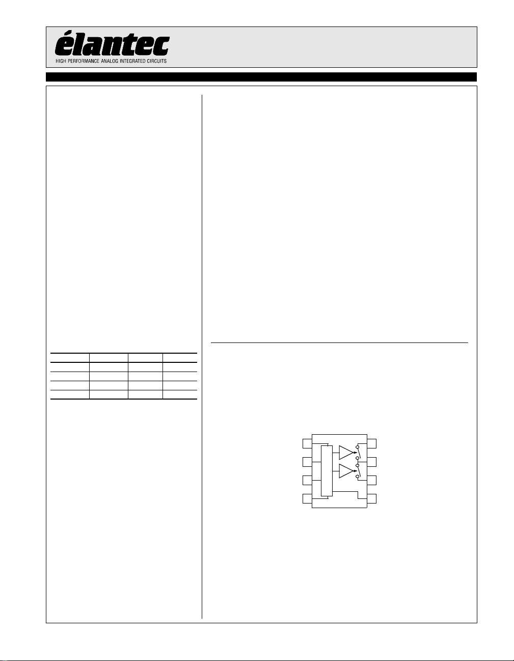
Pin Configuration
© 2000 Elantec Semiconductor, Inc.
VS+
OE
IN
GND
1
L
2
o
g
i
3
c
4
8-Pin PDIP/SOIC
8
VH
7
OUT
6
VL
5
VS-
September 5, 2000
Page 2
EL7156C
High Performance Pin Driver
EL7156C
Absolute Maximum Ratings (T
Absolute maximum ratings are those values beyond which the device
could be permanently damaged. Absolute maximum ratings are stress
ratings only and functional device operation is not implied.
Supply Voltage (V
Input Voltage V
Continuous Output Current 200mA
+ to VS-) +18V
S
= 25°C)
A
- -0.3V, VS +0.3V
S
Storage Temperature Range -65°C to +150°C
Ambient operating Temperature -40°C to +85°C
Operating Junction Temperature 125°C
Power Dissipation see curves
Maximum ESD 2kV
Important Note:
All parameters having Min/Max specifications are guaranteed. Typ values are for information purposes only. Unless otherwise noted, all tests are at the
specified temperature and are pulsed tests, therefore: T
= TC = TA.
J
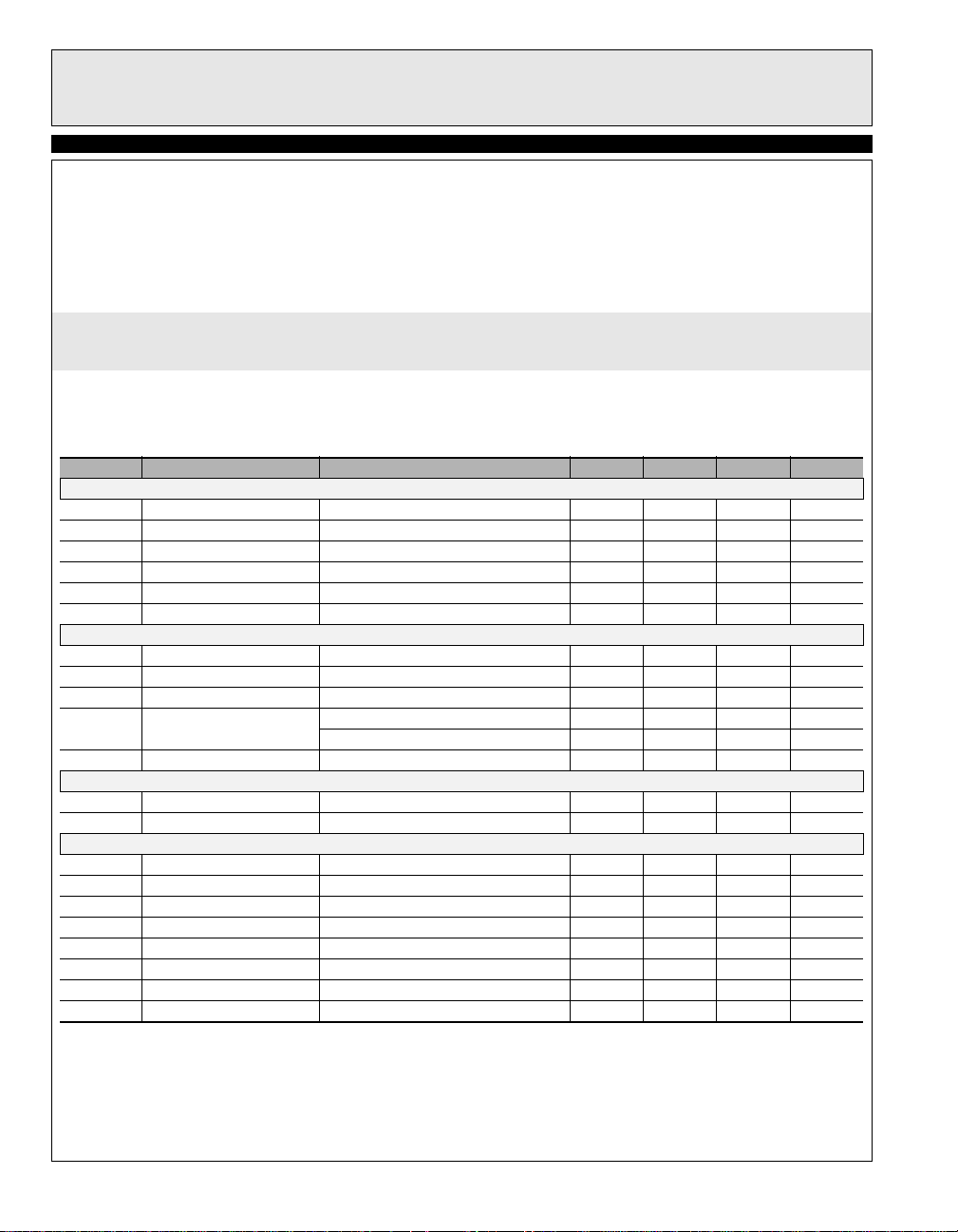
Electrical Characteristics
VS+ = +15V, VH = +15V, VL = 0V, VS-=0V, TA = 25°C, unless otherwise specified
Parameter Description Condition Min Typ Max Units
Input
V
IH
I
IH
V
IL
I
IL
C
IN
R
IN
Output
R
OVH
R
OVL
I
OUT
I
PK
I
DC
Power Supply
I
S
I
VH
Switching Characteristics
t
R
t
F
t
RFdelta
t
D-1
t
D-2
t
Ddelta
t
D-3
t
D-4
Logic ‘1’ Input Voltage 2.4 V Logic ‘1’ Input Current VIH = VS+0.110µA Logic ‘0’ Input Voltage 0.8 V Logic ‘0’ Input Current VIL = 0V 0.1 10 µA
Input Capacitance 3.5 pF
Input Resistance 50 MΩ
ON Resistance VH to OUT I
ON Resistance VL to OUT I
= -200 mA 2.7 4.5 Ω
OUT
= +200 mA 3.5 5.5 Ω
OUT
Output Leakage Current OE = 0V, OUT = VH/VL 0.1 10 µ A
Peak Output Current
(linear resistive operation)
Source 3.5 A
Sink 3.5 A
Continuous Output Current Source/Sink 200 mA
Power Supply Current Inputs = VS+1.33mA
Off Leakage at VH and VL VH, VL = 0V 4 10 µ A
Rise Time CL =2000 pF 14.5 ns
Fall Time CL = 2000 pF 15 ns
tR, tF Mismatch CL = 2000 pF 0.5 ns Turn-Off Delay Time CL = 2000 pF 9.5 ns Turn-On Delay Time CL = 2000 pF 10 ns
t
Mismatch CL = 2000 pF 0.5 ns
D-1-tD-2
Tri-State Delay Enable 10 ns
Tri-State Delay Disable 10 ns
2
Page 3
EL7156C
High Performance Pin Driver
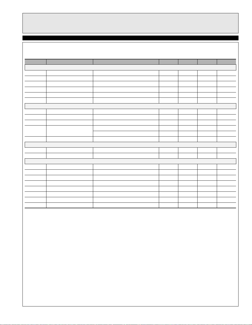
Electrical Characteristics
VS+ = +5V, VH = +5V, VL = -5V, VS- = -5V, TA = 25°C, unless otherwise specified
Parameter Description Condition Min Typ Max Units
Input
V
IH
I
IH
V
IL
I
IL
C
IN
R
IN
Output
R
OVH
R
OVL
I
OUT
I
PK
I
DC
Power Supply
I
S
V
H
Switching Characteristics
t
R
t
F
t
RFdelta
t
D-1
t
D-2
t
Ddelta
t
D-3
t
D-4
Logic ‘1’ Input Voltage 2.0 V Logic ‘1’ Input Current VIH = VS+0.110µA Logic ‘0’ Input Voltage 0.8 V Logic ‘0’ Input Current VIL = 0V 0.1 10 µ A
Input Capacitance 3.5 pF
Input Resistance 50 MΩ
ON Resistance VH to OUT I ON Resistance VL to OUT I
= -200 mA 3.4 5 Ω
OUT
= +200 mA 4 6 Ω
OUT
Output Leakage Current OE = 0V, OUT = VH/VL 0.1 10 µ A
Peak Output Current
(linear resistive operation)
Source 3.5 A
Sink 3.5 A
Continuous Output Current Source/Sink 200 mA
Power Supply Current Inputs = VS+ 1 2.5 mA
Off Leakage at VH and VL VH, VL = 0V 4 10 µ A
Rise Time CL = 2000 pF 17 ns
Fall Time CL = 2000 pF 17 ns
tR, tF Mismatch CL = 2000 pF 0 ns
Turn-Off Delay Time CL = 2000 pF 11.5 ns
Turn-On Delay Time CL = 2000 pF 12 ns
t
Mismatch CL = 2000 pF 0.5 ns
D-1-tD-2
Tri-State Delay Enable 10 ns
Tri-State Delay Disable 10 ns
EL7156C
3
Page 4

EL7156C
High Performance Pin Driver
EL7156C
Typical Performance Curves
Max Power/Derating Curves
1W
8-Lead PDIP
800mW
600mW
8-Lead SO
400mW
Max Power (W)
200mW
Supply Current (mA)
0
2.0
1.6
1.2
0.8
0.4
0
θJA=160°C/W
25 10075050
Quiescent Supply Current vs Supply Voltage
T=25°C
All Inputs = GND
5
θJA=100°C/W
Max TJ=125°C
Temperature (°C)
All Inputs = VS+
10
Supply Voltage (V)
125 150
15
Input Threshold vs Supply Voltage
T=25°C
1.8
1.6
1.4
Input voltage (V)
1.2
1.0
“On” Resistance vs Supply Voltage
I
=200mA, T=25°C, VS+=VH, VS-=VL=0V
OUT
6
5
4
V
OUT
3
2
“On” Resistance (Ω)
1
0
High Threshold
Hysteresis
Low Threshold
Supply Voltage (V)
V
-VL
OUT
-VH
7.5 1512.5510
Supply Voltage (V)
15510
Rise/Fall Time vs Supply Voltage
CL=2000pF, T=25°C
30
25
20
Rise/Fall Time (ns)
15
10
5
t
F
t
R
10
Supply Voltage (V)
Rise/Fall Time vs Temperature
CL=2000pF, VS+=15V
20
18
16
t
I
t
R
15
14
Rise/Fall Time (ns)
12
10
-50
0
t
F
t
R
50
Temperature (°C)
100
150
4
Page 5

Typical Performance Curves
EL7156C
EL7156C
High Performance Pin Driver
Propagation Delay vs Supply Voltage
C
=2000pF, T=25°C
L
17
15
13
Delay Time (ns)
11
9
70
60
50
40
30
Rise/Fall Time (ns)
20
10
0
t
D-1
5
Rise/Fall Time vs Load Capacitance
VS+=+15V, T=25°C
100 1000
t
D-2
10
Supply Voltage (V)
Load Capacitance (pF)
Propagation Delay vs Temperature
C
=2000pF, VS+=15V
L
14
12
10
Delay Time (ns)
8
6
15
t
F
Supply Current (mA)
t
R
10000
-25 25 75 100
Supply Current vs Load Capacitance
+=VH=15V, VS-=VL=0V, T=25°C, f=20kHz
V
S
5
4
3
2
1
0
100 1000 10000
t
D-2
0125-50 50
Temperature (°C)
Load Capacitance (pF)
t
D-1
Supply Current vs Frequency
CL=1000pF, T=25°C
100
10
1.0
Supply Current (mA)
0.1
VS+=15V
VS+=10V
VS+=5V
1M 10M10k 100k
Frequency (Hz)
5
Page 6

EL7156C
High Performance Pin Driver
EL7156C
Truth Table
OE IN OUT
00Tri-state
01Tri-state
10VH
11VL
Timing Diagram
Input
Inverted
Output
0
2.5V
90%
10%
Operating Volta ge Range
PIN MIN MAX
GND - V
--5 0
S
+ - VS-5 18
V
S
VH - VL -18 18
V
+ - VH 0 18
S
+ - GND 5 18
V
S
5V
t
D1
t
F
t
D2
t
R
Standard Test Configuration
VS+
VS+
10k
0.1µ4.7µ
OE
GND
VH
0.1µ 4.7µ
1
L
2
o
g
i
3
IN
c
4
EL7156C
8
7
6
5
2000p
0.1µ 4.7µ
0.1µ 4.7µ
OUT
VL
-
VS-
-
6
Page 7

High Performance Pin Driver
Pin Description
Pin Name Function Equivalent Circuit
1V
2 OE Output Enable
3 IN Input Reference Circuit 1
4 GND Ground
5V
6 VL Lower Output Voltage
7 OUT Output
+ Positive Supply Voltage
S
- Negative Supply Voltage
S
VS+
INPUT
V
S
EL7156C
EL7156C
-
Circuit 1
VH
8 VH High Output Voltage
VS-
VS+
VOUT
VS-
VS-
VL
Circuit 2
7
Page 8

EL7156C
High Performance Pin Driver
EL7156C
Block Diagram
VS+
IN
GND
VS-
Level
Shifter
Application Information
Product Description
The EL7156C i s a high p er forma nce 40 MH z p in d r iver .
It contains two analog sw itches con necting VH an d VL
to OUT. Depending on t he value of the IN pin, one of
the two switches will be closed and the other switch
open. An output enable (OE) is also supplied which
opens both switches simultaneously .
Due to the topology of the EL7156C, both the VH and
VL pins can be connected to any voltage between the
+ and VS- pins.
V
S
The EL7156C is availabl e in both the 8-pin SOIC and
the 8-pin PDIP packages. The relevant package should
be chosen depending on the calculated power
dissipation.
Supply Voltage Range and Input Compatibility
The EL7156C is desi gned fo r ope ration on su pplies f rom
5V to 15V (4.5V to 18V maxim um). T he ta ble on pa ge 6
shows the specifications for the relationship betwe en the
+, VS-, VH, VL and GND pins.
V
S
OE
3-State
Control
VH
OUT
VL
All input pins are compatible with both 3V and 5V
CMOS signals. With a positive supply (V
+) of 5V, the
S
EL7156C is also compatible with TTL inputs.
Power Supply Bypassing
When using the EL7156C, it is very important to use
adequate power supply bypassing . The high switching
currents developed by the EL7156C necessitate the use
of a bypass capacito r bet wee n th e suppl ies ( V
+ & VS-)
S
and GND pins. It is recommended that a 2.2µF tantalum
capacitor be used in parallel with a 0.1µF low-inductance ceramic MLC capacitor. These should be placed as
close to the supply pins as possible. It is also recommended that the VH and VL pins have some level of
bypassing, especially if the EL7156C is driving highly
capacitive loads.
Power Dissipation Calculation
When switching at high speeds, or driving heavy loads,
the EL7156C drive cap abili ty is limite d by the ri se in d ie
temperature brought abou t by interna l power dissipatio n.
For reliable operation die temperature must be kept
below T
(125°C). It is necessary to calculate the
jmax
8
Page 9

EL7156C
High Performance Pin Driver
EL7156C
power dissipation for a given application prior to selecting the package type.
Power dissipation may be calculated:
PD VS( IS) C
( V
INT
2
f) CL( V
S
OUT
2
f)××+××+×=
where:
is the total power supply to the EL7156C (from
• V
S
V
+ to GND),
S
is the swing on the output (VH - VL),
• V
out
• C
is the load capacitance,
L
• C
is the internal load capacitance (50pF max.),
INT
is the quiescent supply current (3mA max.) and
• I
S
• f is frequency
Having obtained the application’s power dissipation, a
maximum package thermal coefficient ma y be determined, to maintain the internal die temperature below
T
:
jmax
T
–
jmaxTmax
--------------------------------=
θ
ja
PD
where:
is the maximum junction t emperature (125°C),
• T
jmax
• T
is the maximum operating temperature,
max
• PD is the power dissipation calculated above,
• θja thermal resistance on junction to ambient.
θ
is 160°C/W for the SO8 package and 100°C/W for
ja
the PDIP8 package when using a standard JEDEC
JESD51-3 single-layer test board. If T
is greater than
jmax
125°C when calculated using the equation ab ove, then
one of the following actions must be taken:
• Reduce θ
the system by designing more heat-sinking
ja
into the PCB (as compared to the standard JEDEC
JESD51-3)
• Use the PDIP8 instead of the SO8 package
• De-rate the application either by reducing the switch-
ing frequency, the capacitive load, or the maximum
operating (ambient) temperature (T
max
)
9
Page 10

EL7156C
High Performance Pin Driver
EL7156C
General Disclaimer
Specifications contained in this data sheet are in effect as of the publicat ion date shown. Elantec, Inc. re serves the r ight to make changes in th e circuitry or specifications cont ained herein at a ny time without notice. Elantec , Inc. assumes no res ponsibili ty for t he us e of an y circuits descr ibed
herein and makes no representations that they are free from patent infringement.
WARNING - Life Support Policy
Elantec, Inc. products are not authorized for and should not be used
within Life Support Systems without the specific written consent of
Elantec, Inc. Life Support systems are equipment intend ed to sup-
Elantec Semiconductor, Inc.
675 Trade Zone Blvd.
Milpitas, CA 95035
Telephone: (408) 945-1323
(888) ELANTEC
Fax: (408) 945-9305
European Office: +44-118-977-6080
Japan Technical Center: +81-45-682 -5820
port or sustain life and whose failure to perform when properly used
in accordance with instructions provided can be reasonably
expected to result in significant personal injury or death. Users contemplating applicatio n of Elantec, Inc. P roducts in Li fe Support
Systems are requested to contact Elantec, Inc. factory headquarters
to establish suitable terms & conditions for these applications. Elantec, Inc. ’s warranty is limited to replacement of defective
components and does not cov er injury to persons or prop erty or
other consequential damages.
September 5, 2000
10
Printed in U.S.A.
 Loading...