

Page 1
EL5144C, EL5146C, EL5244C, EL5246C, EL5444C
100 MHz Single Supply Rail to Rail Amplifier
EL5144C, EL5146C, EL5244C, EL5246C, EL5444C
Features
• Rail to Rail Output Swing
5V
0V
• -3 dB Bandwidth = 10 0 MHz
• Single Supply +5V operation
• Power Down to 2.6 µA
• Large Input Common Mode Range
0V < V
CM
< 3.5 V
• Diff Gain/Phase = 0.1%/0. 1°
• Low Power 35mW per amplifier
• Space Saving SOT23-5, MSOP8&10, & QSOP-16 pac ka g ing
Applications
• Video Amplifier
• 5 Volt Analog Signal Processing
• Multiplexer
• Line Driver
• Portable Computers
• High Speed Comm unications
• Sample & Hold Amplifier
•Comparator
Ordering Information
Part No Temp. Range Package Outline #
EL5144CW -40°C to +85 °C 5 Pin SOT23 MDP0038 EL5146CN -40°C to +85°C 8 Pin PDIP MDP0031 EL5146CS -40°C to +8 5 °C 8 Pin SOIC MDP0027 EL5244CN -40°C to +85°C 8 Pin PDIP MDP0031 EL5244CS -40°C to +8 5 °C 8 Pin SOIC MDP0027 EL5244CY -40°C to +85°C 8 Pin MSOP MDP0043 EL5246CN -40°C to +85°C 14 Pin PDIP MDP0031 EL5246CS -40°C to +8 5 °C 14 Pin SOIC MDP0027 EL5246CY -40°C to +85°C 10 Pin MSOP MDP0043 EL5444CN -40°C to +85°C 14 Pin PDIP MDP0031 EL5444CS -40°C to +8 5 °C 14 Pin SOIC MDP0027 EL5444CU -40°C to +85°C 16 Pin QSOP MDP0040
© 1998 Elantec, Inc.
General Description
The EL5144C series amplifiers are voltage feedbac k, high speed, rail
to rail amplifiers designed to operate on a single +5V supply. They
offer unity gain stability with an unloaded –3dB bandwidth of 100
MHz. The input common mode v oltage range ex tend s from the negative rail to within 1.5V of the positive rail. Driving a 75Ω double
terminated coaxial cable, the EL5144C series amplifiers drive to
within 150 mV of either rail. The 200 V/µsec slew rate and 0.1% / 0.1°
differential gain / differential phase makes these parts ideal for composite and component video applicat ions. With its voltage feedback
architecture, this amplifier can accept reactive feedback networks,
allowing them to be used in analog filtering applications These amplifiers will source 90 mA and sink 65 mA.
The EL5146C and EL5246C have a power-savings disable feature.
Applying a standard TTL low logic level to the CE (Chip Enable) pin
reduces the supply current to 2.6 µA within 10 nsec. Turn on time is
500 nsec, allowing true break-before-make conditions for multiplexing applications. Allowing the CE pin to float or applying a high logic
level will enable the amplifier.
For applications where board space is critical, singles are offered in a
SOT23-5 package, duals in MSOP-8 and MSOP-10 packages, and
quads in a QSOP-16 package. Singl es, duals an d quads are also avail able in industry standard pinouts in SOIC and PDIP packages. All
parts operate over the industrial temperature range of -40°C to +85°C.
Pin Configurations
SOT23-5
OUT
GND
IN+
1
+
2
3
-
EL5144C
V
5
S
IN-
4
GND
Dual and Quad Amplifier Pin Configura tions on Page 12
SOIC-8, PDIP-8
NC
1
IN-
2
-
IN+
+
3
4
EL5146C
CE
8
V
7
S
OUT
6
NC
5
March 1, 2000
Page 2
EL5144C, EL5146C, EL5244C, EL5246C,
EL5444C
100 MHz Single Supply Rail to Rail Amplifier
Absolute Maximum Ratings (T
Values beyond absolute maximum ratings can cause the device to be prematurely damaged. Absolute maximum ratings are stress ratings only and
functional device operation is not implied.
Supply Voltage between V
Maximum Continuous Output Current 50mA
and GND +6V
S
= 25 °C)
A
Power Dissipation See Curves
Pin Voltages GND - 0.5V to V
Storage Temperature -65°C to +150°C
Operating Temperature -40°C to +85°C
Lead Temperature 260°C
Important Note:
All parameters having Min/Max specifications are guaranteed. Typ values are for information purposes only. Unless otherwise noted, all tests are at the specified
temperature and are pulsed tests, therefore: T
= TC = TA.
J
Electrical Characteristics
VS=+5V, GND=0V, TA=25°C, CE = +2V, unless otherwise specified.
Parameter Description Conditions Min Typ Max Units
AC Performance
dG Differential Gain Error
dP Differential Phase Error
EL5144C, EL5146C, EL5244C, EL5246C, EL5444C
BW Bandwidth -3dB, G=1, R
BW1 Bandwidth ±0.1dB, G=1, R
GBWP Gain Bandwidth Product 60 MHz
SR Slew Rate G=1, R
ts Settling Time to 0.1%, V
DC Performance
A
V
T
I
B
VOL
OS
CVOS
Open Loop Voltage Gain RL=no load, V
Offset Voltage VCM=1V, SOT23-5 and MSOP packages 25 mV
Input Offset Voltage Temperature Coefficient 10 µV/OC
Input Bias Current VCM=0V & 3.5V 2 100 nA
Input Characteristics
CMIR Common Mode Input Range CMRR ≥ 47dB 0 3.5 V
CMRR Common Mode Rejection Ratio DC, V
R
IN
C
IN
Input Resistance 1.5 GΩ
Input Capacitance 1.5 pF
Output Characteristics
V
OP
V
ON
+I
OUT
Positive Output V oltage Swing RL=150Ω to 2.5V
Negative Output V oltage Swing RL=150Ω to 2.5V
Positive Output Current RL=10Ω to 2.5V 60 90 120 mA
[1]
[1]
G=2, RL=150Ω to 2.5V, RF=1KΩ 0.1 %
G=2, RL=150Ω to 2.5V, RF=1KΩ 0.1 deg
=10kΩ, RF=0 100 MHz
L
-3dB, G=1, R
3.5V
=150Ω to GND, V
R
L
V
CM
DC, V
R
=150Ω to GND
L
=1KΩ to 2.5V
R
L
R
=150Ω to GND
L
=1K to 2.5V
R
L
=150Ω, RF=0 60 MHz
L
=150Ω to GND, RF=0 8 MHz
L
=150Ω to GND, RF=0, VO=0.5V to
L
= 0 to 3V 35 ns
OUT
=0.5V to 3V 54 65 dB
OUT
=0.5V to 3V 40 50 dB
OUT
150 200 V/µs
=1V, All other packages 15 mV
= 0 to 3.0V 50 60 dB
CM
= 0 to 3.5V 47 60 dB
CM
[2]
[2]
[2]
[2]
[2]
[2]
4.70 4.85 V
4.20 4.65 V
4.95 4.97 V
0.15 0.30 V 0V
0.03 0.05 V
+0.5V
S
2
Page 3
EL5144C, EL5146C, EL5244C, EL5246C,
EL5444C
100 MHz Single Supply Rail to Rail Amplifier
Electrical Characteristics
VS=+5V, GND=0V, TA=25°C, CE = +2V, unless otherwise specified.
Parameter Description Conditions Min Typ Max Units
-I
OUT
Enable (EL5146C & EL5246C Only)
t
EN
t
DIS
I
IHCE
I
ILCE
V
IHCE
V
ILCE
Supply
Is
ON
Is
OFF
PSOR Power Supply Operating Range 4.75 5.0 5.25 V PSRR Power Supply Rejection Ratio DC, V
1. Standard NTSC test, AC signal amplitude = 286 mV
2. R
Negative Output Current RL=10Ω to 2.5V -50 -65 -80 mA
Enable Time EL5146C, EL5246C 500 nS Disable Time EL5146C, EL5246C 10 nS CE pin Input High Current CE = 5V, EL5146C, EL5246C 0.003 1 µA CE pin Input Low Current CE = 0V, EL5146C, EL5246C -1.2 -3 µA CE pin Input High Voltage for Power Up EL5146C, EL5246C 2.0 V CE pin Input Low Voltage for Power Down EL5146C, EL5246C 0.8 V
Supply Current - Enabled (per amplifier) No Load, VIN= 0V, CE=5V 7 8.8 mA
Supply Current - Disabled (per amplifier) No Load, VIN= 0V, CE=0V 2.6 5 µA
= 4.75V to 5.25V 50 60 dB
S
, f=3.58 MHz, VOUT is swept from 0.8V to 3.4V, RL is DC coupled
is Total Load Resistance due to Feedback Resistor and Load Resistor
L
p-p
EL5144C, EL5146C, EL5244C, EL5246C, EL5444C
3
Page 4
EL5144C, EL5146C, EL5244C, EL5246C,
EL5444C
100 MHz Single Supply Rail to Rail Amplifier
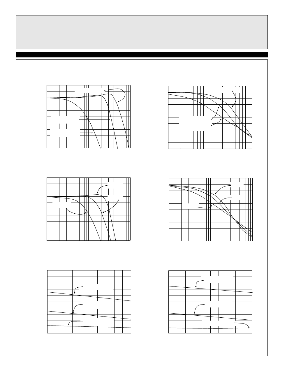
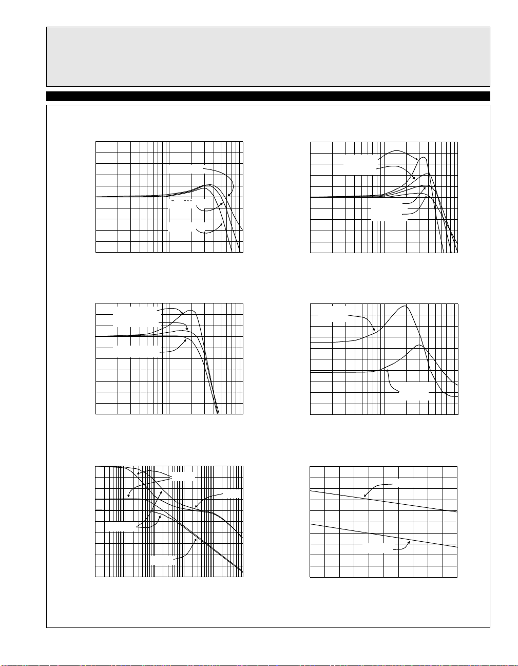
Typical Performance Curves
EL5144C, EL5146C, EL5244C, EL5246C, EL5444C
Non-Inverting Frequency Response (Gain)
19
V
= 1.5V, RL = 150Ω
CM
+2
0
-2
AV = +2, RF = 1KΩ
-4
AV = +5.6, RF = 1KΩ
-6
MAGNITUDE (NORMALIZED) (dB)
-8
1M 10M 100M
Inverting Frequency Response (Gain)
1
= 1.5V, RF = 1KΩ, RL= 150Ω
V
CM
AV = +1, RF = 0Ω
FREQUENCY (Hz)
Non-Inverting Frequency Response (Phase)
15
V
= 1.5V, RL= 150Ω
CM
0
-45
-90
PHASE (°)
-135
-180
1M 10M 100M
2
AV = +2, RF = 1KΩ
AV = +5.6, RF = 1KΩ
FREQUENCY(Hz)
Inverting Frequency Response (Phase)
V
= 1.5V, RF = 1KΩ, RL= 150Ω
CM
AV = +1, RF = 0Ω
+2
0
AV = -5.6
-2
-4
-6
MAGNITUDE (NORMAILZED) (dB)
1M 10M 100M
3dB Bandwidth vs. Die Temperature for Various Gains
52
RL = 150Ω
100
80
60
40
3dB BANDWIDTH (MHz)
20
0
-55 -15 25 65 145105 145
FREQUENCY (Hz)
AV = +1, RF = 0Ω
AV = +2, RF = 1KΩ
AV = +5.6, RF = 1KΩ
DIE TEMPERATU RE (°C)
AV = -1
AV = -2
180
135
90
PHASE (°)
45
0
51
150
120
90
60
3dB BANDWIDTH (MHz)
30
0
-55 -15 25 65 145105 145
AV = -5.6
1M 10M 100M
3dB Bandwidth vs. Die Temperature for Various Gains
RL = 10KΩ
FREQUENCY (Hz)
AV = +1, RF = 0Ω
AV = +2, RF = 1KΩ
AV = +5.6, RF = 1KΩ
DIE TEMPERATURE (°C)
AV = -1
AV = -2
4
Page 5
EL5144C, EL5146C, EL5244C, EL5246C,
EL5444C
100 MHz Single Supply Rail to Rail Amplifier
EL5144C, EL5146C, EL5244C, EL5246C, EL5444C
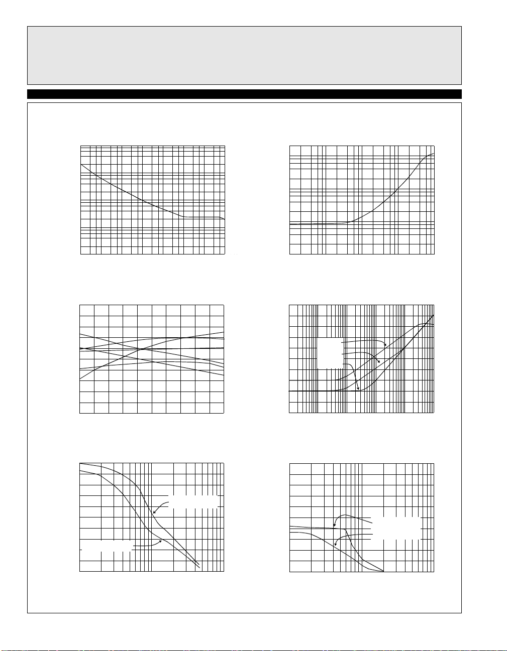
Frequency Response for Various R
16
V
= 1.5V, RF = 0Ω, AV = +1
CM
+4
+2
0
-2
-4
MAGNITUDE (NORMALIZED) (dB)
1M 10M 100M
Frequency Response for Various RF and R
18
V
= 1.5V,RL = 150Ω, AV = +2
CM
+2
0
-2
-4
-6
MAGNITUDE (NORMALIZED) (dB)
1M 10M 100M
Open Loop Gain and Phase vs. Frequency
29
80 RL = 1KΩ
60
40
GAIN (dB)
RL = 150Ω
20
0
1K 100K 10M
FREQUENCY (Hz)
RF = RG = 2KΩ
RF = RG = 1KΩ
RF = RG = 560Ω
FREQUENCY (Hz)
Gain
FREQUENCY (Hz)
L
RL= 10KΩ
RL= 520Ω
RL= 520Ω
RL= 150Ω
Frequency Response for Various C
17
V
= 1.5V, RL = 150Ω, AV = +1
CM
+8
+4
0
-4
-8
MAGNITUDE (NORMALIZED) (dB)
1M 10M 100M
G
0
45
Phase
PHASE (°)
90
135
180
Group Delay vs. Frequency
23
10
8
6
4
GROUP DELAY (nsec)
2
0
1M 10M 100M
Open Loop Voltage Gain vs. Die Temperature
43
80
70
60
50
OPEN LOOP GAIN (dB)
40
30
-55 -15 25 65 145105 145
CL= 100pF
CL= 47pF
AV = +2
RF = 1KΩ
DIE TEMPERATURE (°C)
FREQUENCY (Hz)
FREQUENCY (Hz)
RL=150Ω
CL= 22pF
CL= 0pF
L
AV = +1
RF = 0Ω
No Load
5
Page 6
EL5144C, EL5146C, EL5244C, EL5246C,
EL5444C
100 MHz Single Supply Rail to Rail Amplifier
EL5144C, EL5146C, EL5244C, EL5246C, EL5444C
Voltage Noise vs. Frequency
65
10K
1K
Hz)
√
100
10
VOLTAGE NOISE (nV/
1
10 1K 100K 10M
Offset Voltage vs. Die Temperature
39
(6 Typical Samples)
12
6
0
-6
OFFSET VO LTAGE (mV)
-12
-55 -15 25 65 145105 145
Output Voltage Swing vs. Frequency for THD < 1%
21
RF = 1KΩ, AV = +2
5
FREQUENCY (Hz)
DIE TEMPERATURE ( °C)
Closed Loop Output Impedance vs. Frequency
26
R
= 0, AV = +1
F
200
)
0
20
2
CLOSED LOOP (Z
0.2
10K 100K 1M
PSRR and CMRR vs. Frequency
28
+20
0
-20
-40
PSRR, CMRR (dB)
-60
-80
1K 10K 100K 1M 10M 100M
Output Voltage Swing vs. Frequency for THD < 0.1%
22
RF = 1KΩ, AV = +2
5
FREQUENCY (Hz )
CMRR
-PSRR
+PSRR
FREQUENCY (Hz)
10M
100M
4
3
2
RL = 150Ω to 2.5V
1
OUTPUT VOLTAGE SWING (VPP)
0
1M 10M 100M
FREQUENCY (Hz)
RL = 500Ω to 2.5V
4
3
2
1
OUTPUT VOLTAGE SWING (VPP)
0
1M 10M 100M
FREQUENCY (Hz)
RL = 500Ω to 2.5V
RL = 150Ω to 2.5V
6
Page 7

EL5144C, EL5146C, EL5244C, EL5246C,
EL5444C
100 MHz Single Supply Rail to Rail Amplifier
EL5144C, EL5146C, EL5244C, EL5246C, EL5444C
Large Signal Pulse Response (Single Supply)
62
VS= +5V, RL = 150Ω to 0V, RF = 1KΩ, AV = +2
4
3
2
1
OUTPUT VOLTAGE (V)
0
TIME (20ns/DIV)
Large Signal Pulse Response (Split Supplies)
61
VS= ±2.5V, RL = 150Ω to 0V, RF = 1KΩ, AV = +2
+2
0
-2
OUTPUT VOLTAGE (V)
Small Signal Pulse Response (Single Supply)
63
VS= +5V, RL = 150Ω to 0V, RF = 1KΩ, AV = +2
1.7
1.5
1.3
OUTPUT VOLTAGE (V)
TIME (20ns/DIV)
Small Signal Pulse Response (Split Supply)
64
VS= ±2.5V, RL = 150Ω to 0V, RF = 1KΩ, AV = +2
+0.2
0
-0.2
OUTPUT VOLTAGE (V)
TIME (20ns/DIV)
Settling Time vs. Settling Accuracy
70
RL=1KΩ, RF = 500Ω, AV = -1, V
100
80
60
40
SETTLING TIME (nsec)
20
0
0.01 0.1 1.0
SETTLING ACCURACY (%)
STEP
= 3V
TIME (20ns/DIV)
Slew Rate vs. Die Temperature
48
250
200
SLEW RATE (V/µS)
150
-55 -15 25 65 145105 145
DIE TEMPERATUR E (°C)
7
Page 8

EL5144C, EL5146C, EL5244C, EL5246C,
EL5444C
100 MHz Single Supply Rail to Rail Amplifier
EL5144C, EL5146C, EL5244C, EL5246C, EL5444C
Differential Gain for RL Tied to 0V
54
= 0, AV = +1
R
F
+0.08
+0.04
0
-0.04
DIFFERENTIAL GAIN (%)
-0.08
0.25 1.75
Differential Gain for RL Tied to 2.5V
56
= 0, AV = +1
R
F
+0.2
+0.1
0
-0.1
DIFFERENTIAL GAIN (%)
-0.2
0.5
Differential Gain for RL Tied to 0V
32
RF = 1KΩ, AV = +2
RL = 150Ω
RL = 10KΩ
V
OUT
RL = 150Ω
RL = 10KΩ
2.0
V
OUT
(V)
(V)
3.25
3.5
Differential Phase for R
53
= 0, AV = +1
R
F
+0.2
+0.1
-0.1
DIFFERENTIAL PHASE (°)
-0.2
55
+0.2
+0.2
+0.1
+0.1
-0.1
-0.1
DIFFERENTIAL PHASE (°)
DIFFERENTIAL PHASE (°)
-.02
-.02
34
RL = 150Ω
0
0.25
Differential Phase for RL Tied to 2.5V
Differential Phase for RL Tied to 2.5V
RF = 0, AV = +1
0
0
0.5 2.0
0.5 2.0
Differential Phase for RL Tied to 0V
RF = 1KΩ, AV = +2
Tied to 0V
L
1.75
V
(V)
OUT
RL =
RL = 10KΩ
RL =
RL = 150Ω
V
(V)
V
(V)
OUT
OUT
RL = 10KΩ
3.25
3.5
3.5
+0.2
RL = 150Ω
+0.1
0
-0.1
DIFFERENTIAL GAIN (%)
-0.2
0.5
RL = 10KΩ
2.0
V
(V)
OUT
3.5
+0.2
+0.1
-0.1
DIFFERENTIAL PHASE (°)
-0.2
RL = 150Ω
RL = 10KΩ
0
0.5
2.0
V
(V)
OUT
3.5
8
Page 9

EL5144C, EL5146C, EL5244C, EL5246C,
EL5444C
100 MHz Single Supply Rail to Rail Amplifier
EL5144C, EL5146C, EL5244C, EL5246C, EL5444C
Differential Gain fo r RL Tied to 2.5V
31
R
= 1KΩ, AV = +2
F
+0.2
+0.1
0
-0.1
DIFFERENTIAL GAIN (%)
-0.2
0.5
2nd and 3rd Harmonic Distortion vs. Frequency
5
V
= 0.25V to 2.25V, RL = 100Ω to 0V
OUT
-25
-35
-45
-55
DISTORTION (dBc)
-65
-75
1M 10M 100M
2nd and 3rd Harmonic Distortion vs. Frequency
7
V
= 1V to 3V, RL = 100Ω to 0V
OUT
-25
RL = 150Ω
RL = 10KΩ
2.0
V
(V)
OUT
HD2
FREQUENCY (Hz)
HD3
Differential Phase for RL Tied to 2.5V
33
R
= 1KΩ, AV = +2
F
+0.2
+0.1
0
-0.1
DIFFERENTIAL PHASE (°)
-0.2
3.5
0.5 2.0
2nd and 3rd Harmonic Distortion vs.Frequency
6
V
= 0.5V to 2.5V, RL = 100Ω to 0V
OUT
-25
-35
-45
HD2
-55
DISTORTION (dBc)
-65
-75
1M 10M 100M
Channel to Channel Crosstalk- Duals and Quads
27
(Worst Channel)
0
RL = 10KΩ
RL = 150Ω
V
(V)
OUT
HD3
FREQUENCY (Hz)
3.5
-35
-45
-55
DISTORTION (dBc)
-65
-75
1M 10M 100M
HD3
HD2
FREQUENCY (Hz)
-20
-40
-60
CROSSTALK (dB)
-80
-100
100K 1M 10M 100M
FREQUENCY (Hz)
9
Page 10

EL5144C, EL5146C, EL5244C, EL5246C,
EL5444C
100 MHz Single Supply Rail to Rail Amplifier
EL5144C, EL5146C, EL5244C, EL5246C, EL5444C
Supply Current (per Amp) vs.
44
Supply Voltage
8
6
4
2
SUPPLY CURRENT (mA)
0
012345
SUPPLY VOLTAGE (V)
Supply Current - ON (per amp) vs.
46
Die Temperature
9
8
7
6
SUPPLY CURRENT (mA)
5
4
-55 -15 25 65 145105 145
DIE TEMPERATURE (°C)
Positive Output Voltage Swing vs. Die Temperature
69
RL = 150Ω
5.0
Output Current vs. Die Temperature
45
R
= 10Ω to 2.5V
L
120
100
80
60
OUTPUT CURRENT (mA)
40
20
-55 -15 25 65 145105 145
Supply Current - OFF (per amp) vs.
47
Die Temperature
5
4
3
2
SUPPLY CURRENT (µA)
1
0
-55 -15 25 65 145105 145
Negative Output Voltage Swing vs.
41
Die Temperature
0.5
Source
Sink
DIE TEMPERATURE (°C)
DIE TEMPERATURE (°C)
4.9
4.8
4.7
OUTPUT VOLTAGE (V)
RL=150Ω to 0V
4.6
4.5
-55 -15 25 65 145105 145
DIE TEMPERATUR E (°C)
RL=150Ω to 2.5V
0.4
0.3
0.2
OUTPUT VOLTAGE (V)
0.1
RL=150Ω to 2.5V
RL=150Ω to 0V
0
-55 -15 25 65 145105 145
DIE TEMPERATUR E (°C)
10
Page 11

EL5144C, EL5146C, EL5244C, EL5246C,
EL5444C
100 MHz Single Supply Rail to Rail Amplifier
EL5144C, EL5146C, EL5244C, EL5246C, EL5444C
Output Voltage from Either Rail vs. Die Temperature
40
for Various Effective R
300
100
10
OUTPUT VOLTAGE (mV)
1
-55 -15 25 65 145105 145
67
2.0
1.6
1.2
0.8
0.4
POWER DISSIPATION (W)
0
68
2.5
Effective R
Effective R
Effective R
Maximum Power Dissipation vs. Ambient Temperature
Singles (T
JMAX
SOT23-5, ΘJA = 256°C/W
-50 10 40 70-20
Maximum Power Dissipation vs. Ambient Temperature
Quads (T
JMAX
LOAD
= 150Ω
LOAD
= 1KΩ
LOAD
= 5KΩ
LOAD
Effective R
DIE TEMPERATURE (°C)
= 150°C)
AMBIENT TEMPERAT URE (°C)
= 150°C)
= RL//RF to VS/2
LOAD
PDIP, ΘJA = 110°C/W
SOIC, ΘJA = 161°C/W
100
OFF Isolation - EL5146C & EL5246C
71
-20
-40
EL 5146CS & EL5146CN
-60
-80
MAGNITUDE (dBc)
-100
-120
10k 100k 1M 10M 100M
Maximum Power Dissipation vs. Ambient Temperature
66
Duals (T
2.5
2.0
1.5
1.0
0.5
POWER DISSIPATION (W)
SOIC-8, ΘJA = 159°C/W
MSOP-8,10, ΘJA = 206°C/W
0
-50 10 40 70-20
FREQUE NCY (Hz)
= 150°C)
JMAX
AMBIENT TEMPERATURE (°C)
EL5246CN
EL5246CS
PDIP-14, ΘJA = 87°C/W
PDIP-8, ΘJA = 107°C/W
SOIC-14, ΘJA = 120°C/W
100
2.0
1.5
1.0
0.5
POWER DISSIPATION (W)
SOIC-14, ΘJA = 118°C/W
QSOP-16, ΘJA = 158°C/W
0
-50 10 40 70-20
PDIP-14, ΘJA = 83°C/W
100
AMBIENT TEMP ER ATURE (°C)
11
Page 12

EL5144C, EL5146C, EL5244C, EL5246C,
EL5444C
100 MHz Single Supply Rail to Rail Amplifier
Pin Configurations
SOIC-14, PDIP-14
1
INA+
CEA
GND
CEB
IN
2
NC
3
4
5
6
NC
7
+
B
OUT
EL5144C, EL5146C, EL5244C, EL5246C, EL5444C
SOIC-8, PDIP-8, MSOP- 8
1
A
INA-
2
INA+
3
4
GND
-
+
EL5244C
MSOP-10
1
8
V
S
7
OUT
B
INB-
6
-
INB+
+
5
INA+
CEA
GND
CEB
INB+
-
2
+
3
+
4
-
EL5246C
INA-
10
9
OUT
A
8
V
S
7
OUT
B
65
INB-
-
+
+
-
EL5246C
14
INA-
13
OUT
A
12
NC
11
V
S
10
NC
9
OUT
B
8
INB-
OUT
INA+
INB+
OUT
INA-
V
INB-
1
A
2
3
4
S
5
6
7
B
SOIC-14, PDIP-14
+
-
+
+
-
+
EL5444C
14
OUT
D
-
13
IND-
12
IND+
11
GND
10
INC+
-
9
INC-
8
OUT
C
OUT
INA-
INA+
INB+
INB-
OUT
Single Amplifier Pin Configurations on Page 1
12
QSOP-16
1
A
2
-
+
3
4
V
S
5
V
S
6
+
-
7
8 9
B
EL5444C
16
OUT
D
+
-
15
IND-
14
IND+
13
GND
12
GND
11
INC+
-
+
10
INC-
OUT
C
Page 13

Pin Description
EL5144C, EL5146C, EL5244C, EL5246C, EL5444C
EL5144C, EL5146C, EL5244C, EL5246C,
EL5444C
100 MHz Single Supply Rail to Rail Amplifier
EL5444C
(SO/PDIP)
(QSOP)
Name Function Equivalent Circuit
Positive Power Supply
S
V
S
GND
Circuit 1
V
S
GND
Circuit 2
+ Amplifier A Noninverting Input (Reference Circuit 1)
A
- Amplifier A Inverting Input (Reference Circuit 1)
A
Amplifier A Output (Reference Circuit 2)
A
+ Amplifier B Noninverting Input (Reference Circuit 1)
B
- Amplifier B Inverting Input (Reference Circuit 1)
B
Amplifier B Output (Reference Circuit 2)
B
+ Amplifier C Noninverting Input (Reference Circuit 1)
C
- Amplifier C Inverting Input (Reference Circuit 1)
C
Amplifier C Output (Reference Circuit 2)
C
+ Amplifier D Noninverting Input (Reference Circuit 1)
D
- Amplifier D Inverting Input (Reference Circuit 1)
D
Amplifier D Output (Reference Circuit 2)
D
(SO/PDIP/MSOP)
(MSOP)
EL5246C
EL5246C
EL5444C
(SO/PDIP)
10 11 IN
910IN
8 9 OUT
12 14 IN
13 15 IN
14 16 OUT
EL5144C
EL5146C
(SOT23-5)
57881144,5V
244341112,13GNDGround or Negative Power Supply
3 3 IN+ Noninverting Input
4 2 IN- Inverting Input (Reference Circuit 1)
1 6 OUT Amplifier Output
EL5244C
(SO/PDIP)
31133IN
210142 2IN
191311OUT
55756IN
66867IN
77978OUT
13
Page 14

EL5144C, EL5146C, EL5244C, EL5246C,
EL5444C
100 MHz Single Supply Rail to Rail Amplifier
Pin Description
EL5144C
EL5144C, EL5146C, EL5244C, EL5246C, EL5444C
EL5146C
(SOT23-5)
EL5244C
(SO/PDIP)
8 CE Enable (Enabled when high)
1,5 2,6,
(MSOP)
EL5246C
EL5246C
EL5444C
(SO/PDIP/MSOP)
2 3 CEA Enable Amplifier A (Enabled when high) (Reference Circuit 3)
4 5 CEB Enable Amplifier B (Enabled when high) (Reference Circuit 3)
(SO/PDIP)
10,12
EL5444C
(SO/PDIP)
(QSOP)
Name Function Equivalent Circuit
NC No Connect. Not internally connected.
GND
V
S
Circuit 3
+
1.4V
–
14
Page 15

EL5144C, EL5146C, EL5244C, EL5246C,
100 MHz Single Supply Rail to Rail Amplifier
Description of Operation and Applications Information
EL5144C, EL5146C, EL5244C, EL5246C, EL5444C
EL5444C
Product Description
The EL5144C series is a family of wide bandwidth, single supply, low power, rail-to-rail output, voltage
feedback operational amplifiers. The family includes
single, dual, and qu ad configurati ons. The singles and
duals are available with a power down p in to reduce
power to 2.6µA typically. All the amplifiers are internally compensated for closed loop feedbac k gains of +1
or greater. Larger gains are acceptable but bandwidth
will be reduced according to the familiar Gain-Bandwidth Product.
Connected in voltage follower mode and driving a high
impedance load, the EL5144C series ha s a -3dB bandwidth of 100 MHz. Driving a 150Ω load, they have a
-3dB bandwidth of 60 MHz while main taining a 200
V/µS slew rate. The input common mode voltage range
includes ground while the output can swing rail to rail.
Power Supply Bypassing and Printed Circuit
Board Layout
As with any high-frequency device, good printed circuit
board layout is necessary for optimum performance.
Ground plane constructio n is highly recommended.
Lead lengths should be as short as possible. The power
supply pin must be well bypassed to reduce the risk of
oscillation For normal single supply operation, where
the GND pin is connected to the ground plane, a single
4.7 µF tantalum capacitor in parallel with a 0.1 µF
ceramic capacitor from V
same capacitor combination should be placed at each
supply pin to ground if split supplies are to be used. In
this case, the GND pin becomes the negative supply rail.
For good AC performance, parasitic capacitance should
be kept to a minimum. Use of wire wound resistors
should be avoided because of their additional series
inductance. Use of sockets, particularly for the SO package, should be avoided if possible. Sockets add parasitic
inductance and capacitance that can result in compromised performance.
to GND will suffice. This
S
Input, Output, and Supply Vo ltage Range
The EL5144C series has been designed to operate with a
single supply voltage of 5V. Split supplies can be used
so long as their total range is 5V.
The amplifiers have an input common mode voltage
range that includes the negative supply (GND pin) and
extends to within 1.5V of the positive supply (V
They are specified over this range.
The output of the EL5144C series amplifiers can swing
rail to rail. As the load resistance becomes lower in
value, the ability to drive close to each rail is reduced.
However, even with an effective 150 Ω load resistor
connected to a voltage h a lfway b e tween th e sup pl y rails,
the output will swing to within 150mV of either rail.
pin).
S
15
Page 16

EL5144C, EL5146C, EL5244C, EL5246C,
EL5444C
100 MHz Single Supply Rail to Rail Amplifier
Figure 1 shows the ou tpu t of the EL 51 44C se rie s amp lifier swinging rail to rail with R
= 1KΩ, AV = +2 and R
F
= 1MΩ. Figure 2 is with RL = 150 Ω.
5V
0V
Figure 1
EL5144C, EL5146C, EL5244C, EL5246C, EL5444C
5V
0V
Figure 2
Choice of Feedback Resistor, R
These amplifiers are optimized for applications that
require a gain of +1. Hence, no feedback resistor is
required. However, for gains greater than +1, the feedback resistor forms a pole with the input capacitance. As
this pole becomes larger, phase margin is reduced. This
causes ringing in the time d omain and peakin g in the frequency domain. Therefore, R
value that should not be exceeded for optimum performance. If a large value of R
capacitor in the few picofarad range in parallel with R
can help to reduce this ringing and peaki ng at the
expense of reducing the bandwidth.
As far as the output stage of the amplifier is concerned,
+ RG appear in parallel with RL for gains other than
R
F
F
has some maximum
F
must be used, a small
F
+1. As this combination gets smaller, the bandwidth
falls off. Consequently, R
L
also has a minimum value
F
that should not be exceeded for optimum performance.
= +1, RF = 0 Ω is optimum. For AV = -1 or +2
For A
V
(noise gain of 2), optimum response is obtained with R
between 300 Ω and 1K Ω. For AV = -4 or +5 (noise gain
of 5), keep R
between 300 Ω and 15K Ω.
F
Video Performance
For good video signal integrity, an amplifier is required
to maintain the same output im pedance an d the same frequency response as DC levels are changed at the output.
This can be difficult when driving a standard video load
of 150Ω, because of th e change in outp ut current with
DC level. A look at the Differential Gain and Differential Phase curves for various su pply and loading
conditions will help you obtain optimal performance.
Curves are provided for A
= +1 and +2, and RL = 150Ω
V
and 10 KΩ tied both t o gr ound as wel l as 2.5V. As wit h
all video amplifiers, there is a common mode swe et spot
for optimum differential gain / differential phase. For
example, with A
= +2 and RL = 150Ω tied to 2.5V, an d
V
the output common mode voltage kept between 0.8V
and 3.2V, dG/dP is a very low 0.1% / 0.1°. This condition corresponds to driving an AC-coupled, double
terminated 75Ω c oaxial c able. Wi th AV = +1, RL =
150Ω tied to ground, and the video level kept between
0.85V and 2.95V, these ampl ifiers pro vide dG/dP pe rformance of 0.05% / 0.20°. This cond ition is
representative of using the EL5144 C series amplifier as
a buffer driving a DC coupled, double terminated, 75Ω
coaxial cable. Driving high impedance loads, such as
signals on computer video cards, gives similar or better
dG/dP performance as driving cabl es.
Driving Cables and Capacitive Loads
The EL5144C series amplifiers can drive 50pF loads in
parallel with 150 Ω with 4dB of pe akin g an d 100 pF with
7dB of peaking. If less p eaking is desired in these applications, a small series resistor (usually between 5 Ω and
F
50 Ω) can be placed in series with the outpu t to eliminate
most peaking. However, this will obviously reduce the
gain slightly. If your gain is greater than 1, the gain
resistor (R
) can then be c hosen to make u p f o r a n y ga in
G
F
16
Page 17

EL5144C, EL5146C, EL5244C, EL5246C,
EL5444C
100 MHz Single Supply Rail to Rail Amplifier
EL5144C, EL5146C, EL5244C, EL5246C, EL5444C
loss which may be created by this additional resistor at
the output. Another method of reducing peaking is to
add a “snubber” circuit at the output. A snubber is a
resistor in a series with a capacitor, 150Ω and 100pF
being typical values. The advantage of a snubber is that
it does not draw DC load current.
When used as a cable driver, double termination is
always recommended for reflection-free performance.
For those applications, the back-termination series resistor will de-couple the EL5144C series amp lifier from the
cable and allow extensive capacitive drive. Howe ver,
other applications may have high capacitive loads without a back-termination resistor. Again, a small series
resistor at the output can reduce peaking.
Disable / Power-Down
The EL5146C and EL5246C amplifiers can be disabled,
placing its output in a high-impedance state. Turn off
time is only 10 nsec and turn on time is around 500 nsec.
When disabl ed , th e amp lif i er’s supply current is reduced
to 2.6µA typically, thereby effectively eliminating
power consump tio n. The amplifier’s power down can be
controlled by standard TTL or CMOS signal levels at the
CE pin. The applied logic signal is relative to the GND
pin. Letting the CE pin float will enable the amplifier.
Hence, the 8 pin PDIP and SOIC single amps are pin
compatible with standard amplifiers that don’t have a
power down feature.
Short Circuit Current Limit
The EL5144C series amplifiers do not have internal
short circuit protection circuitry. Short circuit current of
90 mA sourcing a nd 65 mA sin king typi cally will flow if
the output is trying to drive high or low but is shorted to
half way between the rails. If an output is shorted indefinitely, the power dissipatio n could easily increase such
that the part will be destroyed. Maximum reliability is
maintained if the output current never exceeds ±50mA.
This limit is set by internal metal interconnect limitations. Obviously, short circuit conditions must not
remain or the internal metal connections will be
destroyed.
Power Dissipation
With the high output drive capability of the EL5144C
series amplifiers, it is possible to exceed the 150°C
Absolute Maximum junction temperature under certain
load current conditions. Therefore, it is important to calculate the maximum junction temperature for the
application to determine if load conditions or package
type need to be modified for the amplifier to remain in
the safe operating area.
The maximum power dissipation allowed in a package is
determined according to:
T
–
PD
MAX
where:
JMAX = Maximum Junction Temperature
T
AMAX = Maximum Ambient Temperature
T
JA = Thermal Resistance of the Package
θ
MAX = Maximum Power Dissipation
PD
in the Package.
The maximum power dissipation actually pr oduced by
an IC is the total quiescent supply current times the total
power supply voltage, plus the power in the IC due to the
load, or:
PD
MAX
NVSI
=
•
where:
N = Number of amplifiers in the packag e
= Total Supply Voltage
V
S
JMAXTAMAX
----------------------------------------------=
Θ
JA
SMAXV(SVOUT
V
OUT
)
--------------- -•–+•
R
L
17
Page 18

EL5144C, EL5146C, EL5244C, EL5246C,
EL5444C
100 MHz Single Supply Rail to Rail Amplifier
I
= Maximum Supply Current Per Amplifier
SMAX
= Maximum Output Voltage of the Ap plication
V
OUT
= Load Resistance tied to Ground
R
L
If we set the two PD
we can solve for R
equations equal to each other,
MAX
:
L
ure 4 is a graph of propagation delay vs. overdrive as a
square wave is presented at the input of the comparator.
1
EL5146C
2
+2.5V
+
V
IN
–
-
+
3
4
8
7
6
5
+5V
0.1µF
V
OUT
R
L
V
R
----------------------------------------------------------------------------------------------=
L
OUTVSVOUT
T
–
JMAXTAMAX
----------------------------------------------
Θ•
N
JA
VSI
•()–
)–(•
SMAX
EL5144C, EL5146C, EL5244C, EL5246C, EL5444C
Assuming worst case conditions of TA = +85°C, Vout =
/2 V, VS = 5.5V, and I
V
S
below is a table of all packages and the minimum R
allowed.
Part Package Minimum R
EL5144CW
EL5146CS SOIC-8
EL5146CN PDIP-8 14
EL5244CS SOIC-8 48 EL5244CN PDIP-8 30 EL5244CY MSOP-8 69 EL5246CY MSOP-10 69
EL5246CS SOIC-14 34 EL5246CN PDIP-14 23 EL5444CU
EL5444CS SOIC-14 85 EL5444CN PDIP-14 51
SOT23-5 37
QSOP-16
EL5144C Series Comparator Application
The EL5144C series amplifier can be used as a very fast,
single supply comparator. Most op amps used as a comparator allow only slow speed operation because of
output saturation issues. The EL5144C series amplifier
doesn’t suffer from output saturation issues. Figure 3
shows the amplifier implemented as a comparator. Fig-
= 8.8mA per amplifier,
SMAX
L
21
139
Figure 3
Propagation Delay vs. Overdrive for Amplifier Used as a
8
Comparator
1000
L
100
PROPAGATION DELAY(nsec)
10
0.01 0.1 1.0
Positive Going Signal
Negative Going Signal
OVERDRIVE (V)
Figure 4
Multiplexing with the EL5144C Series
Amplifier
Besides normal power down usage, the CE (Chip
Enable) pin on the EL5146C and EL5246C series amplifiers also allow for multiplexing applications. Figure 5
shows an EL5246C with its outputs tied together, driving a back terminated 75Ω video load. A 3 Vp-p 10 MHz
sine wave is applied at Amp A input, and a 2.4 Vp-p 5
MHz square wave to Amp B. Figure 6 shows the
SELECT signal that is applied, and the resulting output
waveform at V
operation of the multiplexing. Amp A is on and V
being passed through to the output of the amplifier. Then
Amp A turns off in about 10 nsec. The output decays to
. Observe the break-before-make
OUT
IN1
is
18
Page 19

EL5144C, EL5146C, EL5244C, EL5246C,
EL5444C
100 MHz Single Supply Rail to Rail Amplifier
EL5144C, EL5146C, EL5244C, EL5246C, EL5444C
ground with an RLCL time consta nts. 500 nsec later,
Amp B turns on and V
is passed through to the out-
IN2
put. This break-before-make operation ensures that more
than one amplifier isn’t trying to drive the bus at the
same time. Notice the outputs are tied directly together.
Isolation resistors at each output are not necessary.
V
1
IN
3V
Select
V
OUT
10MHz
V
2.4V
5MHz
5V
1
PP
-
2
+
3
EL5246C
4
5
+
6
2
IN
PP
-
7
Figure 5
14
V
13
12
11
10
9
8
OUT
+5V
0.1µF4.7µF
150Ω
Free Running Oscillator Application
Figure 7 is an EL5144C configured as a free running
oscillator. To first order, R
frequency of oscillation acc ording to:
F
OSC
For rail to rail output swings, maximum frequency of
oscillation is around 15 MHz. If reduced output swings
are acceptable, 25 MHz can be achieved. Figure 8 shows
the oscillator for R
= 6 MHz.
F
OSC
470K
470K
OSC
470K
1
+
2
3
and C
OSC
0.72
------------------------------------=
C•
R
OSC
OSC
= 510 Ω, C
5
-
0.1µF
4
determine the
OSC
= 240 pF and
OSC
+5V
R
OSC
C
OSC
Select
0V
5V
0V
5V
Figure 6
V
OUT
0V
19
Figure 7
Figure 8
Page 20

EL5144C, EL5146C, EL5244C, EL5246C,
EL5444C
100 MHz Single Supply Rail to Rail Amplifier
EL5144C, EL5146C, EL5244C, EL5246C, EL5444C
General Disclaimer
Specifications contained in this data sheet are in effect as of the publicat ion date shown. Elantec, Inc. re serves the r ight to make changes in th e circuitry or specifications cont ained herein at a ny time without notice. Elante c, Inc. assumes no res ponsibili ty for t he us e of any circuits described
herein and makes no representations that they are free from patent infringement.
WARNING - Life Support Policy
Elantec, Inc. products are not authorized for and should not be used
Elantec Semiconductor, Inc.
675 Trade Zone Blvd.
Milpitas, CA 95035
Telephone: (408) 945-1323
Fax: (408) 945-9305
Toll Free: 1 - (888) ELANTEC
Web Site: http://www.elantec.com
European Office: 44-118-977-6020
Japan Tech Center: 81 -45-682-5820
within Life Support Systems without the specific written consent of
Elantec, Inc. Life Support systems are equipment intend ed to support or sustain life and whose failure to perform when properly used
in accordance with instructions provided can be reasonably
expected to result in significant personal injury or death. Users contemplating applicatio n of Elantec, In c. Products in Li fe Support
Systems are requested to contact Elantec, Inc. factory headquarters
to establish suitable terms & conditions for these applications. Elantec, Inc. ’s warranty is limited to replacement of defective
components and does not cov er injury to per sons or prop erty or
other consequential damages.
March 1, 2000
20
Printed in U.S.A.
 Loading...