

Page 1
EL5283C - Preliminary
Dual and Window 8ns High-Speed Comparators
EL5283C - Preliminary
Features
• 8ns typ. propagation delay
• 5V to 12V input supply
• +2.7V to +5V output supply
• True-to-ground input
• Rail-to-rail outputs
• Active low latch
• Single available (EL5181C)
• Quad available (EL5481C &
EL5482C)
• Pin-compatible 4ns family
available (EL5x85C, EL5287C &
EL5486C)
Applications
• Threshold detection
• High speed sampling circuits
• High speed triggers
• Line receivers
• PWM circuits
• High speed V/F converters
Ordering Information
Part No. Package Tape & Reel Outline #
EL5283CY 10-Pin MSOP - MDP0043
EL5283CY-T13 10-Pin MSOP 13” MDP0043
General Description
The EL5283C comparator is designed for operation in single supply
and dual supply applications with 5V to 12V between VS+ and VS-.
For single supplies, the inputs can operate from 0.1V below ground for
use in ground-sensing applications.
The output side of the comparators can be supplied from a single supply of 2.7V to 5V. The rail-to-rail output swing enables direct
connection of the comparator to both CMOS and TTL logic circuits.
The latch input of the EL5283C can be used to hold the comparator
output value by applying a low logic level to the pin.
The EL5283C contains two comparators set up as a window comparator. A single input is compared with a high and low reference. When
the output goes beyond one of these reference signals, the relevant output goes high.
The EL5283C in the 10-pin MSOP package and is specified for operation over the full -40°C to +85°C temperature range. Also available
are a single (EL5181C) and quad versions (EL5481C and EL5482C).
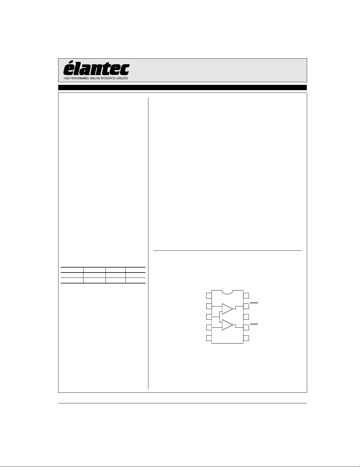
Pin Configurations
1
VS+
2
VREFH
IN
VREFL
VS-
Note: All information contained in this data sheet has been carefully checked and is believed to be accurate as of the date of publication; however, this data sheet cannot be a “controlled document”. Current revisions, if any, to these
specifications are maintained at the factory and are available upon your request. We recommend checking the revision level before finalization of your design documentation.
© 2001 Elantec Semiconductor, Inc.
+
-
3
+
4
-
5 6
EL5283C
(10-Pin MSOP)
10
VSD
9
OUTH
8
LATCH
7
OUTL
GND
September 6, 2001
Page 2
EL5283C - Preliminary
Dual and Window 8ns High-Speed Comparators
Absolute Maximum Ratings (T
Absolute maximum ratings are those values beyond which the device
could be permanently damaged. Absolute maximum ratings are stress
ratings only and functional device operation is not implied.
Analog Supply Voltage (VS+ to VS-) +13.2V
EL5283C - Preliminary
Digital Supply Voltage (VSD to GND) +7V
Differential Input Voltage [(VS-) -0.2V] to [(VS+) +0.2V]
Important Note:
All parameters having Min/Max specifications are guaranteed. Typ values are for information purposes only. Unless otherwise noted, all tests are at the
specified temperature and are pulsed tests, therefore: TJ = TC = TA.
= 25°C)
A
Common-mode Input Voltage [(VS-) -0.2V] to [(VS+) +0.2V]
Latch Input Voltage -0.2V to [(VSD) +0.2V]
Storage Temperature Range -65°C to +150°C
Ambient Operating Temperature -40°C to +85°C
Operating Junction Temperature 125°C
Power Dissipation See Curves
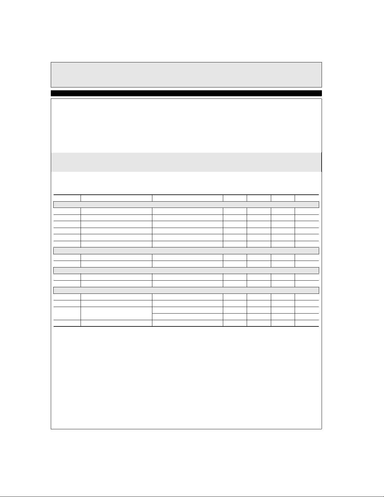
Electrical Characteristics
VS = ±5V, VSD = 5V, R
Parameter Description Condition Min Typ Max Unit
Input
V
OS
I
B
C
IN
I
OS
V
CM
CMRR Common-mode Rejection Ratio -5.1V < V
Output
V
OH
V
OL
Dynamic Performance
tpd+ Positive Going Delay Time VIN = 1V
tpd- Negative Going Delay Time VIN = 1V
Supply
IS+ Positive Analog Supply Current (per comparator) 7 8.2 mA
IS- Negative Analog Supply Current (per comparator) 5 6.5 mA
I
SD
PSRR Power Supply Rejection Ratio 60 80 dB
= 2.3kΩ, C
L
Input Offset Voltage V
Input Bias Current -6 -3.5 µA
Input Capacitance 5 pF
Input Offset Current V
Input Voltage Range (VS-) - 0.1 (VS+) - 2.25 V
Output High Voltage V
Output Low Voltage V
Digital Supply Current (per comparator) All inputs high 4 5 mA
= 15pF, TA = 25°C, unless otherwise specified.
L
= 0V, VO = 2.5V 1 4 mV
CM
= 0V, VO = 2.5V -2.5 0.5 2.5 µA
CM
< +2.75V 65 90 dB
CM
> 250mV VSD - 0.6 VSD - 0.4 V
IN
> 250mV GND + 0.25 GND + 0.5 V
IN
, VOD = 50mV 8 12 ns
P-P
, VOD = 50mV 8 12 ns
P-P
(per comparator) All inputs low 0.75 1 mA
2
Page 3
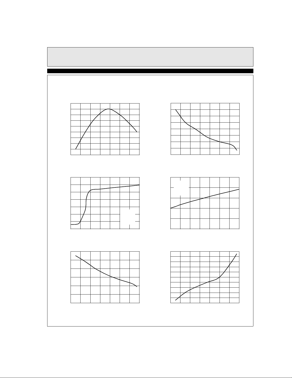
Typical Performance Curves
EL5283C - Preliminary
EL5283C - Preliminary
Dual and Window 8ns High-Speed Comparators
Positive Supply Current vs Temperature
(per comparator)
6.15
6.1
6.05
6
5.95
+ (mA)
5.9
S
I
5.85
5.8
5.75
5.7
-50 -30 -10 10 30 50 70 90
Temperature (°C)
Positive Supply Current vs Supply Voltage
(per comparator)
7
6
5
4
+ (mA)
3
S
I
2
1
0
0 71 2 3 4 5 6
VS+ (V)
Input Bias Current vs Temperature
6
5
4
3
IB (µA)
2
1
0
-50 -30 -10 10 30 50 70 90
Temperature (°C)
VS=±5V
VSD=5V
VIN=50mV
TA=25°C
Negative Supply Current vs Temperature
(per comparator)
-4.4
-4.5
-4.6
-4.7
-4.8
- (mA)
S
I
-4.9
-5
-5.1
-5.2
-50 -30 -10 10 30 50 70 90
Temperature (°C)
Negative Supply Current vs Negative Supply Voltage
(per comparator)
5.5
VS=±5V
VSD=5V
5
VIN=50mV
TA=25°C
4.5
- (mA)
S
I
4
3.5
3
0 71 2 3 4 5 6
VS- (V)
Offset Voltage vs Temperature
0.7
0.6
0.5
0.4
0.3
0.2
(mV)
OS
V
0.1
0
-0.1
-0.2
-0.3
-50 -30 -10 10 30 50 70 90
Temperature (°C)
3
Page 4
EL5283C - Preliminary
Dual and Window 8ns High-Speed Comparators
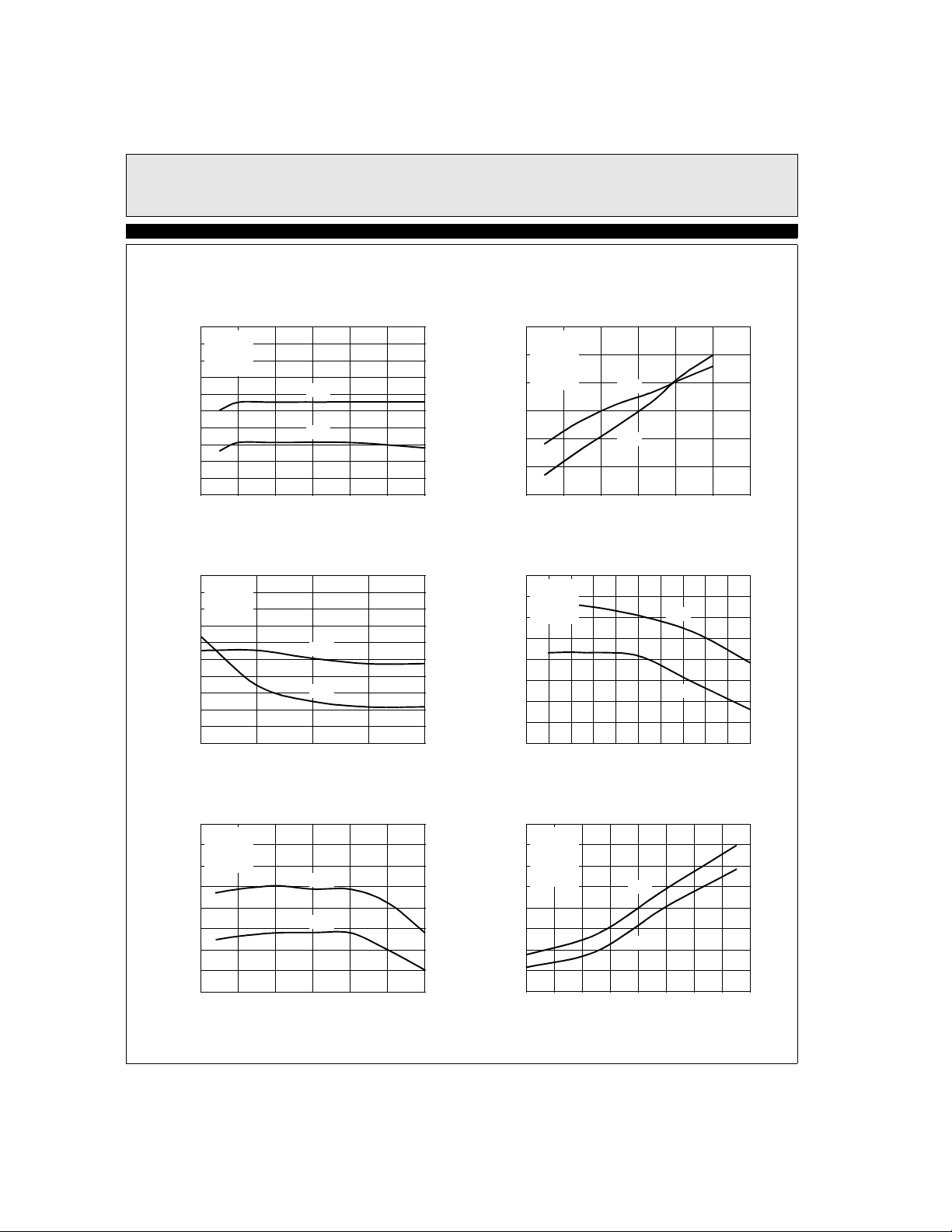
Typical Performance Curves
Propagation Delay vs Overdrive
VIN=1V Step
10
EL5283C - Preliminary
VS=±5V
9.5
VSD=5V
VIN=1V Step
9
RL=2.2kΩ
8.5
8
7.5
7
Delay Time (ns)
6.5
6
5.5
5
0 100 200 300 400 500 600
Propagation Delay vs Supply Voltage
VIN=1V Step
10
VSD=VS+
9.5
VIN=1V Step
VOD=50mV
9
RL=2.2kΩ
8.5
8
7.5
7
Delay Time (ns)
6.5
6
5.5
5
4 4.5 5 5.5 6
Tpd+
Tpd-
VOD (mV)
Tpd+
Tpd-
±VS (V)
Propagation Delay vs Load Capacitance
VIN=1V Step
12
VS=±5V
VSD=5V
11
RL=2.2kΩ
VIN=1V Step
VOD=50mV
10
9
8
Delay Time (ns)
7
6
0 20 40 60 80 100 120
Propagation Delay vs Overdrive
VIN=3V
Step
P-P
10
VS=±5V
9.5
VSD=5V
VIN=1V Step
9
RL=2.2kΩ
8.5
8
7.5
Delay Time (ns)
7
6.5
6
0 0.2 0.6 1 1.2 1.6 2
0.4 0.8 1.4 1.8
Tpd+
Tpd-
C
LOAD
VOD (mV)
(pF)
Tpd+
Tpd-
Propagation Delay vs Overdrive
VIN=5V
Step
P-P
11
VS=±5V
10.5
VSD=5V
RL=2.2kΩ
10
VIN=5V Step
9.5
9
8.5
Delay Time (ns)
8
7.5
7
0 0.5 1 2 3
Tpd+
Tpd-
1.5 2.5
VOD (V)
Propagation Delay vs Source Resistance
VIN=1V Step
20
VS=±5V
18
VSD=5V
RL=2.2kΩ
16
VIN=1V Step
VOD=50mV
14
12
10
Delay Time (ns)
8
6
4
0 0.2 0.4 1 1.6
Tpd+
Tpd-
0.6 1.41.20.8
Source Resistance (kΩ)
4
Page 5
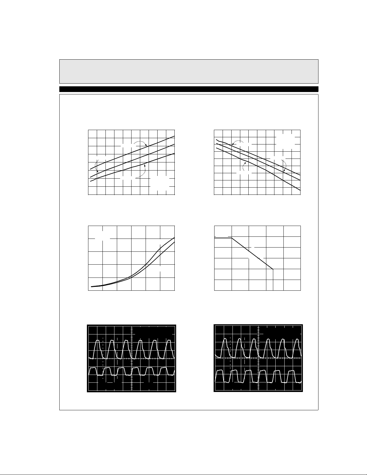
Typical Performance Curves
EL5283C - Preliminary
EL5283C - Preliminary
Dual and Window 8ns High-Speed Comparators
Output Low Voltage vs Load Current
0.31
0.27
TA=25°C
0.23
0.19
Output Low Voltage (V)
0.15
0 102 4 6
Digital Supply Current vs Input Switching Frequency (per
comparator)
50
VS=±5V
T=25°C
40
30
(mA)
SD
I
20
10
0
0 30252015105
TA=85°C
TA=-40°C
Load Current (mA)
Frequency (MHz)
VS=±5V
VSD=5V
VIN=-50mV
8
VSD=5V
VSD=3V
Output High Voltage vs Load Current
4.75
4.7
4.65
4.6
4.55
4.5
4.45
Output High Voltage (V)
4.4
4.35
4.3
0 102 4 6
Package Power Dissipation vs Ambient Temp.
JEDEC JESD51-3 Low Effective Thermal Conductivity Test
0.6
486mW
0.5
0.4
0.3
0.2
Power Dissipation (W)
0.1
0
0 100755025
TA=-40°C
TA=85°C
Load Current (mA)
M
S
O
P
2
1
0
0
6
°
C
/
W
Ambient Temperature (°C)
VS=±5V
VSD=5V
VIN=50mV
TA=25°C
85
8
125
Output with 30MHz Input
VIN=1V
P-P
V
O
V
IN
1V 20ns
Output with 30MHz Input
VIN=3V
P-P
VIN=1V
FIN=30MHz
2V
VS=±5V
P-P
VSD=5V
V
O
V
IN
2V 2V 20ns
VIN=3V
P-P
FIN=30MHz
VS=±5V
VSD=5V
5
Page 6
EL5283C - Preliminary
Dual and Window 8ns High-Speed Comparators
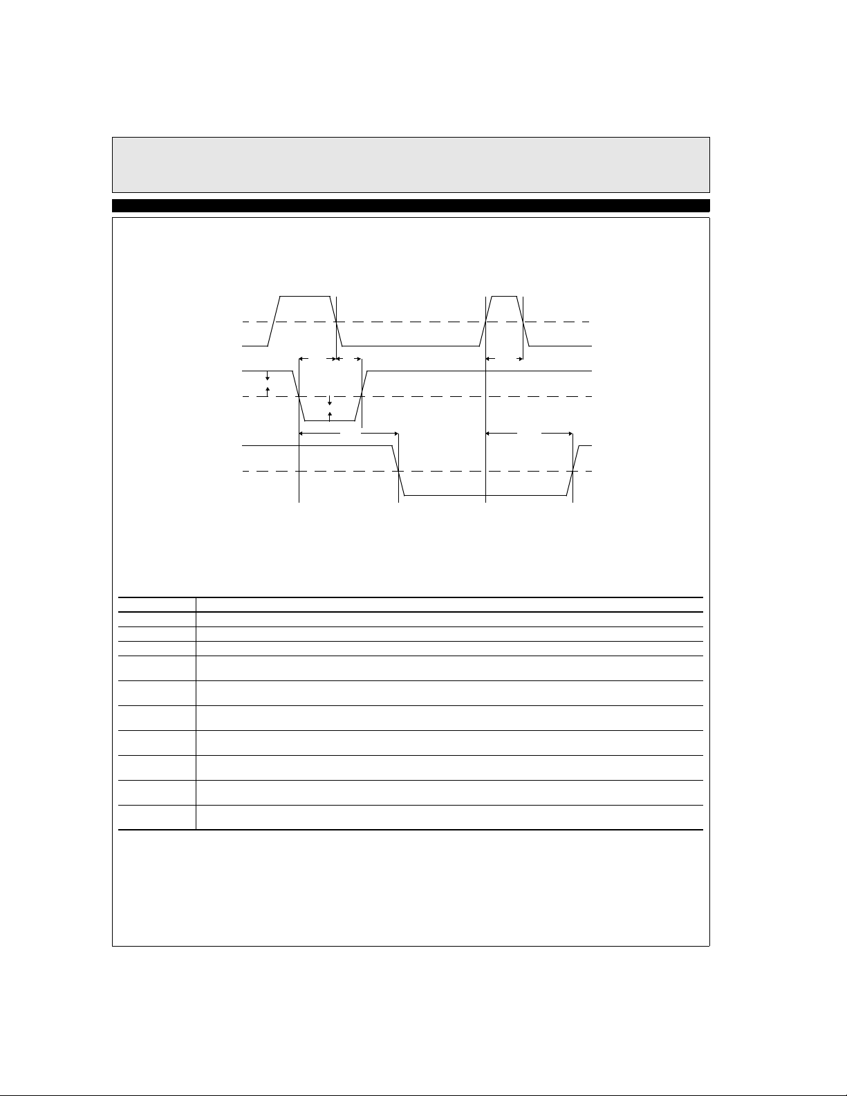
Timing Diagram
EL5283C - Preliminary
Latch
Enable
Input
Latch
Differential
Input
Voltage
Comparator
Output
Compare
Latch Latch
t
t
h
s
V
IN
V
DD
tpd-
Compare
tpw(D)
td+(D)
1.4V
V
2.4V
OS
Definition of Terms
Terms Definition
V
OS
V
IN
V
OD
tpd+ Input to Output High Delay - The propagation delay measured from the time the input signal crosses the input offset voltage to the CMOS
tpd- Input to Output Low Delay - The propagation delay measured from the time the input signal crosses the input offset voltage to the CMOS
td+ Latch Disable to Output High Delay - The propagation delay measured from the latch signal crossing the CMOS threshold in a low to high
td- Latch Disable to Output Low Delay - The propagation delay measured from the latch signal crossing the CMOS threshold in a low to high
t
s
t
h
tpw (D) Minimum Latch Disable Pulse Width - The minimum time that the latch signal must remain high in order to acquire and hold an inpu t signal
Input Offset Voltage - Voltage applied between the two input terminals to obtain CMOS logic threshold at the output
Input Voltage Pulse Amplitude - Usually set to 100mV for comparator specifications
Input Voltage Overdrive - Usually set to 5mV and in opposite polarity to VIN for comparator specifications
logic threshold of an output low to high transition
logic threshold of an output high to low transition
transition to the point of the output crossing CMOS threshold in a low to high transition
transition to the point of the output crossing CMOS threshold in a high to low transition
Minimum Setup Time - The minimum time before the negative transition of the latch signal that an input signal change must be present in
order to be acquired and held at the outputs
Minimum Hold Time - The minimum time after the negative transition of the latch signal that an input signal must remain unchanged in
order to be acquired and held at the output
change
6
Page 7
EL5283C - Preliminary
Dual and Window 8ns High-Speed Comparators
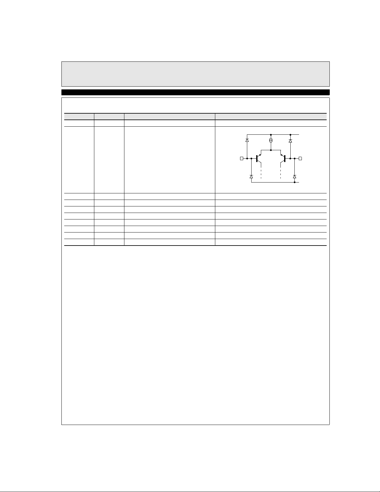
Pin Descriptions
Pin Number Pin Name Function Equivalent Circuit
1 VS+ Positive supply voltage
2 VREFH Upper voltage reference
Circuit 4
3 IN Input (Reference Circuit 4)
4 VREFL Lower voltage reference (Reference Circuit 4)
5 VS- Negative supply voltage
6 GDN Digital ground
7 OUTL Low output (Reference Circuit 2)
8 LATCH Latch (Reference Circuit 3)
9 OUTH High output (Reference Circuit 2)
10 VSD Digital supply voltage
EL5283C - Preliminary
VS+
INVREF
VS-
Applications Information
Power Supplies and Circuit Layout
The EL5283C comparator operates with single and dual
supply with 5V to 12V between VS+ and VS-. The output side of the comparators is supplied by a single
supply from 2.7V to 5V. The rail to rail output swing
enables direct connection of the comparator to both
CMOS and TTL logic circuits. As with many high speed
devices, the supplies must be well bypassed. Elantec recommends a 4.7µF tantalum in parallel with a 0.1µF
ceramic. These should be placed as close as possible to
the supply pins. Keep all leads short to reduce stray
capacitance and lead inductance. This will also minimize unwanted parasitic feedback around the
comparator. The device should be soldered directly to
the PC board instead of using a socket. Use a PC board
with a good, unbroken low inductance ground plane.
Good ground plane construction techniques enhance stability of the comparators.
Input Voltage Considerations
The EL5283C input range is specified from 0.1V below
VS- to 2.25V below VS+. The criterion for the input
limit is that the output still responds correctly to a small
differential input signal. The differential input stage is a
pair of PNP transistors, therefore, the input bias current
flows out of the device. When either input signal falls
below the negative input voltage limit, the parasitic PN
junction formed by the substrate and the base of the PNP
will turn on, resulting in a significant increase of input
bias current. If one of the inputs goes above the positive
input voltage limit, the output will still maintain the correct logic level as long as the other input stays within the
input range. However, the propagation delay will
increase. When both inputs are outside the input voltage
range, the output becomes unpredictable. Large differential voltages greater than the supply voltage should be
avoided to prevent damages to the input stage. Inputs of
unused channels should not be left floating. They should
be driven to a known state. For example, one input can
7
Page 8
EL5283C - Preliminary
Dual and Window 8ns High-Speed Comparators
be tied to ground and the other input can be connected to
some voltage reference (like ±100mV) to avoid oscillation in the output due to unwanted output to input
feedback.
EL5283C - Preliminary
Input Slew Rate
Most high speed comparators oscillate when the voltage
of one of the inputs is close to or equal to the voltage on
the other input due to noise or undesirable feedback. For
clean output waveform, the input must meet certain minimum slew rate requirements. In some applications, it
may be helpful to apply some positive feedback (hysteresis) between the output and the positive input. The
hysteresis effectively causes one comparator's input
voltage to move quickly past the other, thus taking the
input out of the region where oscillation occurs. For the
EL5283C, the propagation delay increases when the
input slew rate increases for low overdrive voltages.
With high overdrive voltages, the propagation delay
does not change much with the input slew rate.
Latch Pin Dynamics
The EL5283C contains a “transparent” latch for each
channel. The latch pin is designed to be driven with
either a TTL or CMOS output. When the latch is connected to a logic high level or left floating, the
comparator is transparent and immediately responds to
the changes at the input terminals. When the latch is
switched to a logic low level, the comparator output
latches remains latched to its value just before the latch
high-to-low transition. To guarantee data retention, the
input signal must remain the same state at least 1ns (hold
time) after the latch goes low and at least 2ns (setup
time) before the latch goes low. When the latch goes
high, the new data will appear at the output in approximately 8ns (latch propagation delay).
Power Dissipation
When switching at high speeds, the comparator's drive
capability is limited by the rise in junction temperature
caused by the internal power dissipation. For reliable
operation, the junction temperature must be kept below
T
(125°C).
JMAX
An approximate equation for the device power dissipation is as follows. Assume the power dissipation in the
load is very small:
P
DISSVSISVSDISD
) N××+×(=
where:
VS is the analog supply voltage from VS+ to VS-
IS is the analog quiescent supply current per comparator
VSD is the digital supply voltage from VSD to ground
I
is the digital supply current per comparator
SD
N is the number of comparators in the package
ISD strongly depends on the input switching frequency.
Please refer to the performance curve to choose the input
driving frequency. Having obtained the power dissipation, the maximum junction temperature can be
determined as follows:
T
JMAXTMAXΘJAPDISS
×+=
where:
T
is the maximum ambient temperature
MAX
θ
is the thermal resistance of the package
JA
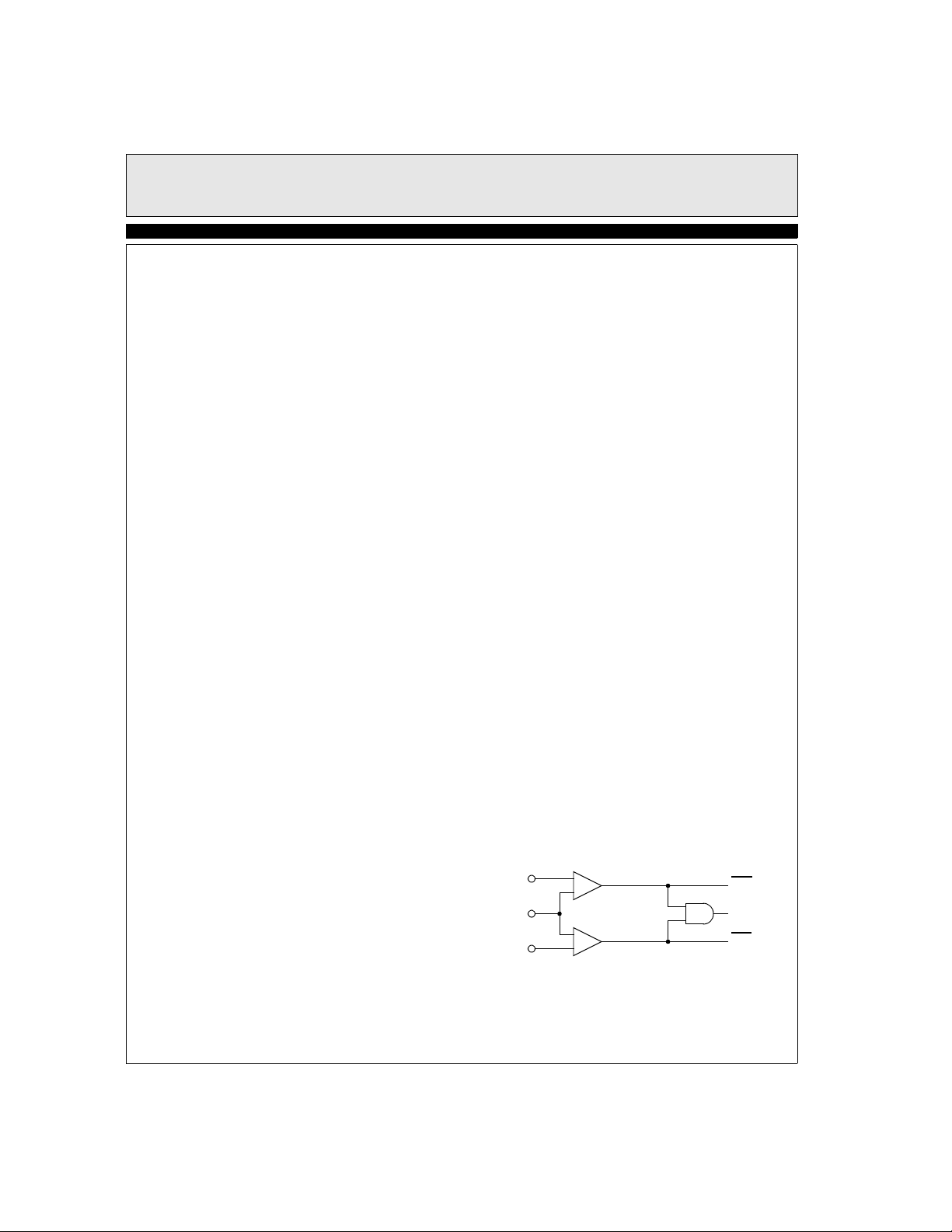
Window Detector
If VIN is in the range of V
puts go high and the input in range is high. If VIN is out
of the range set by V
REFH
is low.
V
REFH
V
IN
V
REFL
+
-
+
-
REFL
and V
< VIN < V
, the input in range
REFL
REFH
, both out-
OUTH
Input In
Range
OUTL
8
Page 9

EL5283C - Preliminary
Dual and Window 8ns High-Speed Comparators
EL5283C - Preliminary
General Disclaimer
Specifications contained in this data sheet are in effect as of the publication date shown. Elantec, Inc. reserves the right to make changes in the circuitry or specifications contained herein at any time without notice. Elantec, Inc. assumes no responsibility for the use of any circuits described
herein and makes no representations that they are free from patent infringement.
WARNING - Life Support Policy
Elantec, Inc. products are not authorized for and should not be used
within Life Support Systems without the specific written consent of
Elantec, Inc. Life Support systems are equipment intended to sup-
Elantec Semiconductor, Inc.
675 Trade Zone Blvd.
Milpitas, CA 95035
Telephone: (408) 945-1323
(888) ELANTEC
Fax: (408) 945-9305
European Office: +44-118-977-6020
Japan Technical Center: +81-45-682-5820
port or sustain life and whose failure to perform when properly used
in accordance with instructions provided can be reasonably
expected to result in significant personal injury or death. Users contemplating application of Elantec, Inc. Products in Life Support
Systems are requested to contact Elantec, Inc. factory headquarters
to establish suitable terms & conditions for these applications. Elantec, Inc.’s warranty is limited to replacement of defective
components and does not cover injury to persons or property or
other consequential damages.
September 6, 2001
9
Printed in U.S.A.
 Loading...