

Page 1
EL5192C
600MHz Current Feedback Amplifier
EL5192C
Features
• 600MHz -3dB band w idth
• 6mA supply current
• Single and dual sup p l y op er a tion,
from 5V to 10V supply span
• Available in 5-pin SOT23 package
• Dual (EL5292C) and triple
(EL5392C) available
• High speed, 1GHz product
available (EL519 1C )
• Low power, 4mA, 300MHz
product available (EL5193C,
EL5293C, and EL5393C)
Applications
• Video Amplifiers
• Cable Drivers
• RGB Amplifiers
• Test Equipment
• Instrumentation
• Current to Voltage Converters
Ordering Information
Part No Package
EL5192CW-T7 5-Pin SOT23 7” MDP0038 EL5192CW-T13 5-Pin SOT23 13” MDP0038 EL5192CS 8-Pin SO - MDP0027 EL5192CS-T7 8-Pin SO 7” MDP0027 EL5192CS-T13 8-Pin SO 13” MDP0027
Tape &
Reel Outline #
General Description
The EL5192C is a current feedback amplifier with a very high bandwidth of 600MHz. This makes this amplifier ideal for today’s high
speed video and monitor applications.
With a supply current of just 6mA and the ability to run from a single
supply voltage from 5V to 10V, th e EL5192C is also ideal for hand
held, portable or battery-powered equipment.
For applications where board space is critical, the EL5192C is offered
in the 5-pin SOT23 package, as well as an industry standard 8-pin SO.
The EL5192C operates over the industrial temperature range of -40°C
to +85°C.
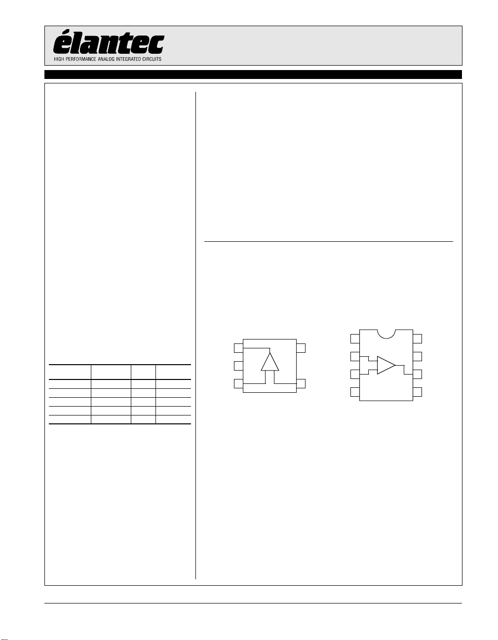
Pin Configurations
8-Pin SO
1
2
-
+
3
-
4
EL5192CS
NC*
8
VS+
7
OUT
6
NC
5
OUT
V
IN+
S
-
1
2
3
5-Pin SOT23
+
-
EL5192CW
NC
+
5
V
S
IN-
4
IN-
IN+
V
S
* This pin must be left disconnected
Note: All information contained in this data sheet has been carefully checked and is believed to be accurate as of the date of publication; however, this data sheet cannot be a “controlled document”. Current revisions, if any, to these
specifications are maintained at the factory and are available upon your request . W e recommend checking the revision level befo re finalization of your design documentation.
© 2001 Elantec Semiconductor, Inc.
April 12, 2001
Page 2
EL5192C
600MHz Current Feedback Amplifier
EL5192C
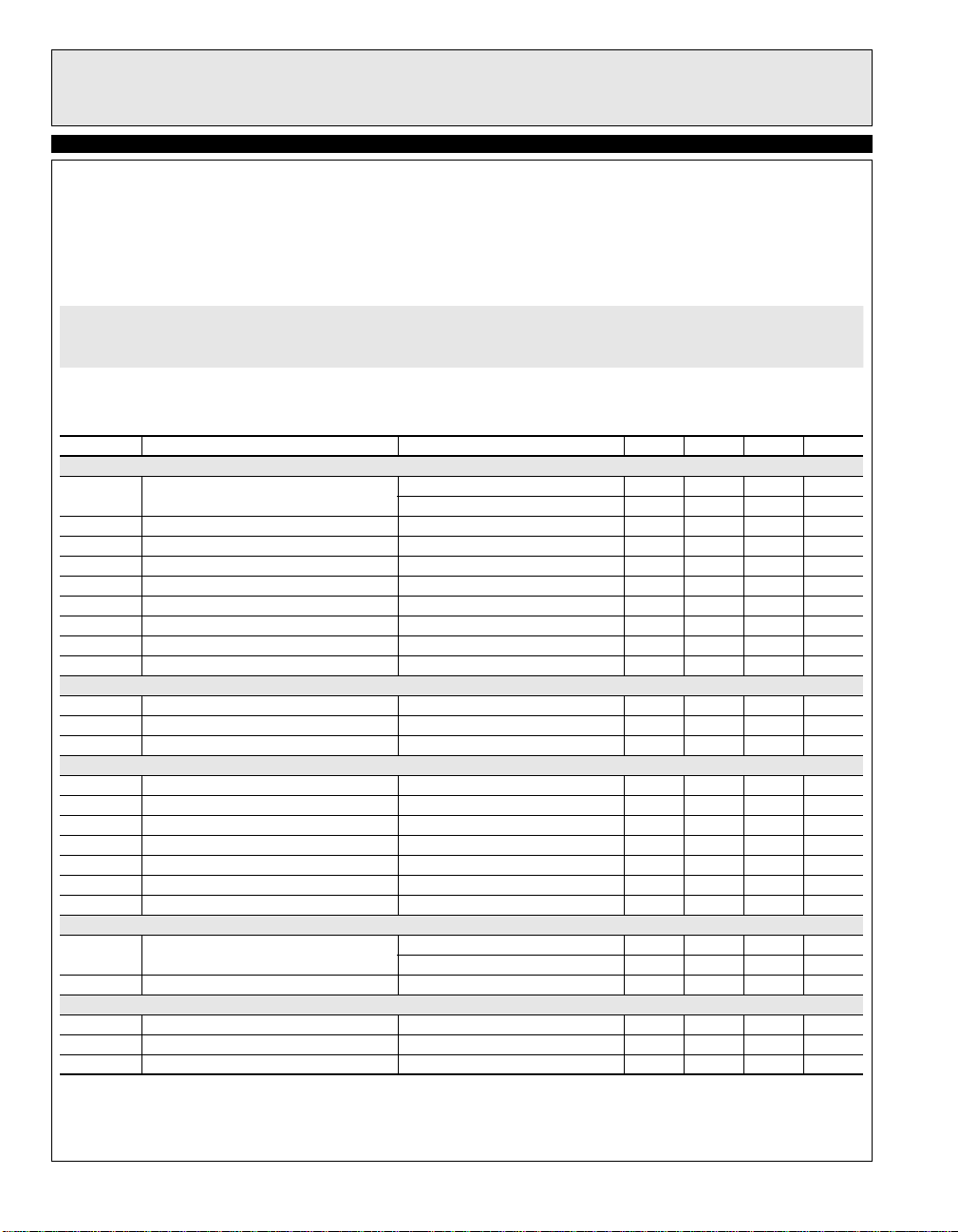
Absolute Maximum Ratings (T
Values beyond absolute maximum ratings can cause the device to be prematurely damaged. Absolute maximum ratings are stress ratings only and
functional device operation is not implied.
Supply Voltage between V
Maximum Continuous Output Current 50mA
+ and VS-11V
S
= 25°C)
A
Operating Junction Temperature 125°C
Power Dissipation See Curves
Pin Voltages V
- - 0.5V to VS+ +0.5V
S
Storage Temperature -65°C to +150°C
Operating Temperature -40°C to +85°C
Important Note:
All parameters having Min/Max specifications are guaranteed. Typ values are for information purposes only. Unless otherwise noted, all tests are at the
specified temperature and are pulsed tests, therefore: T
= TC = TA.
J
Electrical Characteristics
VS+ = +5V, VS- = -5V, RF = 750Ω for AV = 1, RF = 375Ω for AV = 2, RL = 150Ω, TA = 25°C unless otherwise specified.
Parameter Description Conditions Min Typ Max Unit
AC Performance
BW -3dB Bandwidth A
BW1 0.1dB Bandwidth 25 MHz
SR Slew Rate V
ts 0.1% Settling Time V
e
n
i
- IN- input current noise 20 pA/√Hz
n
i
+ IN+ input current noise 50 pA/√Hz
n
dG Differential Gain Error
dP Differential Phase Error
Input Voltage Noise 4.1 nV/√Hz
[1]
[1]
DC Performance
V
T
R
OS
CVOS
OL
Offset Voltage -10 1 10 mV
Input Offset Voltage Temperature Coefficient Measured from T
Transimpedance 200 400 kΩ
Input Characteristics
CMIR Common Mode Input Range ±3 ±3.3 V CMRR Common Mode Rejection Ratio 42 50 dB
-ICMR - Input Current Common Mode Rejection -6 6 µA/V
+I
IN
-I
IN
R
IN
C
IN
+ Input Current -60 3 60 µA
- Input Current -35 2 35 µA
Input Resistance 37 kΩ
Input Capacitance 0.5 pF
Output Characteristics
V
I
OUT
O
Output Voltage Swing RL = 150Ω to GND ±3.4 ±3.7 V
Output Current RL =10Ω to GND 95 120 mA
Supply
Is
ON
Supply Current No Load, V
PSRR Power Supply Rejection Ratio DC, V
-IPSR - Input Current Power Supply Rejection DC, V
1. Standard NTSC test, AC signal amplitude = 286mV
P-P
= +1 600 MHz
V
A
= +2 300 MHz
V
= -2.5V to +2.5V, AV = +2 2500 2800 V/µs
O
= -2.5V to +2.5V, AV = -1 9 ns
OUT
AV = +2 0.015 % AV = +2 0.04 °
to T
MIN
MAX
R
= 1KΩ to GND ±3.8 ±4.0 V
L
= 0V 5 6 7.25 mA
IN
= ±4.75V to ±5.25V 55 75 dB
S
= ±4.75V to ±5.25V -2 2 µA/V
S
5µV/°C
, f = 3.58MHz
2
Page 3
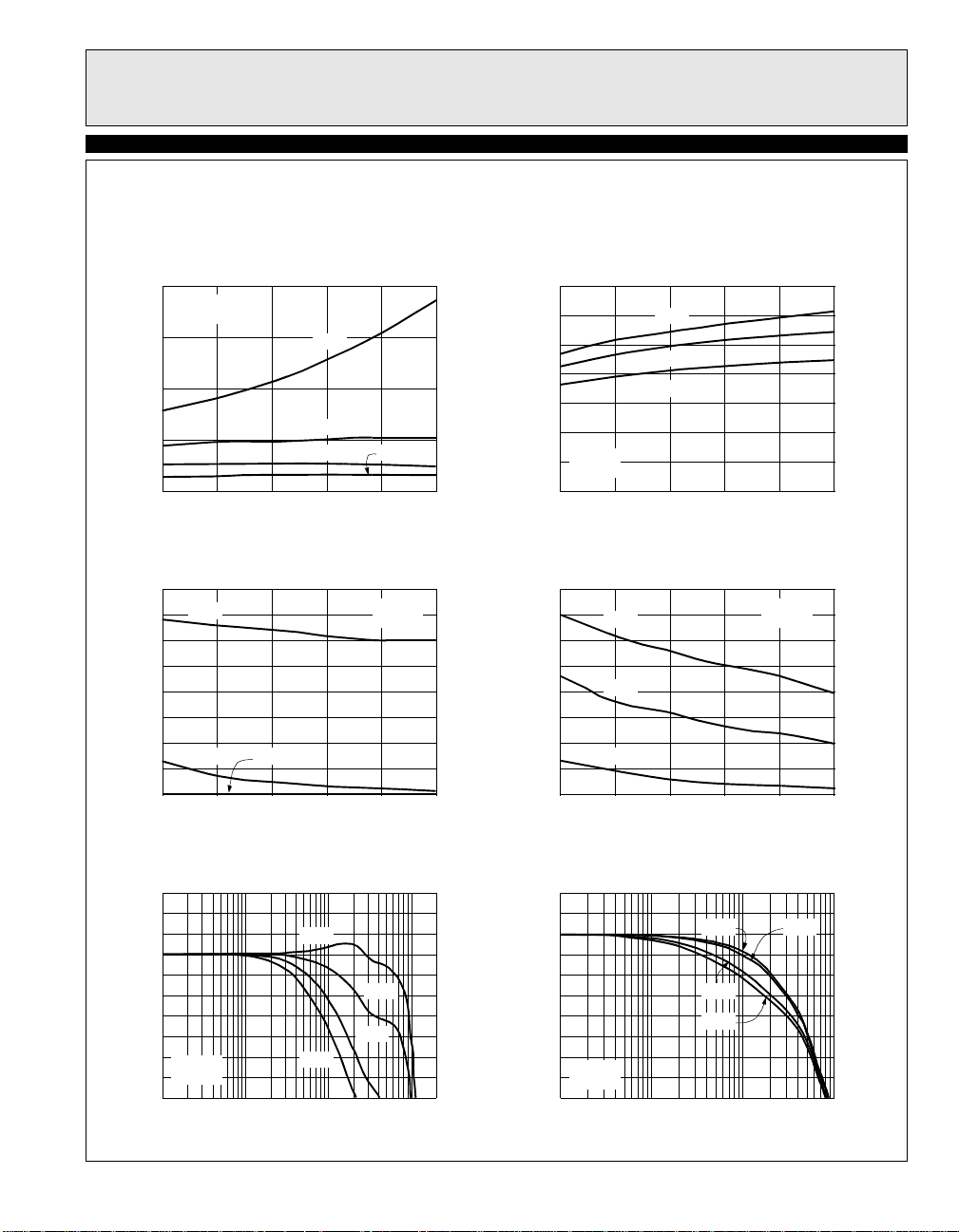
Typical Performance Curves
EL5192C
EL5192C
600MHz Current Feedback Amplifier
Non-Inverting Frequency Response (Gain)
SOT23 Package
6
2
-2
-6
Normalized Magnitude (dB)
-10
RF=750Ω
RL=150Ω
-14
1M 10M 100M 1G
Inverting Frequency Response (Gain)
6
2
-2
-6
Normalized Magnitude (dB)
-10
RF=375Ω
=150Ω
R
L
-14
1M 10M 100M 1G
AV=1
AV=5
AV=10
Frequency (Hz)
AV=-1 AV=-2
AV=-5
Frequency (Hz)
AV=2
Non-Inverting Frequency Response (Phase)
90
0
-90
Phase (°)
-180
-270
RF=750Ω
RL=150Ω
-360
1M 10M 100M 1G
Inverting Frequency Response (Phase)
90
0
-90
Phase (°)
-180
-270
RF=375Ω
=150Ω
R
L
-360
1M 10M 100M 1G
AV=5
AV=10
Frequency (Hz)
AV=-1
AV=-2
AV=-5
Frequency (Hz)
AV=1
AV=2
Frequency Response for Various CIN-
10
2pF added
6
2
-2
Normalized Magnitude (dB)
AV=2
-6
RF=375Ω
RL=150Ω
-10
1M 10M 1G
1pF added
0pF added
100M
Frequency (Hz)
Frequency Response for Various R
6
2
-2
-6
Normalized Magnitude (dB)
-10
AV=2
RF=375Ω
-14
1M 10M 100M 1G
RL=500Ω
Frequency (Hz)
L
RL=100ΩRL=150Ω
3
Page 4
EL5192C
600MHz Current Feedback Amplifier
EL5192C
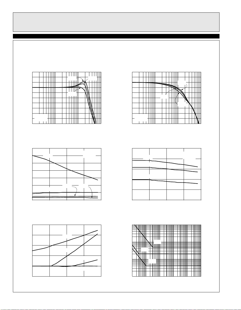
Typical Performance Curves
Frequency Response for Various C
14
10
6
2
Normalized Magnitude (dB)
AV=2
-2
RF=375Ω
RL=150Ω
-6
1M 10M 100M 1G
Frequency (Hz)
Group Delay vs Frequency
3.5
3
2.5
2
1.5
Group Delay (ns)
1
0.5
0
1M 10M 1G
Frequency (Hz)
12pF added
8pF added
0pF added
AV=2
=375Ω
R
F
AV=1
=750Ω
R
F
L
100M
Frequency Response for Various R
6
250Ω 375Ω
2
-2
-6
Normalized Magnitude (dB)
AV=2
-10
RG=R
F
RL=150Ω
-14
1M 10M 100M 1G
Frequency (Hz)
Frequency Response for Various Common-mode
Input Voltages
6
2
-2
-6
Normalized Magnitude (dB)
AV=2
-10
=375Ω
R
F
RL=150Ω
-14
1M 10M 1G
Frequency (Hz)
F
620Ω
750Ω
VCM=3V VCM=0V
VCM=-3V
100M
475Ω
Transimpedance (ROL) vs Frequency
10M
1M
)
Ω
100k
10k
Magnitude (
1k
100
1k
10k 100k 1M 10M 100M 1G
Phase
Gain
Frequency (Hz)
0
-90
-180
-270
-360
PSRR and CMRR vs Frequency
20
0
-20
Phase (°)
-40
PSRR/CMRR (dB)
-60
-80
10k
PSRR-
100k 1M 10M 1G100M
Frequency (Hz)
PSRR+
CMRR
4
Page 5
Typical Performance Curves
EL5192C
EL5192C
600MHz Current Feedback Amplifier
-3dB Bandwidth vs Supply Voltage for Noninverting Gains
800
RF=750Ω
RL=150Ω
600
400
-3dB Bandwidth (MHz)
200
0
567 10
Total Supply Voltage (V)
Peaking vs Supply Voltage for Non-inverting Gains
4
AV=1
3
2
Peaking (dB)
1
AV=2 AV=10
0
567 1089
Total Supply Voltage (V)
AV=1
AV=2
AV=5 AV=10
89
RF=750Ω
RL=150Ω
-3dB Bandwidth vs Supply Voltage for Inverting
Gains
350
300
250
200
150
-3dB Bandwidth (MHz)
100
RF=375Ω
50
RL=150Ω
0
567 1089
Peaking vs Supply Voltage for Inverting Gains
4
3
2
Peaking (dB)
1
0
567 1089
AV=-1
AV=-2
AV=-5
Total Supply Voltage (V)
AV=-1
AV=-2
AV=-5
Total Supply Voltage (V)
RF=375Ω
RL=150Ω
Non-inverting Frequency Response (Gain)
SO8 Package
6
2
-2
-6
Normalized Magnitude (dB)
-10
RF=750Ω
RL=150Ω
-14
1M 10M 100M 1.6G
AV=1
AV=5
AV=10
Frequency (Hz)
AV=2
Non-inverting Frequency Response (Phase)
SO8 Package
90
0
-90
Phase (°)
-180
-270
RF=750Ω
RL=150Ω
-360
1G
1M 10M 100M 1G
AV=1 AV=2
AV=5
AV=10
Frequency (Hz)
5
Page 6
EL5192C
600MHz Current Feedback Amplifier
EL5192C
Typical Performance Curves
Inverting Frequency Response (Gain)
SO8 Package
6
2
-2
-6
Normalized Magnitude (dB)
-10
RF=375Ω
RL=150Ω
-14
1M 10M 100M 1G
-3dB Bandwidth vs Temperature for Non-inverting
Gains
1400
1200
1000
800
600
400
-3dB Bandwidth (MHz)
200
0
AV=1
AV=2
-40 10 60 160
Ambient Temperature (°C)
AV=-1
AV=-5
Frequency (Hz)
AV=5 AV=10
110
AV=-2
RF=750Ω
RL=150Ω
Inverting Frequency Response (Phase)
SO8 Package
90
0
-90
Phase (°)
-180
-270
RF=375Ω
RL=150Ω
-360
1M 10M 100M 1G
-3dB Bandwidth vs Temperature for Inverting
Gains
500
400
300
200
-3dB Bandwidth (MHz)
100
0
AV=-1
AV=-2
AV=-5
-40 10 60 160
AV=-2
Frequency (Hz)
Ambient Temperature (°C)
AV=-1
AV=-5
110
RF=375Ω
RL=150Ω
Peaking vs Temperature
2
RL=150Ω
1.5
1
0.5
Peaking (dB)
0
-0.5
-50 0 50 100
-50
AV=1
AV=-1
Ambient Temperature (°C)
AV=-2
AV=2
Voltage and Current Noise vs Frequency
1000
Hz)
Hz)
√
100
√
10
Voltage Noise (nV/
, Current Noise (pA/
1
100
in+
in-
e
n
1000 10k 100k 10M1M
Frequency ()
6
Page 7

Typical Performance Curves
EL5192C
EL5192C
600MHz Current Feedback Amplifier
Closed Loop Output Impedance vs Frequency
100
10
)
Ω
1
0.1
Output Impedance (
0.01
0.001
100 10k 100M 1G1M
2nd and 3rd Harmonic Distortion vs Frequency
-20
AV=+2
-30
V
=2V
OUT
RL=100Ω
-40
-50
-60
-70
-80
Harmonic Distortion (dBc )
-90
-100
1
P-P
2nd Order
Distortion
100k 10M1k
Frequency (Hz)
3rd Order
Distortion
10 100
Frequency (MHz)
Supply Current vs Supply Voltage
10
8
6
4
Supply Current (mA)
2
0
0
Two-tone 3rd Order
Input Referred Intermodulation Intercept (IIP3)
30
25
20
15
10
5
0
Input Power Intercept (dBm)
-5
AV=+2
=100Ω
R
L
-10
-15
10
Supply Voltage (V)
Frequency (MHz)
AV=+2
=150Ω
R
L
100 200
12210864
Differential Gain/Phase vs DC Input
Voltage at 3.58MHz
0.03
AV=2
0.02
RF=RG=375Ω
RL=150Ω
0.01
0
-0.01
-0.02
dG (%) or dP (°)
-0.03
-0.04
-0.05
-1 -0.5 0 0.5 1
DC Input Voltage
Differential Gain/Phase vs DC Input
Voltage at 3.58MHz
0.03
AV=1
0.02
dP
dG
RF=750Ω
RL=500Ω
0.01
0
-0.01
-0.02
dG (%) or dP (°)
-0.03
-0.04
-0.05
-0.06
-1 -0.5 0 0.5 1
DC Input Voltage
dP
dG
7
Page 8

EL5192C
600MHz Current Feedback Amplifier
EL5192C
Typical Performance Curves
)
PP
Output Voltage Swing (V
200mV/div
Output Voltage Swing vs Frequency
THD<1%
9
8
7
6
5
4
3
2
1
AV=2 AV=2
0
1
Small Signal Step Response Large Signal Step Response
RL=150Ω
RL=500Ω
10 100
Frequency (MHz)
VS=±5V
=150Ω
R
L
AV=2
R
=375Ω
F=RG
Output Voltage Swing vs Frequency
THD<0.1%
10
8
)
PP
Output Voltage Swing (V
1V/div
RL=150Ω
6
4
2
0
1
RL=500Ω
Frequency (MHz)
10 100
VS=±5V
=150Ω
R
L
AV=2
R
=375Ω
F=RG
10ns/div
Settling Time vs Settling Accuracy
25
20
15
10
Settling Time (ns)
5
0
0.01 0.1 1
Settling Accuracy (%)
AV=2
RF=RG=375Ω
RL=150Ω
V
STEP
=5V
P-P
output
10ns/div
Transimpedance (RoI) vs Temperature
500
450
)
Ω
400
RoI (k
350
300
-40 10 60 110 160
Die Temperature (°C)
8
Page 9

Typical Performance Curves
EL5192C
EL5192C
600MHz Current Feedback Amplifier
PSRR and CMRR vs Temperature
90
80
70
60
50
40
PSRR/CMRR (dB)
30
20
10
-40 10 60 110 160
Offset Voltage vs Temperature
3
2
1
(mV)
OS
V
0
-1
-2
-40 10 60 110 160
PSRR
CMRR
Die Temperature (°C)
Die Temperature (°C)
ICMR and IPSR vs Temperature
2.5
2
1.5
1
0.5
ICMR/IPSR (µA/V)
0
-0.5
-1
-40 10 60 110 160
Input Current vs Temperature
60
40
20
0
-20
Input Current (µA)
-40
-60
-80
-40 10 110 160
ICMR+
IPSR
ICMR-
Die Temperature (°C)
60
Temperature (°C)
IB-
IB+
Positive Input Resistance vs Temperature
50
45
40
35
30
)
Ω
25
+ (k
IN
R
20
15
10
5
0
-40 10 160
Temperature (°C)
Supply Current vs Temperature
8
7
6
5
4
3
Supply Current (mA)
2
1
11060
0
-40 10 110 160
60
Temperature (°C)
9
Page 10

EL5192C
600MHz Current Feedback Amplifier
EL5192C
Typical Performance Curves
Positive Output Swin g v s T emper atu re for Var iou s
Loads
4.2
4.1
4
3.9
(V)
OUT
3.8
V
3.7
3.6
3.5
-40 10 50 160
Output Current vs Temperature
135
130
125
(mA)
OUT
I
120
115
-40 10 60 110 160
1kΩ
150Ω
Temperature (°C)
Sink
Source
Die Temperature (°C)
110
Negative Output Swing vs T emperature for Vari ous
Loads
-3.5
-3.6
-3.7
-3.8
(V)
OUT
-3.9
V
-4
-4.1
-4.2
-40 10 110 160
Slew Rate vs Temperature
4600
4400
4200
4000
3800
3600
Slew Rate (V/µS)
3400
3200
3000
-40 10 60 110 160
150Ω
1kΩ
60
Temperature (°C)
Die Temperature (°C)
AV=2
RF=RG=375Ω
RL=150Ω
Maximum Power Dissipation vs Ambient
Temperature
1.4
1.2
1
0.8
0.6
0.4
Power Dissipation (W)
0.2
0
-50 0 50 100
SO8
SOT23
Ambient Temperature (°C)
Package Power Dissipation vs Ambient Temp.
JEDEC JESD51-3 Low Effectiv e Therm al Conductivity Test Board
0.7
T
=150°C
JMAX
625mW
0.6
0.5
391mW
0.4
0.3
0.2
Power Dissipation (W)
0.1
0
0 50 100 150
SO
160
8
°C/W
S
O
T
2
3
5
2
L
5
6
°
C
/
W
25 75 125
Ambient Temperature (°C)
10
Page 11

Pin Descriptions
EL5192C
8-Pin SO
1,5 NC Not connected
EL5192C
5-Pin SOT23
2 4 IN- Inverting input
Pin Name Function Equivalent Circuit
EL5192C
EL5192C
600MHz Current Feedback Amplifier
VS+
IN-IN+
3 3 IN+ Non-inverting input (See circuit 1)
42V
6 1 OUT Output
75V
8 NC Not connected (leave this pin disconnected)
- Negative supply
S
+ Positive supply
S
Circuit1
VS-
VS+
OUT
VS-
Circuit 2
11
Page 12

EL5192C
600MHz Current Feedback Amplifier
EL5192C
Applications Information
Product Description
The EL5192C is a current-feedback operational amplifier that offers a wide -3dB bandwidth of 600MHz and a
low supply current of 6mA per amplifier. The EL5192C
works with supply voltages ranging from a single 5V to
10V and they are also capabl e of swi ngi ng t o wi thin 1 V
of either supply on the output. Because of their currentfeedback topolo gy , t he EL 5 19 2C do es not hav e t he nor mal gain-bandwidth product associated with voltagefeedback operational amp lifiers. Instead, its -3dB bandwidth to remain relatively c onstant as c losed-loop gain is
increased. This combination of high bandwidth and low
power, together with aggressive pricing make the
EL5192C the ideal choice for many low-power/highbandwidth applications such as portable, handheld, or
battery-powered equipment.
For varying bandwidth needs, con sider the EL5191C
with 1GHz on a 9mA supply current or the EL5193C
with 300MHz on a 4mA supply current. Versions
include single, dua l, a nd tri ple amp pa cka ges w ith 5-p in
SOT23, 16-pin QSOP, and 8-pin or 16-pin SO out li nes.
Power Supply Bypassing and Printed Circuit
Board Layout
As with any hig h fr e que ncy d evi ce , good pr in te d c irc uit
board layout is necessary for optimum performance.
Low impedance ground plane construction is essential.
Surface mount components are recommended, but if
leaded components are used, lead lengths should be as
short as possible. The power supply pi ns must be well
bypassed to reduce the risk of os cilla tion. The co mbin ation of a 4.7µF tantalum capacitor in parallel with a
0.01µ F capacitor has been shown to work well when
placed at each supply pin.
For good AC performance, parasitic capacitan ce should
be kept to a minimum, especially at the inverting input.
(See the Capacitance at the Inverting Input section) Even
when ground plane construction i s used, it should be
removed from the area near the inverting input to minimize any stray capacitance at that node. Carbon or
Metal-Film resistors are acceptable with the Metal-Film
resistors giving slightly less peaking and bandwidth
because of additional series inductance. Use of sockets,
particularly for the SO package, should be avoided if
possible. Sockets add parasitic ind uctance and c apacitance which will result in additional peaking and
overshoot.
Capacitance at the Inverting Input
Any manufacturer’s high-speed voltage- or currentfeedback amplifier can b e affected by stra y capacitan ce
at the inverting input. For inverting gains, this parasitic
capacitance has little e ffect because t he inverting i nput is
a virtual ground, but for non- inve rtin g gain s, this ca pacitance (in conjunction with the feedback and gain
resistors) creates a pole in the feedback path of the
amplifier. This pole, if low enough in frequency, has the
same destabilizing effect as a ze ro in the forward openloop response. The use of large-value feedback and gain
resistors exacerbates the problem by further lowering
the pole frequency (increasing the possibility of
oscillation.)
The EL5192C has been optimized with a 375Ω feedback
resistor. With the high bandwidth of these amplifiers,
these resistor values might cause stability problems
when combined with parasitic capacitance, thus ground
plane is not recommende d aroun d the inv erting in put pi n
of the amplifier.
Feedback Resistor Values
The EL5192C has been des ig ned and spec ifi ed at a gai n
of +2 with R
back resistor gives 300MHz of -3dB bandwidth at A
with 2dB of peaking. With A
275MHz of bandwidth with 1dB of peaki ng. Since the
EL5192C is a current-feedback a mplifier, i t is als o possible to change the value of R
As seen in the curve of Frequency Response for Various
RF and RG, bandwidth and pea king can be easily modified by varying the value of the feedback resi stor.
Because the EL5192C is a current-feedback amplifier,
its gain-bandwidth product is not a constant for different
closed-loop gains. This feature actually allows the
EL5192C to maintain about the same -3dB bandwidth.
As gain is increased, bandwidth decreases slightly while
stability increases. Since the loop stability is improving
approximately 375Ω. This value of feed-
F
=-2, an RF of 375Ω gives
V
to get more bandwidth.
F
=2
V
12
Page 13

EL5192C
600MHz Current Feedback Amplifier
EL5192C
with higher closed-loop gains, it becomes possible to
reduce the value of R
still retain stability, resulting in only a slight loss of
bandwidth with inc reased closed-loop gain.
below the specified 375Ω and
F
Supply Voltage Range and Single-Supply
Operation
The EL5192C has been designed to operate with supply
voltages having a span of greater than 5V and less than
10V. In practical terms, this means that the EL5192C
will operate on dual supplies ranging from ±2.5V to
±5V. With single-supply, the EL5192C will operate
from 5V to 10V.
As supply voltages continue to decrease, it becomes necessary to provide input and output voltage ranges that
can get as close as possible to the supply voltages. The
EL5192C has an input ran ge which e xtends to with in 2V
of either supply. So, for example, on ±5V supplies, the
EL5192C has an input ran ge wh ic h span s ±3V. The output range of the EL5192C is also quite large, extending
to within 1V of the supply rail. On a ±5V supply, the
output is therefore capable of swinging from -----4V to
+4V. Single-sup ply output range is larger because of the
increased negative swing due to the external pull-down
resistor t o gr o u n d.
Video Performance
For good video performance, an amplifier is required to
maintain the same output impedance and the same frequency response as DC level s are changed at the output.
This is especially difficult when driving a standard vid eo
load of 150Ω, because of the change in output current
with DC level. Previously, good differential gain could
only be achieved by running high idle currents through
the output transistors (to reduce variations in output
impedance.) These currents were typically comparable
to the entire 6mA supply current of each EL5192C
amplifier. Special circuitry has been incorporated in the
EL5192C to reduce the variation of output impedance
with current output. This results in dG and dP specifications of 0.015% and 0.04°, while driving 150 Ω at a gain
of 2.
Video performance has also been measured with a 500Ω
load at a gain of +1. Under these conditions, the
EL5192C has dG and dP specifications of 0.03% and
0.05°, respectively.
Output Drive Capability
In spite of its low 6mA of supply current, the EL5192C
is capable of providin g a minimu m of ±95mA of ou tput
current. With a minimum of ±95mA of output drive, the
EL5192C is capable of driving 50Ω loads to both rails,
making it an excellent choice for driving isolation transformers in telecommunications applications.
Driving Cables and Capacitive Loads
When used as a cable driver, double termination is
always recommended for reflection-free perfo rmance.
For those applications, the back-term ina tion series re sistor will decouple the EL5192C from the c ab le an d allo w
extensive capacitive drive. However, other applications
may have high capaci tiv e loa ds wit hout a b ack -te rmination resistor. In these applications, a small series resist or
(usually between 5Ω and 50Ω) can be placed in series
with the output to eliminate most peaking. The gain
resistor (R
loss which may be created by this additional resistor at
the output. In many cases it is also possible to simply
increase the value of the feedback resistor (R
the peaking.
) can then be c hosen to make up for any ga in
G
) to reduce
F
Current Limiting
The EL5192C has no internal current-limiting circuitry.
If the output is shorted, it is possible to ex ceed the Abso lute Maximum Rating for o utput current or power
dissipation, potentially resultin g in the d estr uctio n o f th e
device.
Power Dissipation
With the high output drive ca p ability of the EL5192C, it
is possible to exceed the 125°C Absolute Maximum
junction temperature under certain very high load current conditions. Generally speaking when R
about 25Ω, it is important to calculate the maximum
junction temperature (T
determine if power supply voltages, load conditions, or
package type need t o be modified for the EL 5192C to
) for the application to
JMAX
falls below
L
13
Page 14

EL5192C
600MHz Current Feedback Amplifier
EL5192C
remain in the safe operating area. These parameters are
calculated as follows:
T
JMAXTMAXθJA
nPD
××()+=
where:
0D[LPXP$PELHQW7HPSHUDWXUH
7
0$;
θ
7KHUPDO5HVLVWDQFHRIWKH3DFNDJH
-$
Q 1XPEHURI$PSOLILHUVLQWKH3DFNDJH
0D[LPXP3RZHU'LVVLSDWLRQRI(DFK
3'
0$;
$PSOLILHULQWKH3DFNDJH
PD
for each amplifier can be calculated as follows:
MAX
PD
MAX
2( VSI
SMAX
) VS( V
OUTMAX
where:
96 6XSSO\9ROWDJH
0D[LPXP6XSSO\&XUUHQWRI$
,
60$;
9
2870$;
5
/
0D[LPXP2XWSXW9ROWDJH5HTXLUHG
/RDG5HVLVWDQFH
MAX
V
----------------------------
)
×–+××=
OUTMAX
R
L
14
Page 15

Typical Application Circuits
Inverting 200mA Output Current Distribution Amplifier
EL5192C
EL5192C
600MHz Current Feedback Amplifier
+5V
IN+
IN-
-5V
+5V
IN+
IN-
-5V
375Ω 375Ω
V
IN
Fast-Settling Precision Amplifier
375Ω 375Ω
375Ω
0.1µF
V
+
S
OUT
VS-
0.1µF
375Ω 5Ω
0.1µF
VS+
OUT
V
-
S
0.1µF
VS+
VS-
0.1µF
OUT
0.1µF
+5V
IN+
IN-
-5V
V
OUT
5Ω
VS+
VS-
0.1µF
0.1µF
OUT
V
OUT
375Ω
V
IN
+5V
IN+
IN-
-5V
15
Page 16

EL5192C
600MHz Current Feedback Amplifier
EL5192C
Typical Application Circuits
Differential Line Driver/Receiver
V
IN
+5V
IN+
IN-
-5V
375Ω 162Ω
+5V
IN+
IN-
-5V
375Ω 375Ω
0.1µF
+
V
S
OUT
VS-
0.1µF
V
+
OUT
0.1µF
+
V
S
OUT
V
-
S
0.1µF
162Ω
V
-
OUT
0.1µF
1kΩ
240Ω
0.1µF
1kΩ
+5V
IN+
IN-
-5V
375Ω
+5V
IN+
IN-
-5V
375Ω 375Ω
375Ω
ReceiverTransmitter
0.1µF
+
V
S
OUT
VS-
0.1µF
0.1µF
+
V
S
OUT
V
-
S
0.1µF
V
OUT
16
Page 17

EL5192C
600MHz Current Feedback Amplifier
EL5192C
General Disclaimer
Specifications contained in this data sheet are in effect as of the publicat ion date shown. Elantec, Inc. re serves the r ight to make changes in th e circuitry or specifications cont ained herein at a ny time without notice. Elantec , Inc. assumes no res ponsibili ty for t he us e of an y circuits descr ibed
herein and makes no representations that they are free from patent infringement.
WARNING - Life Support Policy
Elantec, Inc. products are not authorized for and should not be used
within Life Support Systems without the specific written consent of
Elantec, Inc. Life Support systems are equipment intend ed to sup-
Elantec Semiconductor, Inc.
675 Trade Zone Blvd.
Milpitas, CA 95035
Telephone: (408) 945-1323
Fax: (408) 945-9305
European Office: +44-118-977-6020
Japan Technical Center: +81-45-682-5820
April 12, 2001
(888) ELANTEC
port or sustain life and whose failure to perform when properly used
in accordance with instructions provided can be reasonably
expected to result in significant personal injury or death. Users contemplating applicatio n of Elantec, Inc. P roducts in Li fe Support
Systems are requested to contact Elantec, Inc. factory headquarters
to establish suitable terms & conditions for these applications. Elantec, Inc. ’s warranty is limited to replacement of defective
components and does not cov er injury to persons or prop erty or
other consequential damages.
17
Printed in U.S.A.
 Loading...