

Page 1

EL4083C
Current Mode Four Quadrant Multiplier
EL4083C December 1995 Rev B
Features
# Novel current mode design
Virtual ground current summing
inputs
Differential ground referenced
current outputs
# High speed (both inputs)
200 MHz bandwidth
12 ns 1% settling time
# Low distortion
k
THD
THD
# Low noise (R
0.03%@1 MHz
k
0.1%@10 MHz
e
L
50X)
100 dB dynamic range
10 Hz to 20 kHz
73 dB dynamic range
10 Hz to 10 MHz
# Wide supply conditions
g
5tog15V operation
Programmable bias current
# 0.2 dB gain tolerance to 25 MHz
Applications
# Four quadrant multiplication
# Gain control
# Controlled signal summing and
multiplexing
# HDTV video fading and
switching
# Mixing/modulating/
demodulating (phase detection)
# Frequency doubling
# Division
# Squaring
# Square rooting
# RMS and power measurement
# Vector addition-RMS summing
# CRT focus and geometry
correction
# Polynomial function generation
# AGC circuits
General Description
The 4083C makes use of an Elantec fully complimentary oxide
isolated bipolar process to produce a patent pending current in,
current out four quadrant multiplier. Input and output signal
summing and direct interface to other current mode devices can
be accomplished by simple connection to reduce component
count and preserve bandwidth. The selection of an appropriate
series resistor value allows an input to accept a voltage signal of
any size and optimize dynamic range. The differential outputs
offer significant performance improvements which greatly extend the usable gain control range at high frequencies. The bias
current is programmable to accommodate the voltage and power dissipation constraints of the package and available systems
supplies.
The devices can implement all the classic four quadrant multiplier applications and are uniquely well suited to gain control
and signal summing of broadband signals.
Connection Diagram
EL4083
8-Pin SO/P DIP
4083– 1
Top View
Ordering Information
Part No. Temp. Range Package Outline
EL4083CNb40§Ctoa85§C 8-Pin P-DIP MDP0031
EL4083CSb40§Ctoa85§C 8-Pin SO MDP0027
Note: All information contained in this data sheet has been carefully checked and is believed to be accurate as of the date of publication; however, this data sheet cannot be a ‘‘controlled document’’. Current revisions, if any, to these
specifications are maintained at the factory and are available upon your request. We recommend checking the revision level before finalization of your design documentation.
©
1993 Elantec, Inc.
Ý
Manufactured under U.S. Patent No. 5,389,840
Page 2
EL4083C
Current Mode Four Quadrant Multiplier
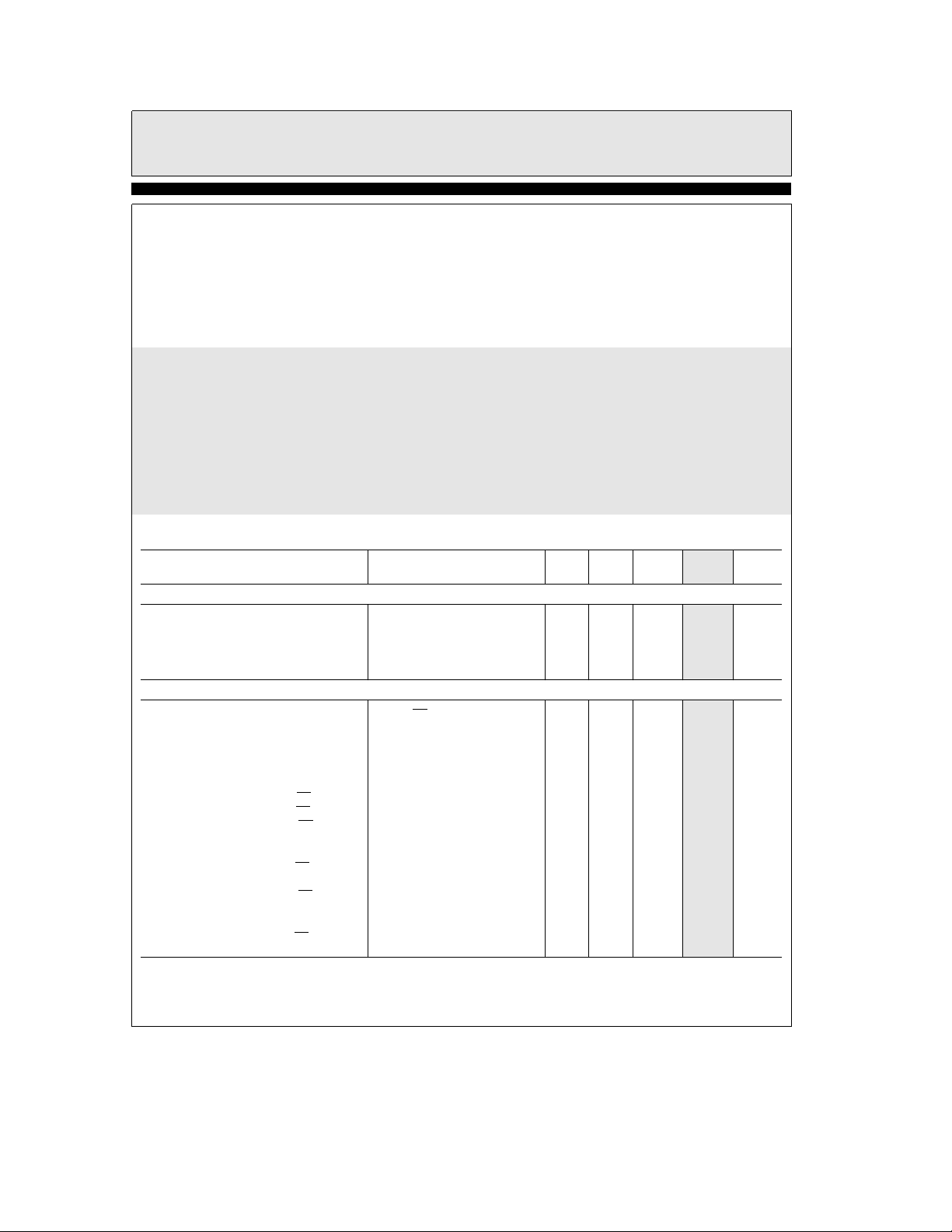
Absolute Maximum Ratings
T
MAX
a
S
and T
V
I
I
I
P
T
Important Note:
All parameters having Min/Max specifications are guaranteed. The Test Level column indicates the specific device testing actually
performed during production and Quality inspection. Elantec performs most electrical tests using modern high-speed automatic test
equipment, specifically the LTX77 Series system. Unless otherwise noted, all tests are pulsed tests, therefore T
Test Level Test Procedure
Voltage between V
S
Z, Bias Current
Z(BIAS)
X Input Current
X
Y Input Current
Y
Maximum Power Dissipation See Curves
D
Operating Temperature Range
A
EL4083
I 100% production tested and QA sample tested per QA test plan QCX0002.
II 100% production tested at T
III QA sample tested per QA test plan QCX0002.
IV Parameter is guaranteed (but not tested) by Design and Characterization Data.
V Parameter is typical value at T
ba
and V
S
b
40§Ctoa85§C
A
per QA test plan QCX0002.
MIN
Electrical Characteristics
Parameter Conditions Min Typ Max
e
(T
25§C)
A
33V
a
2.4 mA
g
2.4 mA
g
2.4 mA
e
25§C and QA sample tested at T
e
25§C for information purposes only.
A
e
(T
25§C, V
A
T
T
e
g
5, I
S
Operating Junction Temperature
J
EL4083 150
Storage Temperature
ST
J
e
25§C,
A
e
1.6 mA) unless otherwise specified
Z
b
65§Ctoa150§C
e
e
T
TA.
C
Test
Level
§
Units
C
Power Supplies
Operating Supply Voltage Range
I
CC
I
CC
I
EE
I
EE
g
e
g
V
S
e
g
V
S
e
g
V
S
e
g
V
S
15V, I
5V, I
15V, I
5V, I
e
0.2 mA 7.2 8.5 9.5 I mA
Z
e
1.6 mA 42.0 44.0 45 I mA
Z
e
0.2 mA 9.5 10.0 12 I mA
Z
e
1.6 mA 45 47 48 I mA
Z
4.5
g
16.5 I V
Multiplier Performance
Transfer Function (Note 5) (IXY–IXY)eK(I
K Value 0.92 0.965 1.01 I
b
Total Error (Note 1)
vs. Temp T
Linearity (Note 2) 0.25 0.5 I %FS
Bandwidth (Note 3)
X Feedthrough DC to I
Y Feedthrough DC to IXYor IXY(Note 5) I
AC Feedthrough, X to I
AC Feedthrough, X to (I
AC Feedthrough, Y to I
or IXY(Note 5) I
XY
or IXY(Note 4) I
XY
) (Note 4) I
XY–IXY
or IXY(Note 4) I
XY
2mAkIX,I
to T
MIN
MAX
b
3 dB (See Figure 2) 200 225 III MHz
e
g
2 mA, I
X
e
g
2 mA, I
Y
e
4 mApp, I
X
e
3.58 MHz
f
e
100 MHz
f
e
4 mApp, I
X
kfk
e
Y
e
3.58 MHz
1 GHz
4 mApp, I
DC
f
fe100 MHz
AC Feedthrough, Y to (I
XY–IXY
) (Note 4) I
DC
Y
e
4 mApp, I
kfk
1 GHz
c
IY)/I
X
k
Y
e
Y
e
X
e
Y
e
Y
e
X
e
X
Z
2mA
g
g
0.5
1.5
g
2 I %FS
g
3 IV %FS
0 (unnulled) 0.15 1.6 I %FS
0 (unnulled) 0.15 1.6 I %FS
nulled
b
80 V dB
b
nulled
28 V dB
b
50 V dB
nulled
b
64 V dB
b
26 V dB
nulled
b
50 V dB
TDis3.7in
2
Page 3
EL4083C
Current Mode Four Quadrant Multiplier
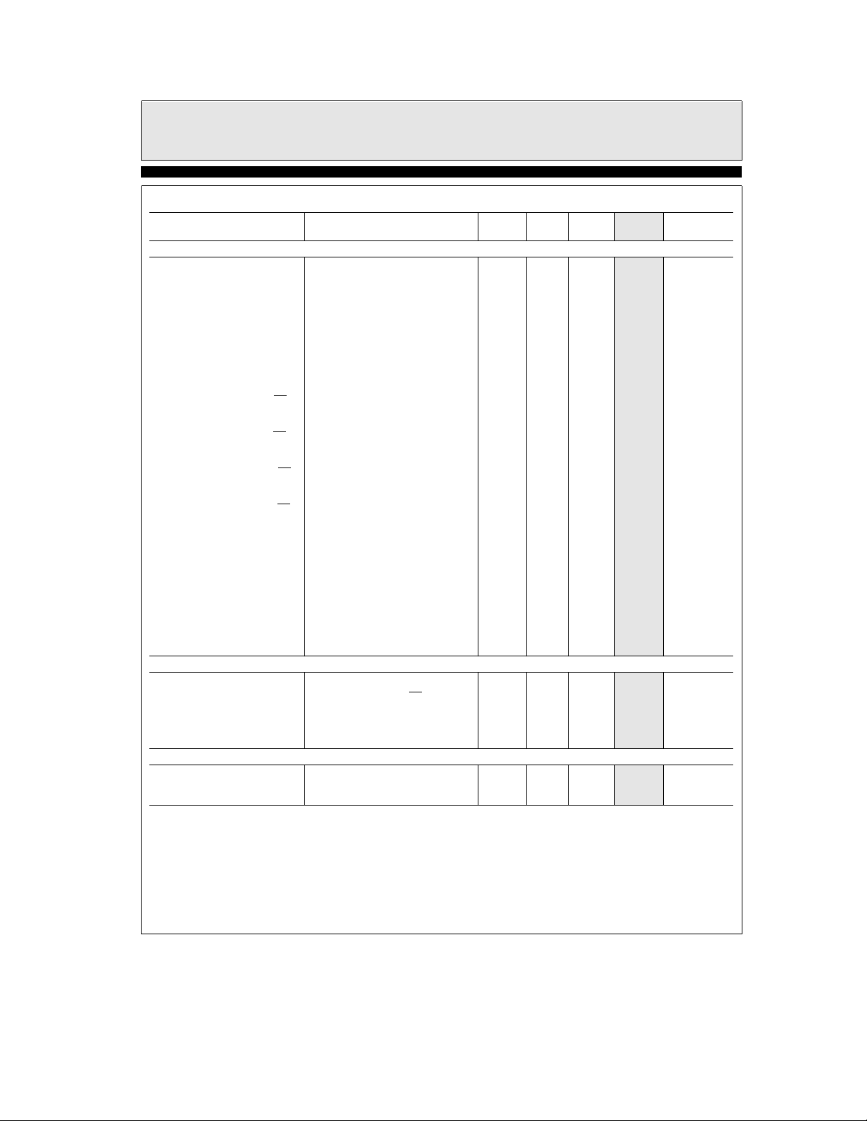
Electrical Characteristics
Parameter Conditions Min Typ Max
Ð Contd. (T
e
A
25§C, V
e
S
e
g
5, I
1.6 mA) unless otherwise specified
Z
Test
Level
Units
Inputs (IX,IY)
Full Scale Range FRSe1.25cIZ(Nominal)
Clipping Level C
Z
)304048IX
IN(IX
Z
)303648IX
IN(IY
Input Offset Voltages at Input Pins, I
(V
OSX,VOSY
Input Offset Currents (Note 5) R
I
XOS,IYOS
Nonlinearity
I
X
I
Y
Distortion, I
Distortion, I
Distortion, I
Distortion, I
)I
(to IXYor IXY)I
X
(to IXYor IXY)I
Y
b
X
Y
(to (I
(to (I
IXY)I
XY
b
IXY)I
XY
Diff Gain
I
X
I
Y
I
X
I
Y
Diff Phase
I
X
I
Y
I
X
I
Y
e
2cI
L
Z
SX
T
MIN
I
Y
I
X
Y
e
f
e
f
X
e
f
fe100 MHz
Y
e
f
e
f
X
e
f
e
f
@
3.58 MHz
I
Z
I
Z
I
Z
I
Z
@
3.58 MHz
I
Z
I
Z
I
Z
I
Z
Z
e
1.6 mA
e
0.2 mA
e
e
2 mA,b2mAkI
e
e
2 mA,b2mAkI
Z
e
R
1K, V
SY
to T
MAX
2 mA,b2mAkI
3.58 MHz
100 MHz
e
2 mA,b2mAkIyk2mA
3.58 MHz
e
2 mA,b2mAkI
3.58 MHz
100 MHz
e
2 mA,b2mAkI
3.58 MHz
100 MHz
e
0.2 mA, I
e
0.2 mA, I
e
1.6 mA, I
e
1.6 mA, I
e
0.2 mA, I
e
0.2 mA, I
e
1.6 mA, I
e
1.6 mA, I
e
0.25 mA 0.2 V %
Y
e
0.25 mA 0.17 V %
X
e
2 mA 0.1 V %
Y
e
2 mA 0.05 V %
X
e
0.25 mA 0.5 V deg
Y
e
0.25 mA 0.5 V deg
X
e
2 mA 0.05 V deg
Y
e
2 mA 0.05 V deg
X
2.85 3.2 I mA
b
e
e
V
X
Y
k
2 mA 0.1 0.6 I %FS
X
k
2 mA 0.1 0.4 I %FS
Y
k
2mA
X
k
2mA
X
k
2mA
Y
b
0,
g
2ImA
4
12
g
g
b
b
b
b
b
b
b
b
a
4mV
a
12 mV
g
10
40 I mA
20 V nA/§C
55 V dB
25 V dB
56 V dB
26 V dB
66 V dB
35 V dB
66 V dB
34 V dB
§
§
§
§
Outputs (IXY,IYX)
Output IOS(Note 5) I
Diff Output I
Voltage Compliance
(Note 5) I
OS
Max Output Current Swing
Noise Spectral Density
kfk
10 Hz
10 MHz R
e
I
X
X
L
0
Y
e
e
I
0, (IXY–IXY)
Y
e
50X 125 V pA/rootHz
g
g
1.5
2.85
b
g
15
g
0.1
g
2.0 V V
g
3.2 I mA
120 I mA
g
80 I mA
e
IZ(Bias)
Current Range Tested 0.2 1.6 I mA
Input Voltage I
Input Voltage I
Note 1: Error is defined as the maximum deviation from the ideal transfer function expressed as a percentage of the full scale
output.
Note 2: Linearity is defined as the error remaining after compensating for scale factor (gain) variation and input and output referred
offset errors.
e
0.2 mA
Z
e
1.6 mA
Z
g
25 I mV
g
25 I mV
Note 3: Bandwidth is guaranteed using the squaring mode test circuit of Figure 4.
Note 4: Relative to full scale output with full scale sinewave on signal input and zero port input nulled. Specification represents
feedthrough of the fundamental.
Note 5: Specifications are provisional for the EL4083.
TDis5.8in
3
Page 4
EL4083C
Current Mode Four Quadrant Multiplier
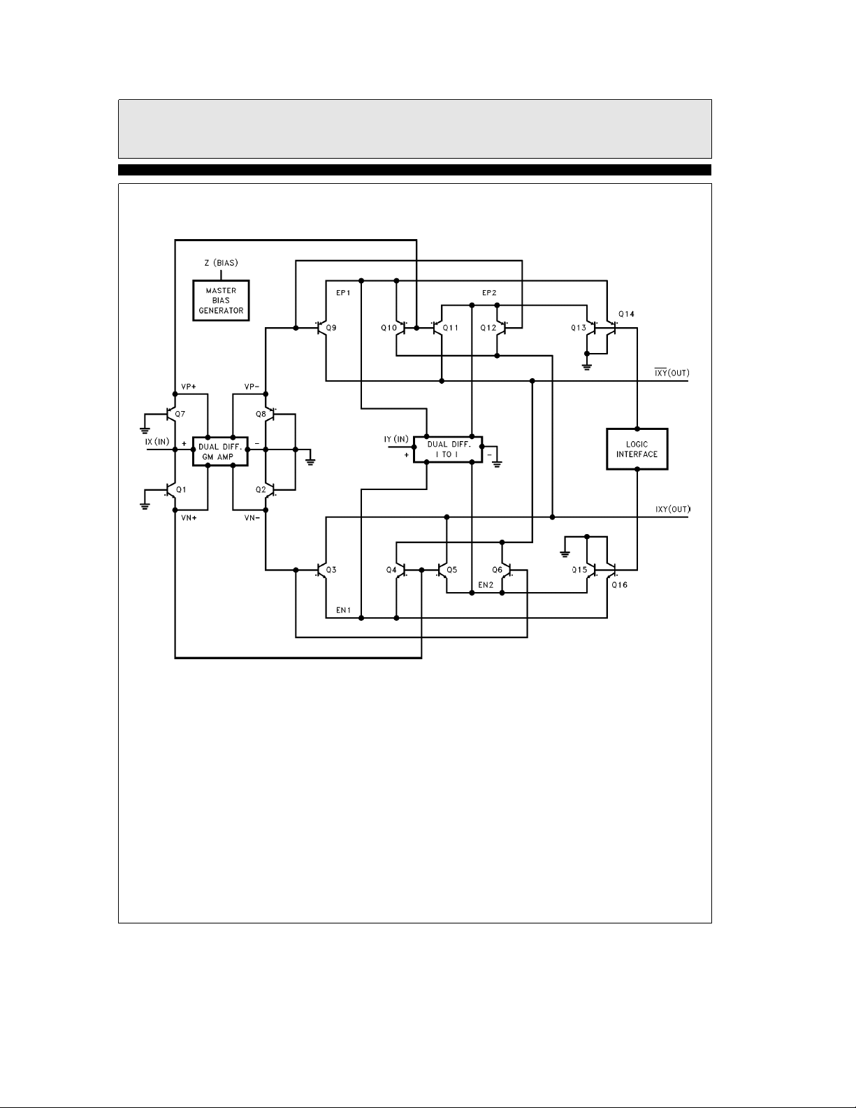
EL4083 Block Diagram
Figure 1
4
4083– 3
Page 5
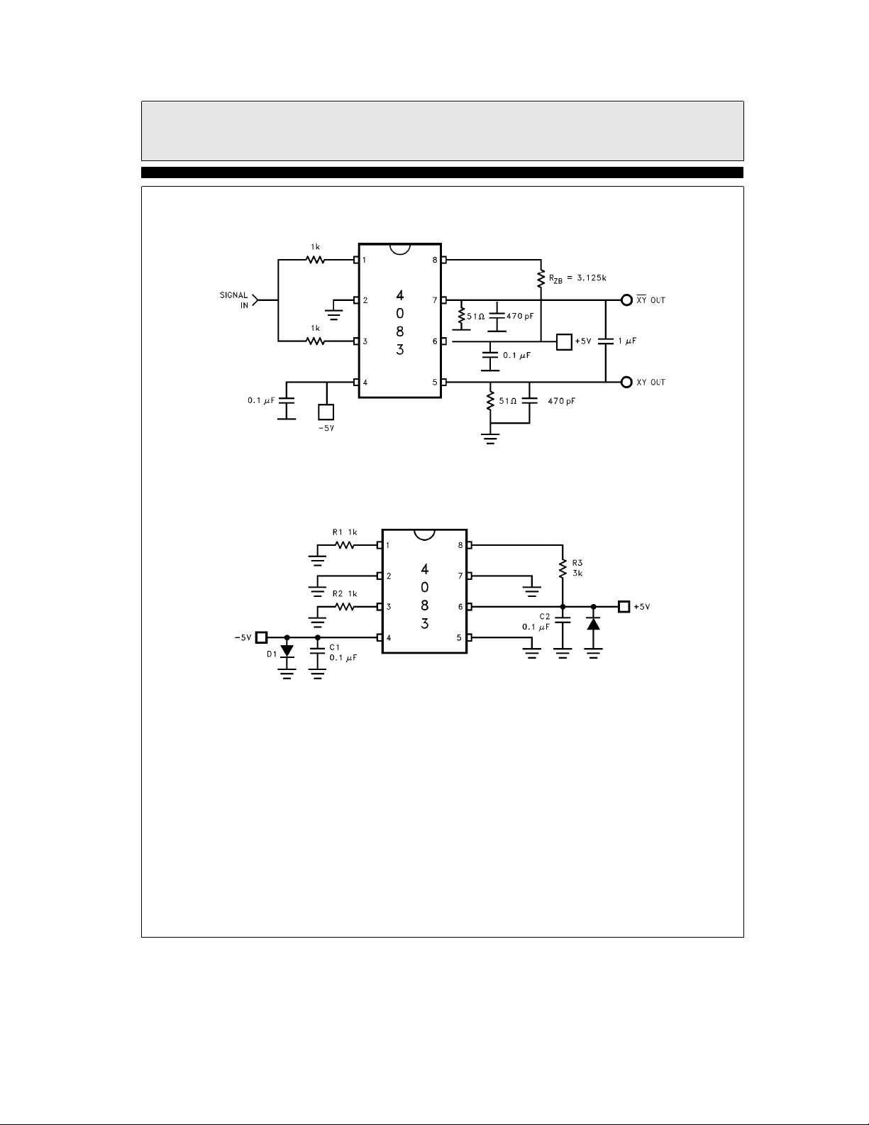
AC Test Fixture
EL4083C
Current Mode Four Quadrant Multiplier
Burn-In Circuit
Figure 2. AC Bandwidth Test Fixture
Top View
Figure 3. Burn-In Circuit P-DIP
4083– 5
4083– 4
5
Page 6
EL4083C
Current Mode Four Quadrant Multiplier
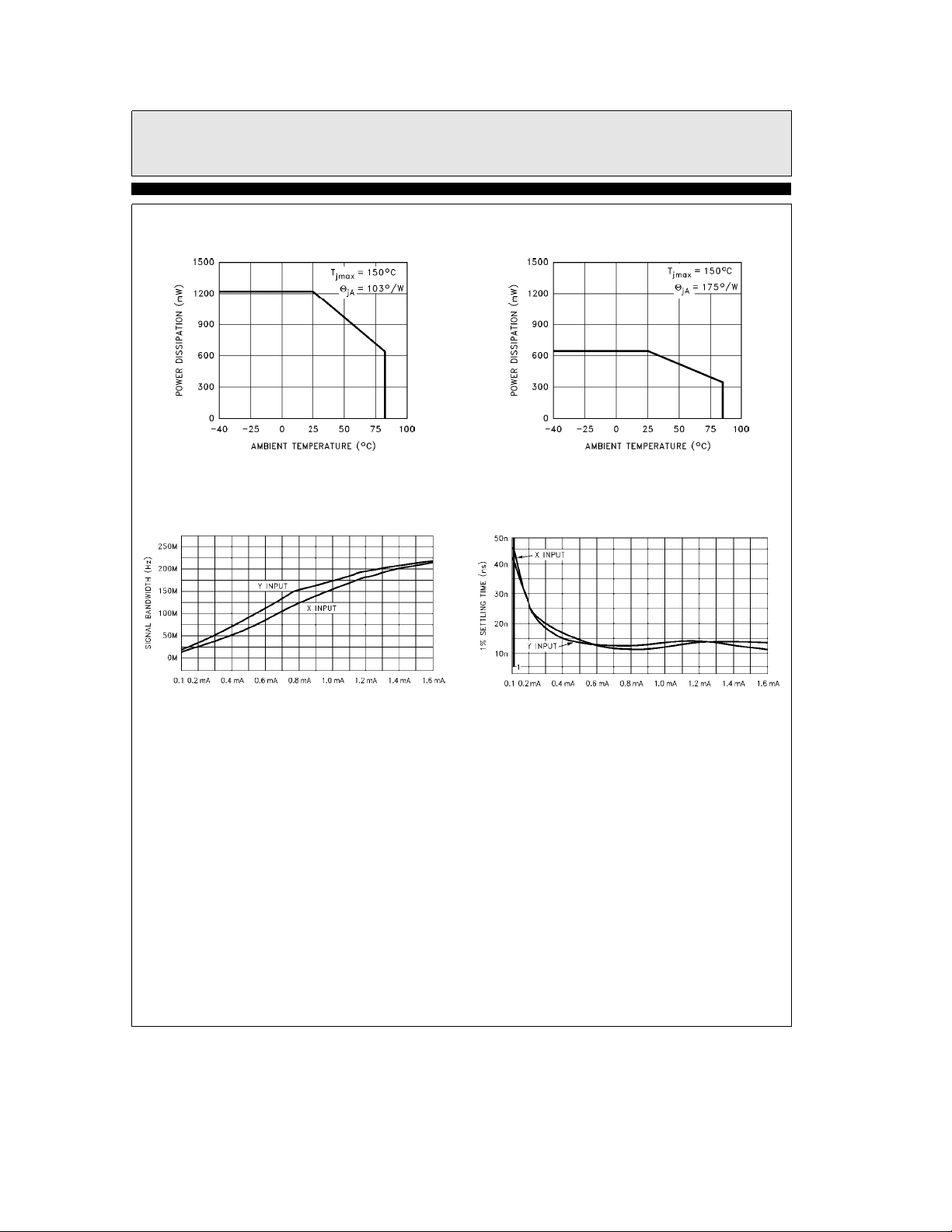
8-Pin Plastic DIP
Maximum Power Dissipation
vs Ambient Temperature
Figure 4
4083– 6
8-Lead SO
Maximum Power Dissipation
vs Ambient Temperature
Figure 5
4083– 7
Figure 6. (IX,IYBandwidth vs IZ)
4083– 10
Figure 7. (IX,IY1% Settling Time vs IZ)
4083– 11
6
Page 7
EL4083C
Current Mode Four Quadrant Multiplier
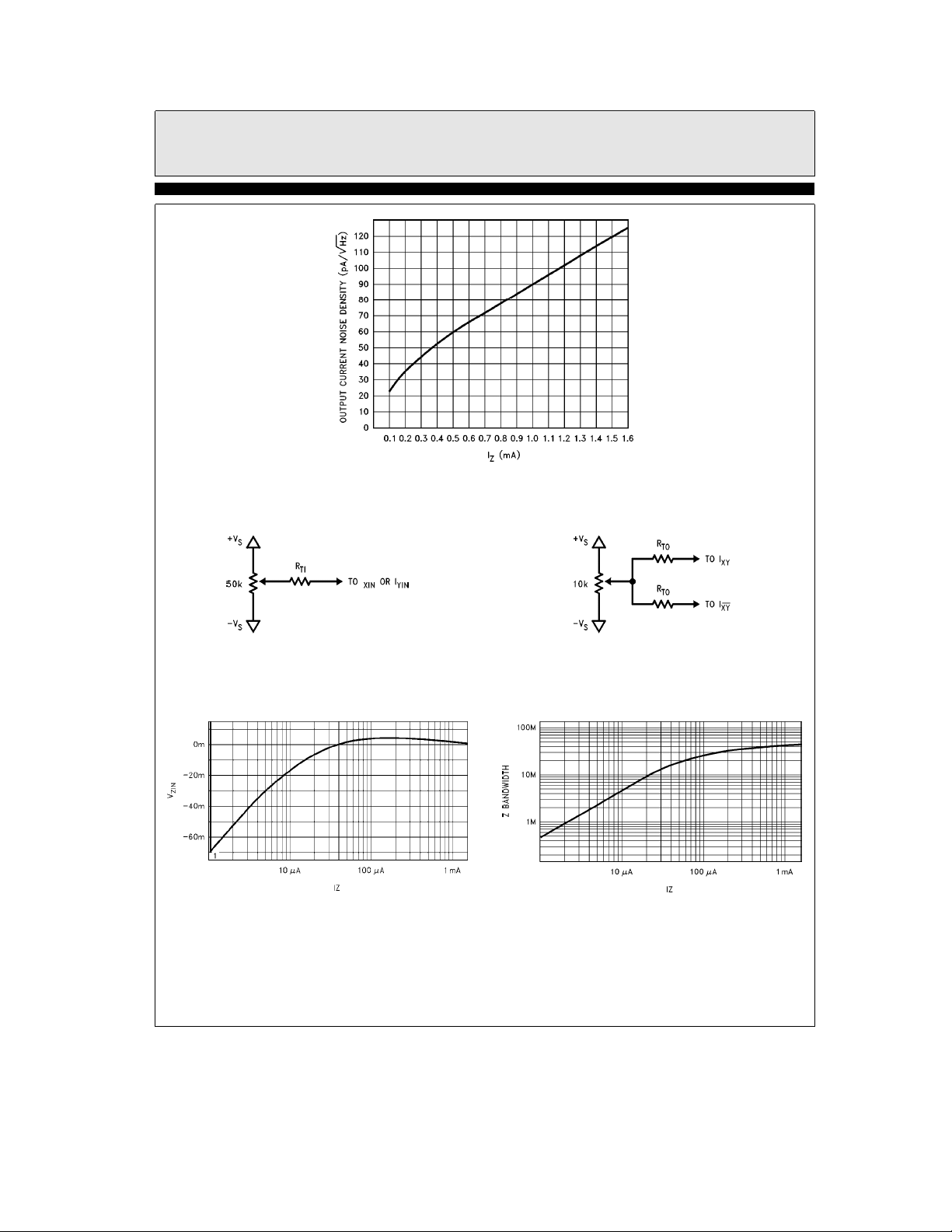
Figure 8. Output Noise Density vs IZBias
4083– 12
Input Offset Trim(s)
c
e
R
(V
TI
1.6 mA)/(16 mAcIZ)
S
4083– 13
e
R
(V
TO
Output Offset Trim
c
1.6 mA)/(30 mAcIZ)
S
4083– 14
Figure 9. Optional External Trim Networks
Figure 10. V
vs IZ(Typical)
ZIN
4083– 15
Figure 11. I
Bandwidth vs I
ZIN
4083– 16
Z
7
Page 8

EL4083C
Current Mode Four Quadrant Multiplier
General Operating Information
IZInput (Bias, Divisor) and Power
Supplies
The IZpin is a low impedance (k20X) virtual
ground current input. It can accept positive
current from a resistor connected to a positive
voltage source or the positive supply. The instantaneous bias for the multiplier gain core is proportional to this current value. Negative applied
current will put the multiplier portion of the circuit in a zero bias state and the voltage at the pin
will be clamped at a diode drop below ground.
The part will respond in a similar manner to currents from a current source such as the output of
a transconductance amplifier or one of its own
outputs. The overall transfer equation for the
EL4083 is:
c
K(I
X
As can be seen from the equation, the Z input can
serve as a divisor input. However, it is different
from the other two inputs in that the value of its
current determines the supply current of the part
and the bandwidth and compliance range of the
outputs and other two inputs. Table 1 gives the
equations describing these and other important
relationships. These dependencies can complicate
and/or limit the usefulness of this pin as a computational input. The I
pedance of the multiplying inputs can be particularly troublesome. See the I
Ý
RMS
2 circuit sections of the application note
for some ways of dealing with this.
Positive Supply Current I
Negative Supply Current I
Power Dissipation (See Figures 4 and 5) PWR
Multipling Input(s) Impedance R
Multiplying Input(s) Clip Point IX(clip)eIY(clip)eI
Multiplying Input(s) Full Scale Value I
Multiplying Input Resistor Values R
(In Terms of Peak Input Signal) R
Full Scale Output (Single Ended) I
Full Scale Output (Differential) (I
IZ(Bias) Input Voltage vs I
I
I
I
e
IY)/I
Signal Bandwidth vs I
Z
X,IY
X,IY
(IXY–IXY), KE1
Z
Signal Bandwidth vs I
1% Settling Time vs I
dependence of the im-
Z
divider and the
Z
Table 1. Basic Design Equations and Relationships
Z
Z
Z
Z
The primary intended use for the Z input is as a
programming pin similar in function to those on
programmable op amps. This enables one to
trade off power consumption against bandwidth
and settling time and allow the part to function
within its power dissipation rating over its full
operational supply range (
g
4.5V
b
g
16.5V).
The E4083 has been designed to function well for
I
values in the range of 200 mAkI
Z
which corresponds to I
and IYsignal band-
X
Z
k
1.6 mA
widths of about 50 MHz to over 200 MHz. Higher values of I
may cause problems at tempera-
Z
ture extremes while lower values down to zero
will progressively degrade the input referred D.C.
offsets and reduce speed. Below about 50 mAof
bias current the internal servo amplifier loop
which maintains the I
pin at ground will lose
Z
regulation and the voltage at the pin will start to
move negative (see Figure 10). This is accompanied by a significant increase in input impeddance of the pin. Figure 11 shows the A.C. bandwidth of the I
value of I
input as a function of the D.C.
Z
. Figures 6 and 7 show the bandwidth
Z
and 1% settling time of the multiplying inputs,
I
and I
X
, as functions of IZ.
Y
IXand IY(Multiplier) Inputs and Offset
Trimming
The IXand IYpins are low impedance (IZdependent) virtual ground current inputs that accept
bipolar signals. The input referred clip value is
equal to I
chosen to be 1.25
c
2 while the full scale value has been
Z
c
IZto maintain excellent distortion and linearity performance. Operating at
higher full scale values will degrade these two pa-
ae
3.4 mAaI
S
be
4.5 mAaI
S
e(a
e
R
ZX
ZY
(fs)eIY(fs)eI
X
e
VX(peak)/IX(fs)
X
e
VY(peak)/IY(fs)
Y
e
I
XY
XY
b
IXY)eIX(fs)cIY(fs)/I
XY
(See Figure 10)
(See Figure 11)
(See Figure 6)
(See Figure 7)
c
26
Z
c
27
Z
b(b
V
VS))c(4 mAaI
S
e
(32X)c1.6 mA/I
Z
c
1.25 (nominal)
Z
e
IX(fs)cIY(fs)/(I
c
26.5)
Z
Z
c
2
c
2)
Z
Z
8
Page 9

EL4083C
Current Mode Four Quadrant Multiplier
General Operating Information
Ð Contd.
rameters and, to some extent, bandwidth while
improving the signal to noise performance, feedthrough and control range.
The EL4083 is fundamentally different from conventional voltage mode multipliers in that the
available input range can be tailored to accommodate voltage sources of almost any size by selecting appropriate input series resistor values. If
desired, one can interface with voltages that are
much greater than the supplies from which the
part is powered. Current source signals can be
connected directly to the multiplier inputs. The
parts’ dynamic range can also be tailored to a
large extent for a current signal by the appropriate selection of I
manner as a virtual ground input of an operational amplifier and thus can serve as a summing
node for any number of voltage and/or current
signals. Outputs of components such as current
output DACs, transconductance amplifiers and
current conveyors can be directly connected to
the inputs.
Ideally, a multiplier should give zero output if
either one of its multiplying inputs is zero. A
nonzero output under these conditions is caused
by a combination of input and output referred
offsets. An output referred offset can be thought
of as a fixed value added to the output and thus
only affects D.C. accuracy. An input referred offset at a multiplying input allows signal to feedthrough from the other multiplying input to the
output(s). The EL4083 is trimmed during testing
at Elantec for X and Y input referred offset for I
e
1.6 mA. The internal trim networks provide a
current to each input which nulls the feedthrough caused by internal device mismatches.
These current values are ratioed to the value of
I
so that the input referred nulls are largely
Z
maintained at different values of I
there will be some mistracking in the trim networks so that the input referred null point will
deviate away from zero at values of I
1.6 mA. Figure 9 shows optional external input
and output referred offset trim networks which
can be used as needed to improve performance.
. These inputs act in the same
Z
. However,
Z
lower than
Z
As mentioned, the output referred offset only affects D.C. accuracy which may not be an issue in
A.C. applications. In gain control applications
one may only need to null feedthrough with respect to the gain control input.
In gain control (VCA) applications the X input
should be used as the control input and the signal
applied to the Y input since it has slightly higher
bandwidth and better linearity and distortion
performance.
Current Outputs (IXY,IXY), Feedthrough
and Distortion
Another unique feature of the EL4083 is the differential ground referenced current output structure. These outputs can drive 50X terminated
lines and reactive loads such as transformers, baluns, and LC tank and filter circuits directly.*
Unlike low impedance follower buffers, these outputs do not interact with the load to produce
ringing or instability. If a high level low impedance output is required, the outputs can be recovered differentially and converted to a single ended output with a fast op amp such as the EL2075
(see Figure 19). The outputs can also drive current input devices such as CMF amps, current
conveyors and its own inputs directly by simple
connection.
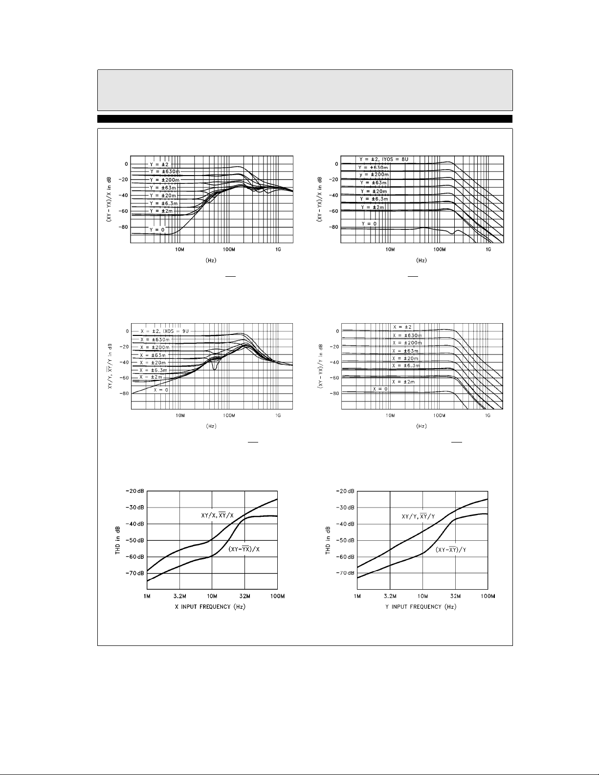
Figures 12 and 14 show the nulled gain and feedthrough characteristics of the I
puts which are virtually identical and differ only
in phase. Figure 12 is with the A.C. signal applied
to the X input with Y used as the gain control
and in Figure 14 these signals are reversed. Note
that in both cases the signal feedthrough rolls up
Z
and peaks near the cutoff frequency. This is quite
typical of the performance of all previous four
quadrant multipliers. Figures 13 and 15 show the
corresponding gain/feedthrough characteristics
for the differentially recovered output signal
I
XY-IXY
through at high frequencies is lower by more
than 40 dB.
* See EL2082 Data SheetÐReceiver IF Amplifier (Figure 19).
. Note that in this case the peak feed-
The EL2082 also has a current output.
XY
and IXYout-
9
Page 10

EL4083C
Current Mode Four Quadrant Multiplier
General Operating Information
Ð Contd.
Figures 16 and 17 show the total harmonic distortion for the single-ended and differential recovered outputs for a full scale A.C. input signal
on one input and a full scale D.C. control signal
on the other. Note that above about one megahertz to the cutoff frequency the THD of the differentially recovered signal is as much as 10 dB
lower than the single-ended signals.
10
Page 11
EL4083C
Current Mode Four Quadrant Multiplier
General Operating Information
Figure 12. Nulled IXYand IXYFrequency
Response (Signal on XIN,
Gain Controlled by YIN)
Ð Contd.
4083– 17
Figure 13. Nulled (IXY-IXY) Frequency Response
4083– 18
(Signal on XIN, Gain Controlled by YIN)
Figure 14. Nulled IXYand I
4083– 19
XY
Frequency Response (Signal
on YIN, Gain Controlled by XIN)
Figure 16. (Full Level XIN THD vs Frequency)
4083– 22
Figure 15. Nulled (IXY–IXY)
4083– 20
Frequency Response (Signal
on YIN, Gain Controlled by XIN)
4083– 21
Figure 17. (Full Level YIN THD vs Frequency)
11
Page 12
EL4083C
Current Mode Four Quadrant Multiplier
Applications
Basic Product Functions
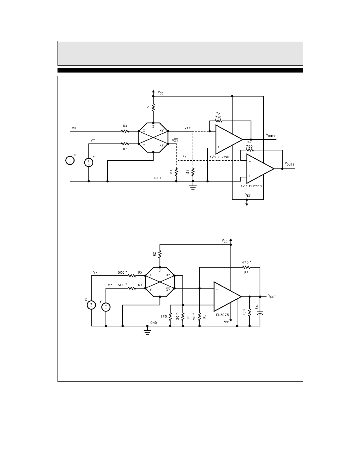
Figures 18 and 19 are the basic schematics for
many of the applications of the EL4083. These
can perform signal mixing, frequency doubling,
modulation, demodulation, gain control/voltagecontrolled amplification, multiplication and
squaring. Figure 18 has resistively terminated
differential outputs and has the widest bandwidth. The figure also shows the option of using
the EL2260 dual CMF amplifier to recover the
outputs differentially at very low impedance.
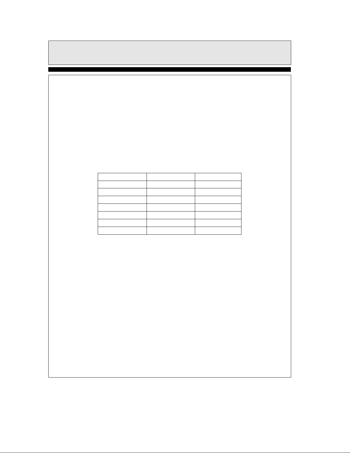
Table 2. Input Signal Assignments for Figures 18 and 19 Circuits
Application V
Mixer Signal 1 Signal 2
Frequency Doubler Signal Signal
Modulator Modulating Signal Carrier
Demodulator Local Oscillator Modulated Signal
Gain Control/VCA Gain Control Signal
Multiplier Signal 1 Signal 2
Squarer Signal Signal
*X means not connected if function is not used.
This has a maximum 3 dB bandwidth of
130 MHz and settles to 1% in 25 ns. Figure 19
uses an EL2075 at the outputs as a differential to
single ended converter with gain to take advantage of the performance enhancements of the differentially recovered output mentioned above
and to provide a high level low impedance drive.
b
The
3 dB bandwidth of this circuit is over
150 MHz using good layout techniques. However, to achieve this bandwidth one must restrict
the output swing to little more than 1 Vpp to
avoid running into the 500V/ms minimum slew
rate of the EL2075. Table 2 shows the input signal assignments for the applications listed above.
X
V
Y
12
Page 13
EL4083C
Current Mode Four Quadrant Multiplier
Applications
e
I
VCC/R
Z
R
X
R
Y
*1. 51X Resistors omitted when using EL2260
*2. Optimum value of RF determined by supplies and amount or tolerable peaking
b
3dBBWE90 MHz@V
(
Z
e
VX(MAX) / (1.25cIZ)
e
V
(MAX) / (1.25cIZ)
Y
Ð Contd.
e
S
g
5V, BWE150 MHz
@
g
15V)
Figure 18. Basic Schematic (Dual Diff Outs)
4083– 27
e
I
VCC/R
Z
R
X
R
Y
*Optimized for Wide Bandwidth
Z
e
VX(MAX) / (1.25cIZ)
e
VY(MAX) / (1.25cIZ)
4083– 28
Figure 19. Basic Schematic (Single Ended Converted)
(150 MHz VCA)
13
Page 14

EL4083C
Current Mode Four Quadrant Multiplier
Other Applications
Elantec has also published an applications note
covering other applications of the EL4083. These
include dividers, squaring and square rooting circuits, several RMS and power measurement circuits, and a wideband AGC circuit. Also presented are two polynomial computation examples for
video and some HDTV quality fader and summing circuits. The EL4083 has been found flexible enough to easily implement all of the classic
four quadrant multiplier applications and also offer interesting new applications possibilities.
EL4083 Macromodel
This macromodel is compatible with PSPICE
(copywritten by Microsim Corporation) . It has
been designed to work accurately for fixed values
of I
(bias) in the range of 200 mA to 1.6 mA. The
Z
additional simulation burden imposed by including provision for a time varying I
not worthwhile. The value of I
was thought
Z
is specified to
Z
the model by the parameter NS. The relation be-
Macromodel
*EL4083 Macromodel
*Revision A, August 22, 1994
*
*Connection: IZ(BIAS)
*
*
*
*
*
*
*
.subckt EL4083 ZIN XIN YIN VEE VCC IXY IYX
.MODEL M1MP5DIODE D TT
VJ
.MODEL M2MDCAP D TT
VJ
.MODEL M3MNPN1 NPN CJC
BF
.MODEL M4MPNP1 PNP CJC
IS
C1 N9 N7 9p
C2 N7 0 350f
C3 N19 N16 9p
C4 N16 0 350f
IX(in)
l
IY(in)
ll
VEE
lll
llll
lllll
llllll
VCC
IXY
/IXY
lllllll
e
600m XTIe3EGe1.11 RSe80m
e
800m RSe300
e
120 CJSe480f
e
1f BFe90 CJSe480f
e
60p ISe1f CJOe300f
e
100n ISe2e-17 CJOe1p
e
1.3p TFe120p ISe1.04f
e
1.79p TFe50.166666666667p
tween I
and NS is; I
Z
e
200 mAcNS. All other
Z
inputs can accept time varying signals.
The model will provide good transient and frequency response and settling time estimates as
well as time domain switching results. Input and
output impedance and overload responses are
correctly modeled. The D.C. current drawn from
supplies for a given value of I
is also correct.
Z
Noise, PSRR and the temperature dependence of
A.C. parameters such as frequency response and
settling time are not modeled. Linearity and distortion results from the model will be worse than
the real part by about a factor of three and do not
show the correct frequency dependence.
The macromodel is constructed from simple controlled sources, passive components and stripped
transistor and diode models. As such it should be
usable, perhaps with slight modification, on all
but student or demonstration simulators where
the model’s size may be a problem.
D1 0 N15 M2MDCAP 12
D10 0 N26 M1MP5DIODE 1
D11 N26 N27 M1MP5DIODE 1
D12 N29 N30 M1MP5DIODE 1
D13 0 N31 M1MP5DIODE 1
D14 VBP N34 M1MP5DIODE 2
D15 N34 VBP M1MP5DIODE 2
D16 0 N34 M2MDCAP 12.5
D17 N35 0 M2MDCAP 12.5
D18 N35 VBN M1MP5DIODE 2
D19 VBN N35 M1MP5DIODE 2
D2 N15 0 M2MDCAP 12
D20 N42 N10 M2MDCAP 4
D21 N10 0 M2MDCAP 4
D22 0 N20 M2MDCAP 4
D23 N20 N45 M2MDCAP 4
D3 0 N12 M1MP5DIODE 8
D4 N55 N13 M1MP5DIODE 8
D5 0 N25 M2MDCAP 6
D6 N25 0 M2MDECAP 6
D7 0 N22 M1MP5DIODE 8
D8 N54 N23 M1MP5DIODE 8
D9 0 N28 M1MP5DIODE 1
EV94 0 VBN 0 N45 1
14
Page 15

EL4083C
Current Mode Four Quadrant Multiplier
Macromodel
EV95 VBP 0 N42 0 1
EV96 N54 0 N21 0 650m
EV97 N55 0 N11 0 650m
EV98 N27 0 N28 0 1
EV99 N29 0 SWIN 0 1
FI10 VN-VEE VFI10 1
FI11 VCC VP-VFI11 1
FI12 VCC N39 VFI12 1
FI13 N37 VEE VFI13 1
FI14 VCC N38 VFI14 1
FI15 N36 VEE VFI15 1
FI16 N45 VEE VFI16 1
FI17 VCC N42 VFI17 1
FI18 N37 N36 VFI18 500m
FI19 N38 N39 VFI19 500m
aVNb
FI20 VN
aVPb
FI21 VP
FI22 0 N21 VFI22 1
FI23 N21 0 VFI23 1
FI24 N24 0 VFI24 2
FI25 N14 0 VFI25 2
FI26 N11 0 VFI26 1
FI27 0 N11 VFI27 1
FI28 VCC VEE VFI28 21
FI 29 N28 ZB1 VFI29 1
FI5 N33 0 VFI5 1
FI6 0 N33 VFI6 1
FI7 N35 N34 VFI7 1
a
FI8 VN
FI9 VCC VP
IIBGN 0 VEE 2.2m
IIBGP VCC 0 2.46m
IIISWB N32 VEE 629u
IIISWI SWIN VEE 555u
IIZSU N28 VEE 10u
L1 N7 IXA 71n
L2 XIN N7 4n
L3 N16 IYA 71n
L4 YIN N16 4n
L5 N46 IYX 4n
L6 N47 IXY 4n
Q10 N10 VP
Q10 N46 VN
Q11 N47 VN
Q12 N46 VN
Q13 0 N34 N56[VEE]M4MPNP1 400m
Q14 0 N34 N57[VEE]M4MPNP1 400m
Q15 0 N35 N58[VEE]M3MNPN1 400m
Q16 0 N35 N59[VEE]M3MNPN1 400m
Q2 0 N10 VP
Q3 0 N20 VN
VEE VFI8 1
a
a
a
a
b
b
a
Ð Contd.
VFI20 500m
VFI21 500m
VFI9 1
[
VEE]M4MPNP1 2
N36[VEE]M3MNPN1 2
N37[VEE]M3MNPN1 2
N37[VEE]M3MNPN1 2
[
VEE]M4MPNP1 2
[
VEE]M3MNPN1 2
b
Q4 0 N20 VN
Q5 N46 VP
Q6 N47 VP
Q7 N46 VP
Q8 N47 VP
Q9 N47 VN
R1 N15 N7 60 TC
R10 N16 N17 450 TC
R11 YIN N16 100 TC
R12 0 SWIN 500 TC
R13 N56 N38 35 TC
R14 N57 N39 35 TC
R15 N37 N58 35 TC
R16 N36 N59 35 TC
R17 N46 IYX 100 TC
R18 N47 IXY 100 TC
R2 N11 IXC 6.25 TC
R3 N9 IXC 4.5 TC
R4 N7 IXA 1.5K TC
R5 XIN N7 100 TC
R6 N25 N16 156 TC
R7 N21 IYC 6.25 TC
R8 ITC N19 45 TC
R9 N17 IYA 45 TC
RSU VEE 0 16K TC
VFI10 N43 N44 0.0
VFI11 N40 N41 0.0
VFI12 ZB4 ZB5 0.0
VFI13 ZB5 ZB6 0.0
VFI14 ZB3 ZB4 0.0
VFI15 ZB6 ZB7 0.0
VFI16 N44 ZB9 0.0
VFI17 N41 ZB8 0.0
VFI18 IYB IYC 0.0
VFI19 IYA IYB 0.0
VFI20 IXB IXC 0.0
VFI21 IXA IXB 0.0
VFI22 N22 N24 0.0
VFI23 N23 N24 0.0
VFI24 ZB2 ZB3 0.0
VFI25 ZB1 ZB2 0.0
VFI26 N13 N14 0.0
VF127 N12 N14 0.0
VFI28 ZB9 VEE 0.0
VFI29 ZIN N26 0.0
VF15 N30 N32 0.0
VFI6 N31 N32 0.0
VFI7 N33 0 0.0
VFI8 ZB8 N43 0.0
VFI9 ZB7 N40 0.0
.ENDS
[
VEE]M3MNPN1 2
b
N39[VEE]M4MPNP1 2
a
N39[VEE]M4MPNP1 2
a
N38[VEE]M4MPNP1 2
b
N38[VEE]M4MPNP1 2
b
N36[VEE]M3MNPN1 2
e
e
e
824u 7.67u
e
00
e
00
e
824u 7.67u
e
00
e
00
e
00
e
00
e
00
e
00
e
00
00
e
00
e
00
e
824u 7.67u
e
00
00
e
00
e
00
15
Page 16

EL4083C
Current Mode Four Quadrant Multiplier
EL4083CDecember 1995 Rev B
General Disclaimer
Specifications contained in this data sheet are in effect as of the publication date shown. Elantec, Inc. reserves the right to make changes
in the circuitry or specifications contained herein at any time without notice. Elantec, Inc. assumes no responsibility for the use of any
circuits described herein and makes no representations that they are free from patent infringement.
WARNING Ð Life Support Policy
Elantec, Inc. products are not authorized for and should not be
used within Life Support Systems without the specific written
consent of Elantec, Inc. Life Support systems are equipment in-
Elantec, Inc.
1996 Tarob Court
Milpitas, CA 95035
Telephone: (408) 945-1323
(800) 333-6314
Fax: (408) 945-9305
European Office: 44-71-482-4596
tended to support or sustain life and whose failure to perform
when properly used in accordance with instructions provided can
be reasonably expected to result in significant personal injury or
death. Users contemplating application of Elantec, Inc. products
in Life Support Systems are requested to contact Elantec, Inc.
factory headquarters to establish suitable terms & conditions for
these applications. Elantec, Inc.’s warranty is limited to replacement of defective components and does not cover injury to persons or property or other consequential damages.
Printed in U.S.A.16
 Loading...