

Page 1
EL2250C, EL2450C
125MHz Single Supply Dual/Quad Op Amps
EL2250C, EL2450C
Features
• Specified for +3V, +5V, or ±5V
applications
• Large input common mode range
0V < VCM < VS -1.2V
• Output swings to ground without
saturating
• -3dB bandwidth = 125MHz
• ± 0.1dB bandwidth = 30MHz
• Low supply current = 5mA (per
amplifier)
• Slew rate = 275V/µs
• Low offset voltage = 4mV max
• Output current = ±100mA
• High open loop gain = 80dB
• Differential gain = 0.05%
• Differential phase = 0.05°
Applications
• Video amplifiers
• PCMCIA applications
• A/D drivers
• Line drivers
• Portable computers
• High speed communications
• RGB printers, FAX, scanners
• Broadcast equipment
• Active filtering
Ordering Information
Part No Package Tape & Reel Outline #
EL2250CN 8-Pin PDIP - MDP0031
EL2250CS 8-Pin SO - MDP0027
EL2250CS-T7 8-Pin SO 7” MDP0027
EL2250CS-T13 8-Pin SO 13” MDP0027
EL2450CN 14-Pin PDIP - MDP0031
EL2450CS 14-Pin SO - MDP0027
EL2450CS-T7 14-Pin SO 7” MDP0027
EL2450CS-T13 14-Pin SO 13” MDP0027
General Description
The EL2250C/EL2450C are part of a family of the electronics industries fastest single supply op amps available. Prior single supply op
amps have generally been limited to bandwidths and slew rates to that
of the EL2250C/EL2450C. The 125MHz bandwidth, 275V/µs slew
rate, and 0.05%/0.05° differential gain/differential phase makes this
part ideal for single or dual supply video speed applications. With its
voltage feedback architecture, this amplifier can accept reactive feedback networks, allowing them to be used in analog filtering
applications. The inputs can sense signals below the bottom supply
rail and as high as 1.2V below the top rail. Connecting the load resistor
to ground and operating from a single supply, the outputs swing completely to ground without saturating. The outputs can also drive to
within 1.2V of the top rail. The EL2250C/EL2450C will output
±100mA and will operate with single supply voltages as low as 2.7V,
making them ideal for portable, low power applications.
The EL2250C/EL2450C are available in PDIP and SO packages in
industry standard pin outs. Both parts operate over the industrial temperature range of -40°C to +85°C, and are part of a family of single
supply op amps. For single amplifier applications, see the
EL2150C/EL2157C. For dual and triple amplifiers with power down
and output voltage clamps, see the EL2257C/EL2357C.
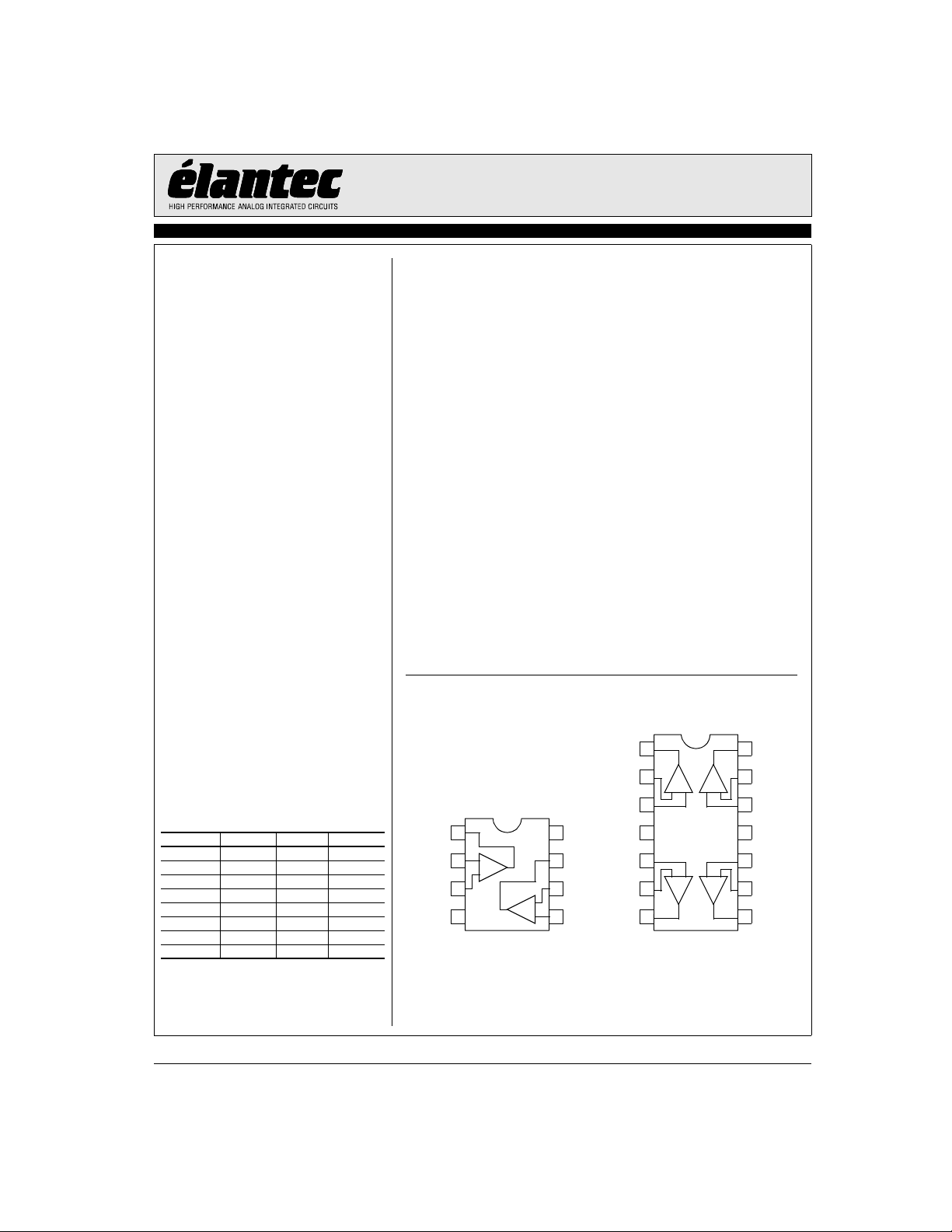
Connection Diagrams
1
OUTA
2
INA-
3
INA+
4
GND
(8-Pin SO & 8-Pin PDIP)
-
A
+
EL2250C
1
OUTA
2
INA-
INA+
8
VS+
7
OUTB
6
INB-
-
B
5
+
INB+
VS+
INB+
INB-
OUTB
A D
- + -+
3
4
5
- + -+
6
B C
7
EL2450C
(14-Pin SO & 14-Pin PDIP)
14
OUTD
13
IND-
12
IND+
11
GND
10
INC+
9
INC-
8
OUTC
September 26, 2001
Note: All information contained in this data sheet has been carefully checked and is believed to be accurate as of the date of publication; however, this data sheet cannot be a “controlled document”. Current revisions, if any, to these
specifications are maintained at the factory and are available upon your request. We recommend checking the revision level before finalization of your design documentation.
© 2001 Elantec Semiconductor, Inc.
Page 2
EL2250C, EL2450C
125MHz Single Supply Dual/Quad Op Amps
Absolute Maximum Ratings (T
Supply Voltage between VS and GND +12.6V
Input Voltage (IN+, IN-) GND-0.3V,VS+0.3V
EL2250C, EL2450C
Differential Input Voltage ±6V
Maximum Output Current 90mA
= 25°C)
A
Power Dissipation See Curves
Storage Temperature Range -65°C to +150°C
Ambient Operating Temperature Range -40°C to +85°C
Operating Junction Temperature 150°C
Output Short Circuit Duration (Note 1)
Important Note:
All parameters having Min/Max specifications are guaranteed. Typ values are for information purposes only. Unless otherwise noted, all tests are at the
specified temperature and are pulsed tests, therefore: TJ = TC = TA.
DC Electrical Characteristics
VS = +5V, GND = 0V, TA = 25°C, V
Parameter Description Test Conditions Min Typ Max Unit
V
OS
TCV
Offset Voltage EL2250C -2 2 mV
Offset Voltage Temperature Coefficient Measured from T
OS
IB Input Bias Current V
I
OS
TCI
Input Offset Current V
Input Bias Current Temperature Coefficient Measured from T
OS
PSRR Power Supply Rejection Ratio VS = +2.7V to +12V 55 70 dB
CMRR Common Mode Rejection Ratio VCM = 0V to +3.8V 55 65 dB
CMIR Common Mode Input Range 0 VS-1.2 V
R
IN
C
IN
R
OUT
I
S
Input Resistance Common Mode 1 2 MΩ
Input Capacitance SO Package 1 pF
Output Resistance A
Supply Current (per amplifier) VS = +12V 5 6.5 mA
PSOR Power Supply Operating Range 2.7 12.0 V
CM
= 1.5V, V
= 1.5V, unless otherwise specified.
OUT
EL2450C -4 4 mV
= 0V -5.5 -10 µA
IN
= 0V -750 150 750 nA
IN
VCM = 0V to +3.0V 55 70 dB
PDIP Package 1.5 pF
= +1 40 mΩ
V
MIN
MIN
to T
to T
MAX
MAX
10 µV/°C
50 nA/°C
DC Electrical Characteristics
VS = +5V, GND = 0V, TA = 25°C, V
Parameter Description Test Conditions Min Typ Max Unit
AVOL Open Loop Gain VS = +12V, V
V
OP
Positive Output
Voltage Swing
= +1.5V, V
CM
= +1.5V, unless otherwise specified.
OUT
to GND
V
= +1.5V to +3.5V, R
OUT
V
= +1.5V to +3.5V, R
OUT
GND
VS = +12V, AV = +1, R
VS = +12V, AV = +1, R
VS = ±5V, AV = +1, R
VS = ±5V, AV = +1, R
VS = +3V, AV = +1, R
2
= +2V to +9V, R
OUT
L
L
= 1kΩ to 0V 4.0 V
L
= 150Ω to 0V 3.4 3.8 V
L
= 150Ω to 0V 1.8 1.95 V
L
= 1kΩ
L
= 1kΩ to GND 70 dB
L
= 150Ω to
L
60 80 dB
60 dB
= 1kΩ to 0V 10.8 V
= 150Ω to 0V 9.6 10.0 V
Page 3
EL2250C, EL2450C
125MHz Single Supply Dual/Quad Op Amps
DC Electrical Characteristics
VS = +5V, GND = 0V, TA = 25°C, V
Parameter Description Test Conditions Min Typ Max Unit
V
ON
Negative Output
Voltage Swing
I
OUT
Output Current
1. Internal short circuit protection circuitry has been built into the EL2250C/EL2450C; see the Applications section
= +1.5V, V
CM
[1]
= +1.5V, unless otherwise specified.
OUT
VS = +12V, AV = +1, R
V S= ±5V, AV = +1, R
VS = ±5V, AV = +1, R
VS = ±5V, AV = +1, R
VS = ±5V, AV = +1, R
mA
= 150Ω to 0V 5.5 8 mV
L
= 1kΩ to 0V -4.0 V
L
= 150Ω to 0V -3.7 -3.4 V
L
= 10Ω to 0V ±75 ±100 mA
L
= 50Ω to 0V±60V
L
EL2250C, EL2450C
Closed Loop AC Electrical Characteristics
VS = +5V, GND = 0V, TA = 25°C, V
= +1.5V, V
CM
= +1.5V, AV = +1, R
OUT
= 0Ω, RL = 150Ω to GND pin, unless otherwise specified.
F
[1]
Parameter Description Test Conditions Min Typ Max Unit
BW -3dB Bandwidth
(V
=400mVp-p)
OUT
BW ±0.1dB Bandwidth
(V
=400mVp-p)
OUT
VS = +5V, AV = +1, R
VS = +5V, AV = -1, R
VS = +5V, AV = +2, R
VS = +5V, AV = +10, R
VS = +12V, AV = +1, R
VS = +3V, AV = +1, R
VS = +12V, AV = +1, R
VS = +5V, AV = +1, R
VS = +3V, AV = +1, R
= 0Ω 125 MHz
F
= 500Ω 60 MHz
F
= 500Ω 60 MHz
F
= 500Ω 6 MHz
F
= 0Ω 150 MHz
F
= 0Ω 100 MHz
F
= 0Ω 25 MHz
F
= 0Ω 30 MHz
F
= 0Ω 20 MHz
F
GBWP Gain Bandwidth Product VS = +12V, @ AV = +10 60 MHz
PM Phase Margin R
SR Slew Rate VS = +10V, R
tR, t
F
Rise Time, Fall Time ±0.1V Step 2.8 ns
= 1kΩ, C
L
VS = +5V, R
= 6pF 55 °
L
= 150Ω, V
L
= 150Ω, V
L
= 0V to +6V 200 275 V/µs
OUT
= 0V to +3V 300 V/µs
OUT
OS Overshoot ±0.1V Step 10 %
t
PD
t
S
dG Differential Gain
dP Differential Phase
e
N
i
N
Propagation Delay ±0.1V Step 3.2 ns
0.1% Settling Time VS = ±5V, R
0.01% Settling Time VS = ±5V, R
[2]
[2]
±3V
±3V
AV = +2, R
AV = +2, R
= 500Ω, A
L
= 500Ω, A
L
= 1kΩ 0.05 %
F
= 1kΩ 0.05 °
F
= +1, V
V
= +1, V
V
OUT
OUT
=
=
40 ns
75 ns
Input Noise Voltage f = 10kHz 48 nV/√Hz
Input Noise Current f = 10kHz 1.25 pA/√Hz
1. All AC tests are performed on a “warmed up” part, except slew rate, which is pulse tested
2. Standard NTSC signal = 286mV
, f = 3.58MHz, as VIN is swept from 0.6V to 1.314V; RL is DC coupled
P-P
3
Page 4
EL2250C, EL2450C
125MHz Single Supply Dual/Quad Op Amps
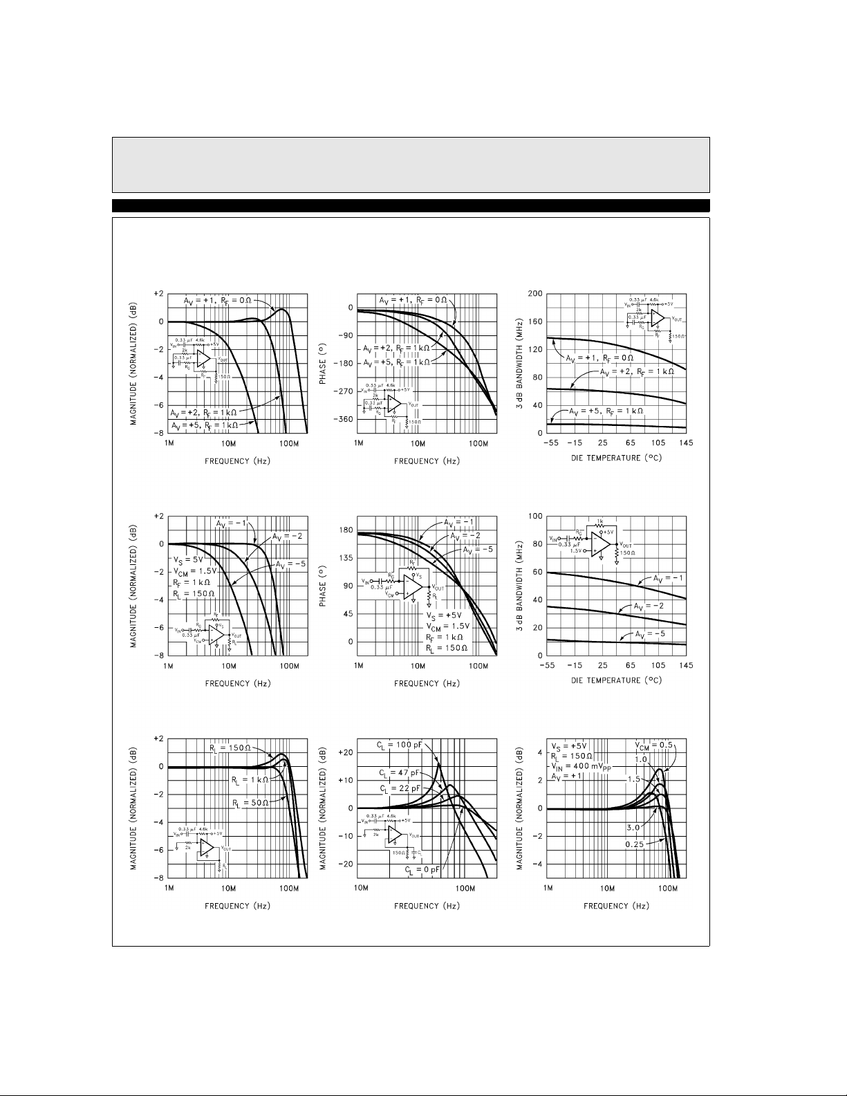
Typical Performance Curves
EL2250C, EL2450C
Non-Inverting Frequency Response
(Gain)
Non-Inverting Frequency Response
(Phase)
Inverting Frequency Response (Phase)Inverting Frequency Response (Gain)
3dB Bandwidth vs Temperature for NonInverting Gains
3dB Bandwidth vs Temperature for
Inverting Gains
Frequency Response for Various R
L
Frequency Response for Various C
4
L
Non-Inverting Frequency Response vs
Common Mode Voltage
Page 5
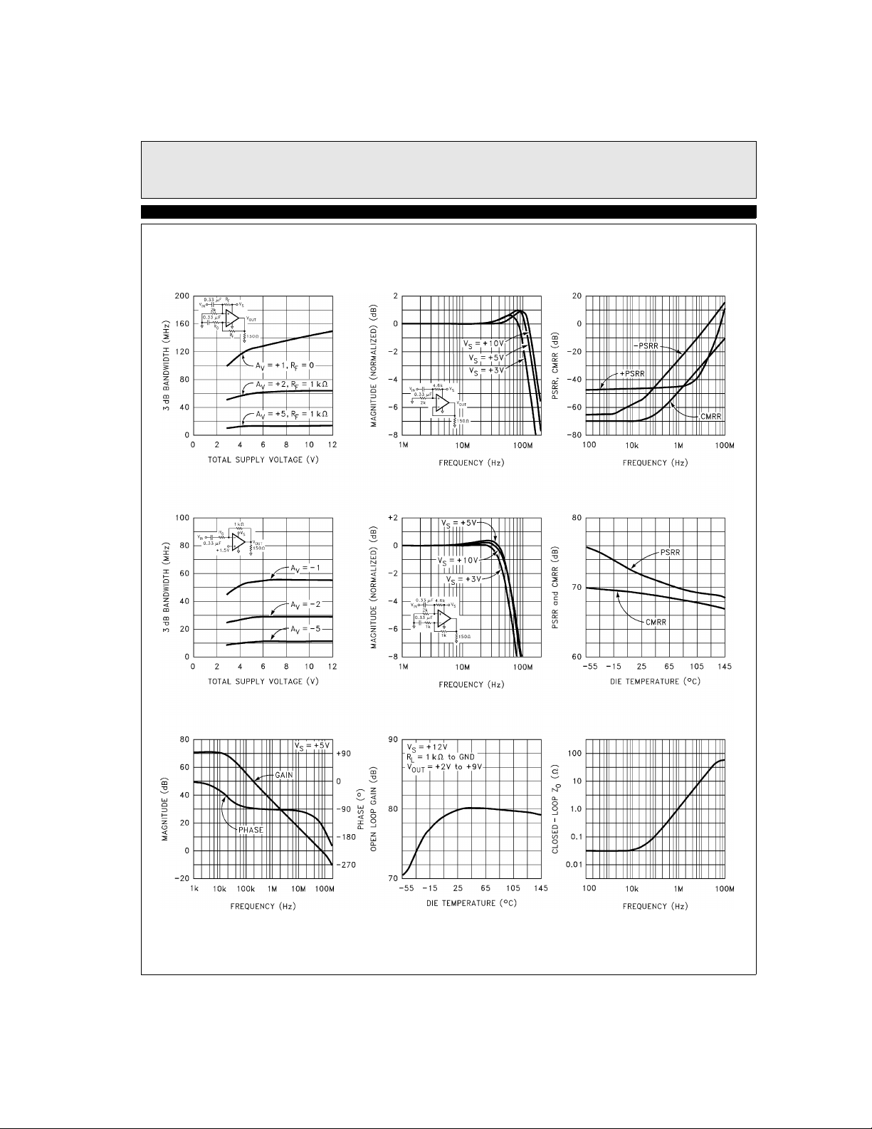
EL2250C, EL2450C
125MHz Single Supply Dual/Quad Op Amps
EL2250C, EL2450C
3dB Bandwidth vs Supply Voltage for
Non-Inverting Gains
3dB Bandwidth vs Supply Voltage for
Inverting Gains
Frequency Response for Various Supply
Voltages, AV = + 1
Voltages, AV = + 2
PSSR and CMRR vs Frequency
PSRR and CMRR vs Die TemperatureFrequency Response for Various Supply
Open Loop Gain and Phase vs Frequency Open Loop Voltage Gain vs Die
Temperature
5
Closed Loop Output Impedance vs
Frequency
Page 6
EL2250C, EL2450C
125MHz Single Supply Dual/Quad Op Amps
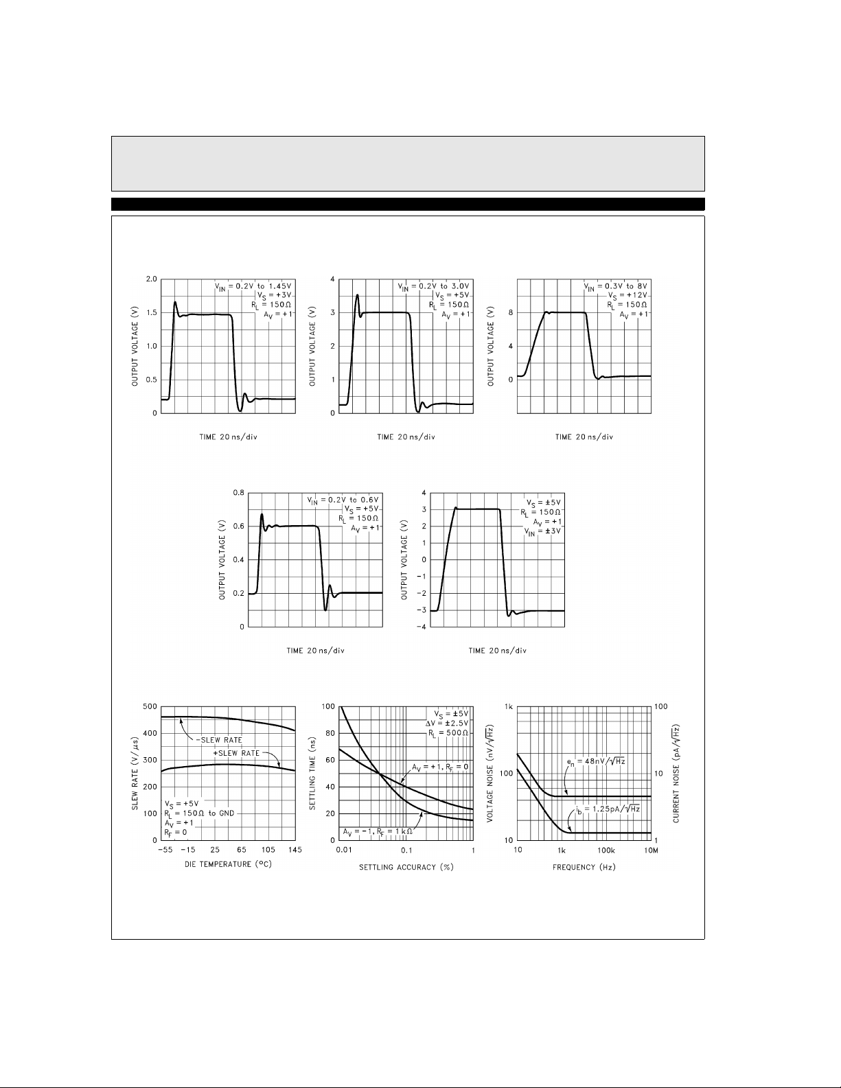
Large Signal Step Response, VS = +3V Large Signal Step Response, VS = +5V Large Signal Step Response, VS = +12V
EL2250C, EL2450C
Small Signal Step Response Large Signal Step Response, VS = ±5V
Slew Rate vs Temperature Settling Time vs Settling Accuracy Voltage and Current Noise vs Frequency
6
Page 7

EL2250C, EL2450C
125MHz Single Supply Dual/Quad Op Amps
EL2250C, EL2450C
Differential Gain for
Single Supply Operation
2nd and 3rd Harmonic Distortion vs
Frequency
Differential Phase for
Single Supply Operation
2nd and 3rd Harmonic Distortion vs
Frequency
Differential Gain and Phase
for Dual Supply Operation
2nd and 3rd Harmonic Distortion vs
Frequency
Output Voltage Swing vs Frequency for
THD < 0.1%
Output Voltage Swing vs Frequency for
Unlimited Distortion
7
Output Current vs Die Temperature
Page 8

EL2250C, EL2450C
125MHz Single Supply Dual/Quad Op Amps
EL2250C, EL2450C
Supply Current vs Supply Voltage (per
amplifier)
Offset Voltage vs Die Temperature (4
Samples)
Supply Current vs Die Temperature (per
amplifier)
Input Bias Current vs Input Voltage
Input Resistance vs Die Temperature
Input Offset Current and Input Bias
Current vs Die Temperature
Positive Output Voltage Swing vs Die
Temperature, RL = 150Ω to GND
Negative Output Voltage Swing vs Die
Temperature, RL = 150Ω to GND
8
Channel to Channel Isolation vs
Frequency
Page 9

EL2250C, EL2450C
125MHz Single Supply Dual/Quad Op Amps
EL2250C, EL2450C
Package Power Dissipation vs Ambient Temp.
SEMI G42-88 Single Layer Test Board
1.8
1.54W
1.6
1.4
1.25W
1.2
1
0.8
0.6
Power Dissipation (W)
0.4
0.2
0
0 25 50 75 100 125 15085
P
D
I
P
1
4
θ
J
A
=
P
D
8
I
P
8
θ
J
A
=
1
0
0
°
C
/
W
Ambient Temperature (°C)
Simplified Schematic
Package Power Dissipation vs Ambient Temp.
JEDEC JESD51-3 Low Effective Thermal Conductivity Test Board
1.2
1.042W
1
781W
1
°
C
/
W
0.8
0.6
0.4
Power Dissipation (W)
0.2
0
0 25 50 75 100 125 15085
S
O
1
4
θ
J
A
=
1
2
0
°
S
O
8
θ
C
J
A
=
1
6
0
°
C
/
W
Ambient Temperature (°C)
/
W
9
Page 10

EL2250C, EL2450C
125MHz Single Supply Dual/Quad Op Amps
Applications Information
Product Description
EL2250C, EL2450C
The EL2250C/EL2450C are part of a family of the
industries fastest single supply operational amplifiers.
Connected in voltage follower mode, their -3dB bandwidth is 125MHz while maintaining a 275 V/µs slew
rate. With an input and output common mode range that
includes ground, these amplifiers were optimized for
single supply operation, but will also accept dual supplies. They operate on a total supply voltage range as
low as +2.7V or up to +12V. This makes them ideal for
+3V applications, especially portable computers.
While many amplifiers claim to operate on a single supply, and some can sense ground at their inputs, most fail
to truly drive their outputs to ground. If they do succeed
in driving to ground, the amplifier often saturates, causing distortion and recovery delays. However, special
circuitry built into the EL2250C/EL2450C allows the
output to follow the input signal to ground without
recovery delays.
Power Supply Bypassing And Printed Circuit
Board Layout
As with any high-frequency device, good printed circuit
board layout is necessary for optimum performance.
Ground plane construction is highly recommended.
Lead lengths should be as short as possible. The power
supply pins must be well bypassed to reduce the risk of
oscillation. The combination of a 4.7µF tantalum capacitor in parallel with a 0.1 µF ceramic capacitor has been
shown to work well when placed at each supply pin. For
single supply operation, where the GND pin is connected to the ground plane, a single 4.7µF tantalum
capacitor in parallel with a 0.1µF ceramic capacitor
across the VS+ and GND pins will suffice.
For good AC performance, parasitic capacitance should
be kept to a minimum. Ground plane construction
should be used. Carbon or Metal-Film resistors are
acceptable with the Metal-Film resistors giving slightly
less peaking and bandwidth because of their additional
series inductance. Use of sockets, particularly for the SO
package should be avoided if possible. Sockets add parasitic inductance and capacitance which will result in
some additional peaking and overshoot.
Supply Voltage Range and Single-Supply
Operation
The EL2250C/EL2450C have been designed to operate
with supply voltages having a span of greater than 2.7V,
and less than 12V. In practical terms, this means that the
EL2250C/EL2450C will operate on dual supplies ranging from ±1.35V to ±6V. With a single-supply, the
EL2250C/EL2450C will operate from +2.7V to +12V.
Performance has been optimized for a single +5V
supply.
Pins 8 and 4 are the power supply pins on the EL2250C.
The positive power supply is connected to pin 8. When
used in single supply mode, pin 4 is connected to
ground. When used in dual supply mode, the negative
power supply is connected to pin 4.
Pins 4 and 11 are the power supply pins on the
EL2450C. The positive power supply is connected to pin
4. When used in single supply mode, pin 11 is connected
to ground. When used in dual supply mode, the negative
power supply is connected to pin 11.
As supply voltages continue to decrease, it becomes necessary to provide input and output voltage ranges that
can get as close as possible to the supply voltages. The
EL2250C/EL2450C have an input voltage range that
includes the negative supply and extends to within 1.2V
of the positive supply. So, for example, on a single +5V
supply, the EL2250C/EL2450C have an input range
which spans from 0V to 3.8V.
The output range of the EL2250C/EL2450C is also quite
large. It includes the negative rail, and extends to within
1V of the top supply rail with a 1kΩ load. On a +5V sup-
ply, the output is therefore capable of swinging from 0V
to +4V. On split supplies, the output will swing ±4V. If
the load resistor is tied to the negative rail and split supplies are used, the output range is extended to the
negative rail.
Choice Of Feedback Resistor, R
The feedback resistor forms a pole with the input capacitance. As this pole becomes larger, phase margin is
reduced. This increases ringing in the time domain and
peaking in the frequency domain. Therefore, RF has
F
10
Page 11

EL2250C, EL2450C
125MHz Single Supply Dual/Quad Op Amps
EL2250C, EL2450C
some maximum value which should not be exceeded for
optimum performance. If a large value of RF must be
used, a small capacitor in the few picofarad range in parallel with RF can help to reduce this ringing and peaking
at the expense of reducing the bandwidth.
As far as the output stage of the amplifier is concerned,
RF + RG appear in parallel with RL for gains other than
+1. As this combination gets smaller, the bandwidth
falls off. Consequently, RF has a minimum value that
should not be exceeded for optimum performance.
For AV = +1, R
(noise gain of 2), optimum response is obtained with R
between 500Ω and 1kΩ. For Av = -4 or +5 (noise gain of
5), keep R
= 0Ω is optimum. For A
F
between 2kΩ and 10kΩ.
F
= -1 or +2
V
Video Performance
For good video performance, an amplifier is required to
maintain the same output impedance and the same frequency response as DC levels are changed at the output.
This can be difficult when driving a standard video load
of 150Ω, because of the change in output current with
DC level. Differential Gain and Differential Phase for
the EL2250C/EL2450C are specified with the black
level of the output video signal set to +1.2V. This allows
ample room for the sync pulse even in a gain of +2 configuration. This results in dG and dP specifications of
0.05% and 0.05° while driving 150Ω at a gain of +2.
Setting the black level to other values, although acceptable, will compromise peak performance. For example,
looking at the single supply dG and dP curves for
R
=150Ω, if the output black level clamp is reduced
L
from 1.2V to 0.6V dG/dP will increase from
0.05%/0.05° to 0.08%/0.25° Note that in a gain of +2
configuration, this is the lowest black level allowed such
that the sync tip doesn’t go below 0V.
If your application requires that the output goes to
ground, then the output stage of the EL2250C/EL2450C,
like all other single supply op amps, requires an external
pull down resistor tied to ground. As mentioned above,
the current flowing through this resistor becomes the DC
bias current for the output stage NPN transistor. As this
current approaches zero, the NPN turns off, and dG and
dP will increase. This becomes more critical as the load
resistor is increased in value. While driving a light load,
such as 1kΩ, if the input black level is kept above 1.25V,
dG and dP are a respectable 0.03% and 0.03°.
For other biasing conditions see the Differential Gain
and Differential Phase vs. Input Voltage curves.
Output Drive Capability
In spite of their moderately low 5mA of supply current,
the EL2250C/EL2450C are capable of providing
±100mA of output current into a 10Ω load, or ±60mA
F
into 50Ω. With this large output current capability, a
50Ω load can be driven to ±3V with V
it an excellent choice for driving isolation transformers
in telecommunications applications.
= ±5V, making
S
Driving Cables and Capacitive Loads
When used as a cable driver, double termination is
always recommended for reflection-free performance.
For those applications, the back-termination series resistor will de-couple the EL2250C/EL2450C from the
cable and allow extensive capacitive drive. However,
other applications may have high capacitive loads without a back-termination resistor. In these applications, a
small series resistor (usually between 5 Ω and 50 Ω) can
be placed in series with the output to eliminate most
peaking. The gain resistor (RG) can then be chosen to
make up for any gain loss which may be created by this
additional resistor at the output.
Video Sync Pulse Remover Application
All CMOS Analog to Digital Converters (A/Ds) have a
parasitic latch-up problem when subjected to negative
input voltage levels. Since the sync tip contains no useful video information and it is a negative going pulse, we
can chop it off.
Figure 1 shows a unity gain connected amplifier A of an
EL2250C. Figure 2 shows the complete input video signal applied at the input, as well as the output signal with
the negative going sync pulse removed.
11
Page 12

EL2250C, EL2450C
125MHz Single Supply Dual/Quad Op Amps
EL2250C, EL2450C
Figure 1.
conditions, or package type need to be modified for the
EL2250C/EL2450C to remain in the safe operating area.
The maximum power dissipation allowed in a package is
determined according to [1]:
T
–
JMAXTAMAX
MAX
---------------------------------------------
=
θ
JA
PD
where:
T
= Maximum Junction Temperature
JMAX
T
= Maximum Ambient Temperature
AMAX
θ
= Thermal Resistance of the Package
JA
PD
= Maximum Power Dissipation in the Package.
MAX
The maximum power dissipation actually produced by
an IC is the total quiescent supply current times the total
power supply voltage, plus the power in the IC due to the
load, or [2]
Figure 2.
Short Circuit Current Limit
The EL2250C/EL2450C have internal short circuit protection circuitry that protect it in the event of its output
being shorted to either supply rail. This limit is set to
around 100mA nominally and reduces with increasing
junction temperature. It is intended to handle temporary
shorts. If an output is shorted indefinitely, the power dissipation could easily increase such that the part will be
destroyed. Maximum reliability is maintained if the output current never exceeds ±90mA. A heat sink may be
required to keep the junction temperature below absolute maximum when an output is shorted indefinitely.
Power Dissipation
With the high output drive capability of the
EL2250C/EL2450C, it is possible to exceed the 150°C
Absolute Maximum junction temperature under certain
load current conditions. Therefore, it is important to calculate the maximum junction temperature for the
application to determine if power-supply voltages, load
PD
MAX
NVsI
×=
SMAXVSVOUT
–()
×+×
V
OUT
--------------R
L
where:
N = Number of amplifiers
VS = Total Supply Voltage
I
= Maximum Supply Current per amplifier
SMAX
V
= Maximum Output Voltage of the Application
OUT
RL = Load Resistance tied to Ground
If we set the two PD
equations, [1] & [2], equal to
MAX
each other, and solve for VS, we can get a family of
curves for various loads and output voltages according
to [3]:
RLT
----------------------------------------------------------------
-------------------------------------------------------------------------------------------
V
=
S
12
–()×
JMAXTAMAX
N θJA×
ISR
×()V
+
L
OUT
V
()+
OUT
Page 13

EL2250C, EL2450C
125MHz Single Supply Dual/Quad Op Amps
EL2250C, EL2450C
Figures 3 through 6 below show total single supply voltage VS vs. RL for various output voltage swings for the
PDIP and SO packages. The curves assume WORST
CASE conditions of TA = +85°C and IS = 6.5mA per
amplifier.
13
Page 14

EL2250C, EL2450C
125MHz Single Supply Dual/Quad Op Amps
EL2250C, EL2450C
EL2250C Single Supply Voltage vs R
for Various V
(PDIP Package)
OUT
Figure 3.
EL2250C Single Supply Voltage vs R
for Various V
(SO Package)
OUT
LOAD
LOAD
EL2450C Single Supply Voltage vs R
for Various V
(PDIP Package)
OUT
LOAD
Figure 5.
EL2450C Single Supply Voltage vs R
for Various V
(SO Package)
OUT
LOAD
Figure 4.
Figure 6.
14
Page 15

EL2250C/EL2450C Macromodel (one amplifier)
* Revision A, April 1996
* Pin numbers reflect a standard single op amp.
* Connections: +input
* | -input
* | | +Vsupply
* | | | -Vsupply
* | | | | output
.subckt EL2250/el 3 2 7 4 6
*
* Input Stage
*
i1 7 10 250µA
i2 7 11 250µA
r1 10 11 4k
q1 12 2 10 qp
q2 13 3 11 qpa
r2 12 4 100
r3 13 4 100
*
* Second Stage & Compensation
*
gm 15 4 13 12 4.6m
r4 15 4 15Meg
c1 15 4 0.36pF
*
* Poles
*
e1 17 4 15 4 1.0
r6 17 25 400
c3 25 4 1pF
r7 25 18 500
c4 18 4 1pF
*
* Output Stage
*
i3 20 4 1.0mA
q3 7 23 20 qn
q4 7 18 19 qn
q5 7 18 21 qn
q6 4 20 22 qp
q7 7 23 18 qn
d1 19 20 da
r8 21 6 2
r9 22 6 2
r10 18 21 10k
r11 7 23 100k
d2 23 24 da
d3 24 4 da
d4 23 18 da
*
* Power Supply Current
*
ips 7 4 3.2mA
*
* Models
*
.model qn npn(is=800e-18 bf=150 tf=0.02nS)
.model qpa pnp(is=810e-18 bf=50 tf=0.02nS)
.model qp pnp(is=800e-18 bf=54 tf=0.02nS)
.model da d(tt=0nS)
.ends
EL2250C, EL2450C
EL2250C, EL2450C
125MHz Single Supply Dual/Quad Op Amps
15
Page 16

EL2250C, EL2450C
125MHz Single Supply Dual/Quad Op Amps
EL2250C/EL2450C Macromodel (one amplifier)
EL2250C, EL2450C
16
Page 17

EL2250C, EL2450C
125MHz Single Supply Dual/Quad Op Amps
EL2250C, EL2450C
General Disclaimer
Specifications contained in this data sheet are in effect as of the publication date shown. Elantec, Inc. reserves the right to make changes in the circuitry or specifications contained herein at any time without notice. Elantec, Inc. assumes no responsibility for the use of any circuits described
herein and makes no representations that they are free from patent infringement.
WARNING - Life Support Policy
Elantec, Inc. products are not authorized for and should not be used
within Life Support Systems without the specific written consent of
Elantec, Inc. Life Support systems are equipment intended to sup-
Elantec Semiconductor, Inc.
675 Trade Zone Blvd.
Milpitas, CA 95035
Telephone: (408) 945-1323
(888) ELANTEC
Fax: (408) 945-9305
European Office: +44-118-977-6020
Japan Technical Center: +81-45-682-5820
port or sustain life and whose failure to perform when properly used
in accordance with instructions provided can be reasonably
expected to result in significant personal injury or death. Users contemplating application of Elantec, Inc. Products in Life Support
Systems are requested to contact Elantec, Inc. factory headquarters
to establish suitable terms & conditions for these applications. Elantec, Inc.’s warranty is limited to replacement of defective
components and does not cover injury to persons or property or
other consequential damages.
September 26, 2001
17
Printed in U.S.A.
 Loading...