

Page 1
EL2386C
250 MHz Triple Current Feedback Amp w/Disable
EL2386C June 1996 Rev A
Features
# Triple amplifier topology
# 3 mA supply current (per
amplifier)
# 250 MHz
b
3 dB bandwidth
# Low cost
# Fast disable
# Powers down to 0 mA
# Single- and dual-supply
operation down to
# 0.05%/0.05
§
g
1.5V
Diff. gain/Diff.
phase into 150X
# 1200V/ms slew rate
# Large output drive current:
55 mA
# Available in single (EL2186C)
and dual (EL2286C) form
# Non-power down versions
available in single, dual, and quad
(EL2180C, EL2280C, EL2480C)
# Lower power EL2170C/EL2176C
family also available
(1 mA/70 MHz) in single, dual
and quad.
Applications
# Low power/battery applications
# HDSL amplifiers
# Video amplifiers
# Cable drivers
# RGB amplifiers
# Test equipment amplifiers
# Current to voltage converters
# Multiplexing
# Video broadcast equipment
General Description
The EL2386C is a triple current-feedback operational amplifier
which achieves a
while consuming only 3 mA of supply current per amplifier. It
will operate with dual supplies ranging from
from single supplies ranging from
also includes a disable/power-down feature which reduces current consumption to 0 mA while placing the amplifier output in
a high impedance state. In spite of its low supply current, the
EL2386C can output 55 mA while swinging to
supplies. These attributes make the EL2386C an excellent
choice for low power and/or low voltage cable-driver, HDSL, or
RGB applications.
For Single and Dual applications, consider the EL2186C/
EL2286C. For Single, Dual and Quad applications without disable, consider the EL2180C, EL2280C, or EL2480C, all in industry standard pin outs. The EL2180C also is available in the tiny
SOT-23 package, which is 28% the size of an SO8 package. For
lower power applications where speed is still a concern, consider
the EL2170C/EL2176C family which also comes in similar Single, Dual and Quad configurations. The EL2170C/EL2176C
family provides a
ing 1 mA of supply current per amplifier.
b
3 dB bandwidth of 250 MHz at a gain ofa1
g
a
3V toa12V. The EL2386C
b
3 dB bandwidth of 70 MHz while consum-
1.5V tog6V, or
g
4V ong5V
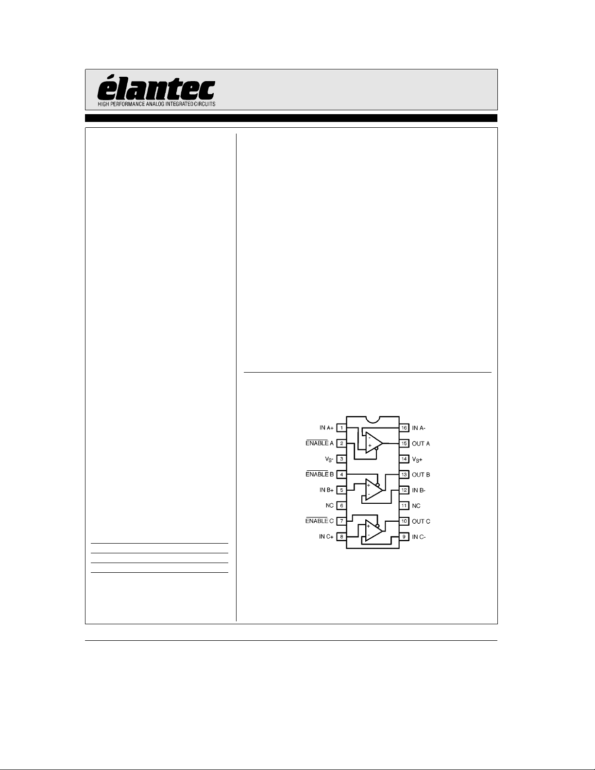
Connection Diagram
EL2386C SO, P-DIP
Ordering Information
Part No. Temp. Range Package Outline
EL2386CNb40§Ctoa85§C 16-Pin PDIP MDP0031
EL2386CSb40§Ctoa85§C 16-Pin SOIC MDP0027
Note: All information contained in this data sheet has been carefully checked and is believed to be accurate as of the date of publication; however, this data sheet cannot be a ‘‘controlled document’’. Current revisions, if any, to these
specifications are maintained at the factory and are available upon your request. We recommend checking the revision level before finalization of your design documentation.
©
1996 Elantec, Inc.
Ý
Manufactured under U.S. Patent No. 5,418,495.
Top View
2386-1
Page 2
EL2386C
250 MHz Triple Current Feedback Amp w/Disable
Absolute Maximum Ratings
Voltage between V
Common-Mode Input Voltage V
Differential Input Voltage
Current into
S
a
IN orbIN
a
and V
b
S
(T
S
A
b
g
e
a
12.6V
to V
g
7.5 mA
25§C)
Operating Ambient Temperature Range
Operating Junction Temperature 150
a
S
6V
Output Current
Storage Temperature Range
b
40§Ctoa85§C
g
b
65§Ctoa150§C
§
60 mA
Internal Power Dissipation See Curves
Important Note:
All parameters having Min/Max specifications are guaranteed. The Test Level column indicates the specific device testing actually
performed during production and Quality inspection. Elantec performs most electrical tests using modern high-speed automatic test
equipment, specifically the LTX77 Series system. Unless otherwise noted, all tests are pulsed tests, therefore T
Test Level Test Procedure
I 100% production tested and QA sample tested per QA test plan QCX0002.
II 100% production tested at T
III QA sample tested per QA test plan QCX0002.
IV Parameter is guaranteed (but not tested) by Design and Characterization Data.
V Parameter is typical value at T
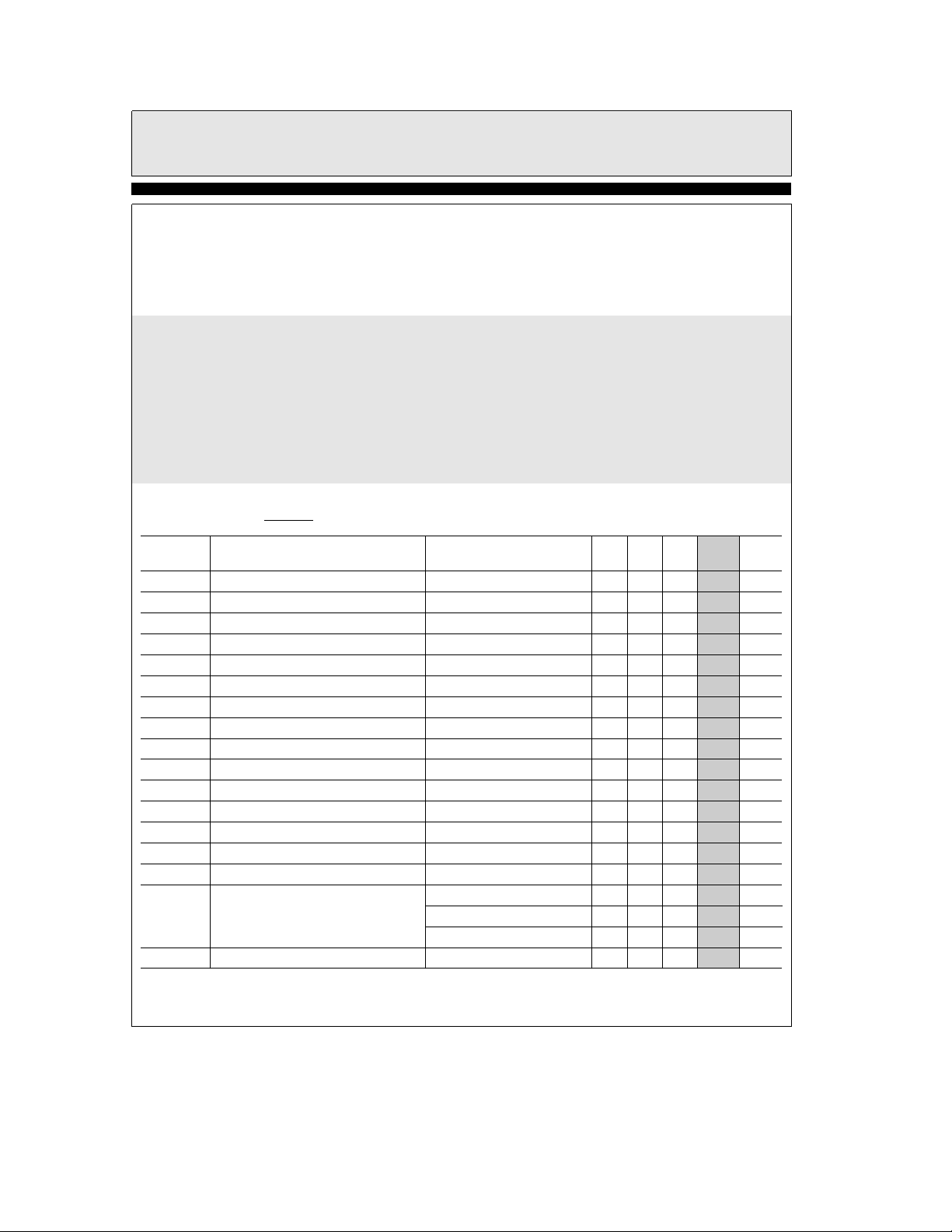
DC Electrical Characteristics
e
g
V
5V, R
S
T
and T
MAX
e
150X, ENABLEe0V, T
L
per QA test plan QCX0002.
MIN
e
25§C and QA sample tested at T
A
e
25§C for information purposes only.
A
e
25§C unless otherwise specified
A
e
25§C,
A
Parameter Description Conditions Min Typ Max
V
OS
TCV
OS
dV
OS
a
I
IN
daI
IN
b
I
IN
dbI
IN
CMRR Common Mode Rejection Ratio V
b
ICMR
PSRR Power Supply Rejection Ratio V
b
IPSR
R
OL
a
R
IN
a
C
IN
CMIR Common Mode Input Range
V
O
I
O
Input Offset Voltage 2.5 15 I mV
Average Input Offset Voltage Drift Measured from T
MIN
to T
MAX
VOS Matching 0.5 V mV
a
Input Current 1.5 15 I mA
a
IINMatching 20 V nA
b
Input Current 16 40 I mA
b
IINMatching 2VmA
e
g
3.5V 45 50 I dB
CM
b
Input Current Common Mode Rejection V
b
Input Current Power Supply Rejection V
Transimpedance V
a
Input Resistance V
a
Input Capacitance 1.2 V pF
Output Voltage Swing V
e
g
3.5V 5 30 I mA/V
CM
e
g
4V tog6V 60 70 I dB
S
e
g
4V tog6V 1 15 I mA/V
S
e
g
2.5V 120 300 I kX
e
g
3.5V 0.5 2 I MX
g
3.5g4.0 I V
e
g
5V
ea
5V Single-Supply, High 4.0 V V
ea
5V Single-Supply, Low 0.3 V V
g
3.5g4.0 I V
V
V
OUT
CM
S
S
S
Output Current 50 55 I mA
e
e
T
TA.
J
C
Test Units
Level
5VmV/§C
C
TDis 3.9in
2
Page 3
EL2386C
250 MHz Triple Current Feedback Amp w/Disable
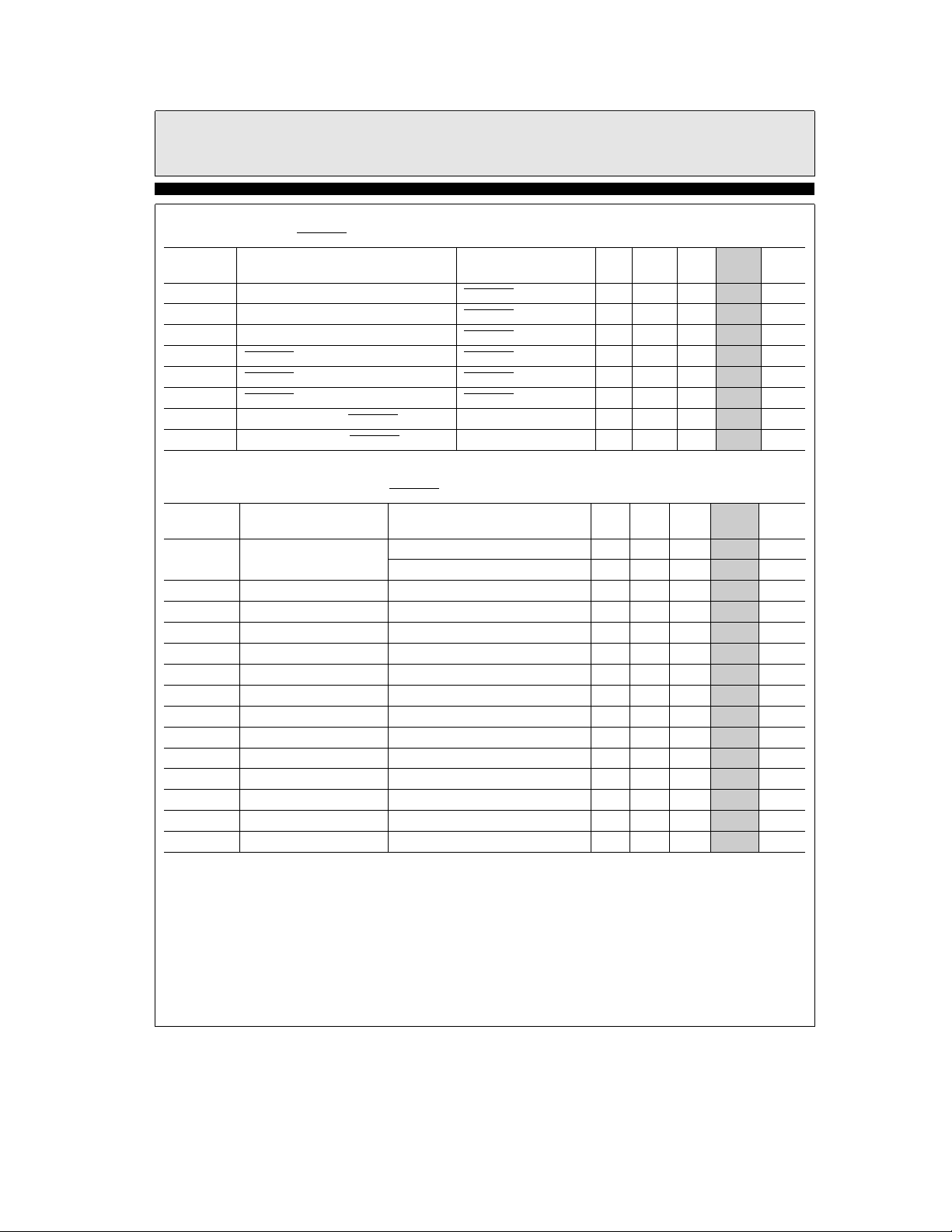
DC Electrical Characteristics
e
V
S
Parameter Description Conditions Min Typ Max
I
S
I
S(DIS)
C
OUT(DIS)
R
IN-EN
I
IH-EN
I
IL-EN
V
DIS
V
EN
AC Electrical Characteristics
e
g
V
S
Parameter Description Conditions Min Typ Max
BW
BW
SR Slew Rate V
tR,t
F
t
PD
OS Overshoot V
t
S
dG Differential Gain (Note 1) A
dP Differential Phase (Note 1) A
dG Differential Gain (Note 1) A
dP Differential Phase (Note 1) A
t
ON
t
OFF
CS Channel Separation fe5 MHz 85 V dB
Note 1: DC offset from 0V to 0.714V, AC amplitude 286 mV
Note 2: Measured from the application of the logic signal until the output voltage is at the 50% point between initial and final
g
5V, R
e
150 X, ENABLEe0V, T
L
e
25§C unless otherwise specified Ð Contd.
A
Supply CurrentÐEnabled (per amplifier) ENABLEe2.0V 3 6 I mA
e
Supply CurrentÐDisabled (per amplifier) ENABLE
4.5V 0 50 I mA
Output CapacitanceÐDisabled ENABLEe4.5V 4.4 V pF
ENABLE Pin Input Resistance ENABLEe2.0V to 4.5V 45 85 I kX
ENABLE Pin Input CurrentÐHigh ENABLEe4.5V
ENABLE Pin Input CurrentÐLow ENABLEe0V
b
0.04 V mA
b
53 V mA
Minimum Voltage at ENABLE to Disable 4.5 I V
Maximum Voltage at ENABLE to Enable 2.0 I V
e
5V, R
e
R
F
750 X,R
G
b
3 dB Bandwidth A
g
0.1 dB Bandwidth A
Rise and Fall Time V
Propagation Delay V
0.1% Settling V
Turn-On Time (Note 2) A
Turn-Off Time (Note 2) A
e
150X, ENABLEe0V, T
L
ea
V
ea
A
V
ea
V
OUT
e
OUT
e
OUT
e
OUT
e
OUT
ea
V
ea
V
ea
V
ea
V
ea
V
ea
V
e
25§C unless otherwise specified.
A
1 250 V MHz
2 180 V MHz
2 50 V MHz
e
g
2.5V, Measured atg1.25V 600 1200 IV V/ms
g
500 mV 1.5 V ns
g
500 mV 1.5 V ns
g
500 mV 3.0 V %
g
2, R
2, R
1, R
1, R
2, V
2, V
eb
2.5V, A
e
L
e
L
e
L
e
L
ea
IN
IN
,fe3.58 MHz.
p-p
115Vns
V
150X 0.05 V %
150X, 0.05 V
500X 0.01 V %
500X 0.01 V
e
ea
1V, R
1V, R
150X 40 100 I ns
L
e
150X 800 2000 I ns
L
values.
Test
Level
Test
Level
Units
Units
§
§
TDis 1.8inTDis 3.1in
3
Page 4
EL2386C
250 MHz Triple Current Feedback Amp w/Disable
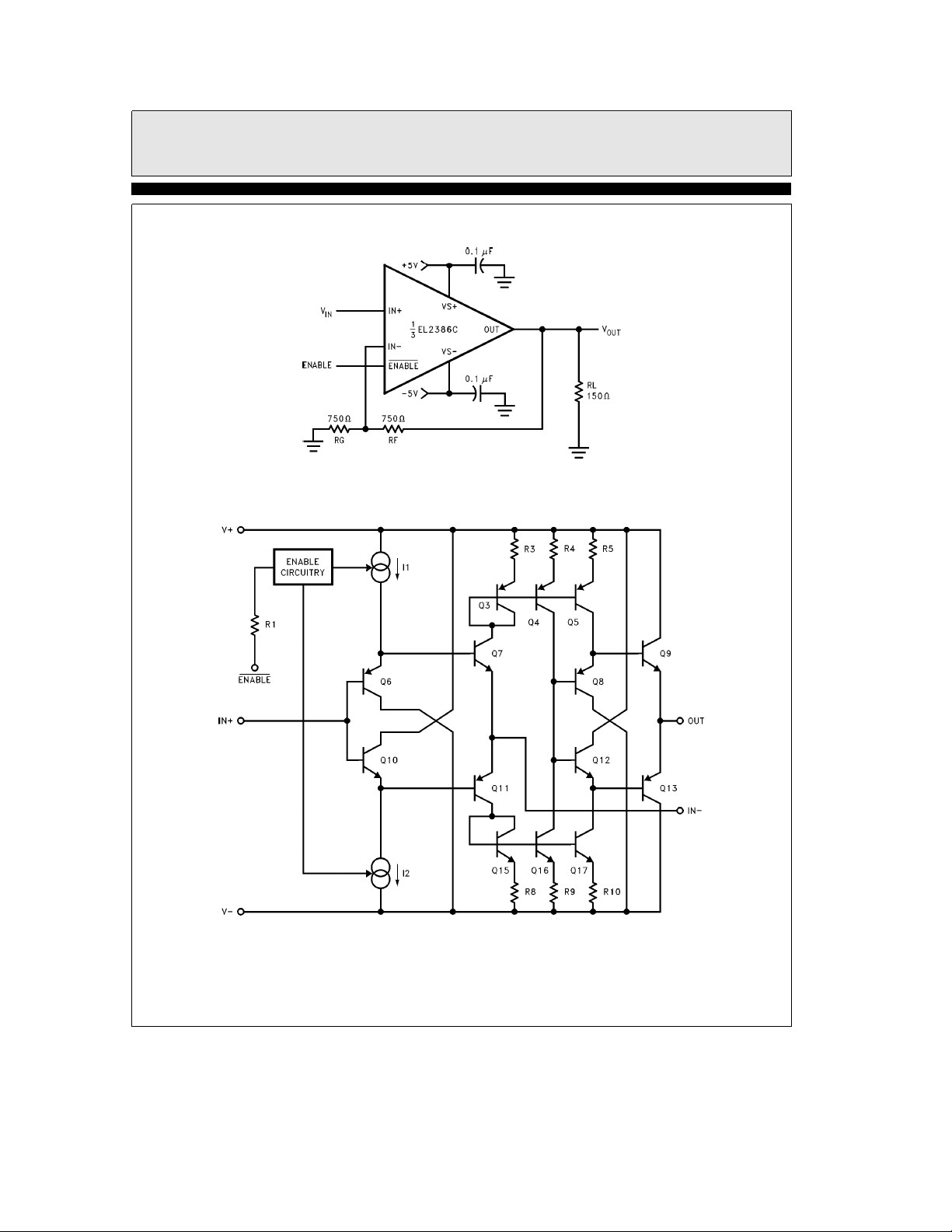
Test Circuit (per Amplifier)
Simplified Schematic (per Amplifier)
2386-2
2386-3
4
Page 5
EL2386C
250 MHz Triple Current Feedback Amp w/Disable
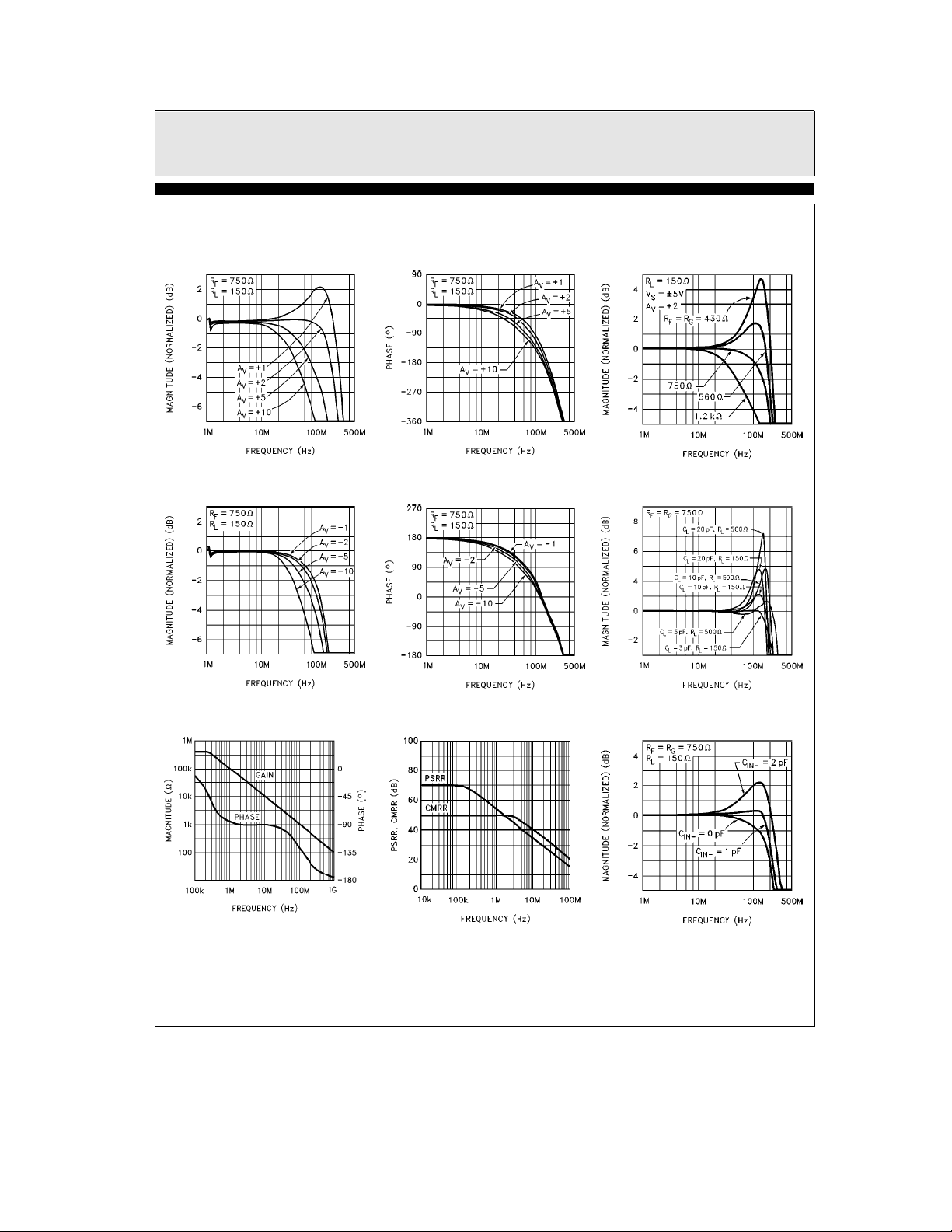
Typical Performance Curves
Non-Inverting Frequency
Response (Gain)
2386-4
Inverting Frequency
Response (Gain)
Ð Contd.
Non-Inverting Frequency
Response (Phase)
Inverting Frequency
Response (Phase)
2386-5
Frequency Response
for Various RFand R
Frequency Response
for Various RLand C
G
2386-6
L
Transimpedance (R
vs Frequency
OL
2386-7
)
2386-10
PSRR and CMRR
vs Frequency
2386-8
2386-11
Frequency Response for
Various C
b
IN
2386-9
2386-12
5
Page 6
EL2386C
250 MHz Triple Current Feedback Amp w/Disable
Typical Performance Curves
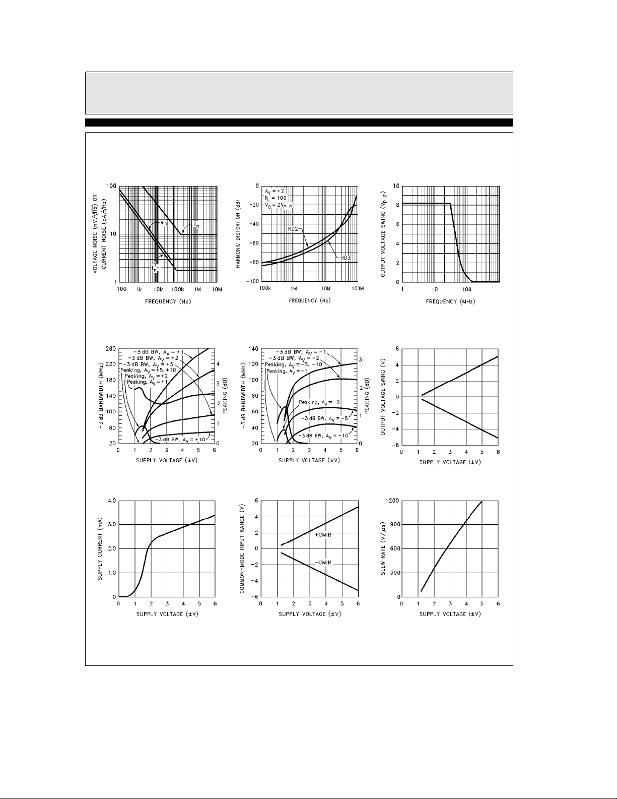
Voltage and Current
Noise vs Frequency
2386– 13
b
3 dB Bandwidth and Peaking
vs Supply Voltage for
Various Non-Inverting Gains
Ð Contd.
2nd and 3rd Harmonic
Distortion vs Frequency
b
3 dB Bandwidth and Peaking
vs Supply Voltage for
Various Inverting Gains
2386– 14
Output Voltage
Swing vs Frequency
Output Voltage Swing
vs Supply Voltage
2386– 15
Supply Current vs
Supply Voltage
2386– 16
2386– 19
Common-Mode Input Range
vs Supply Voltage
2386– 20
6
2386– 17
Slew Rate vs
Supply Voltage
2386– 18
2386– 21
Page 7
EL2386C
250 MHz Triple Current Feedback Amp w/Disable
Typical Performance Curves
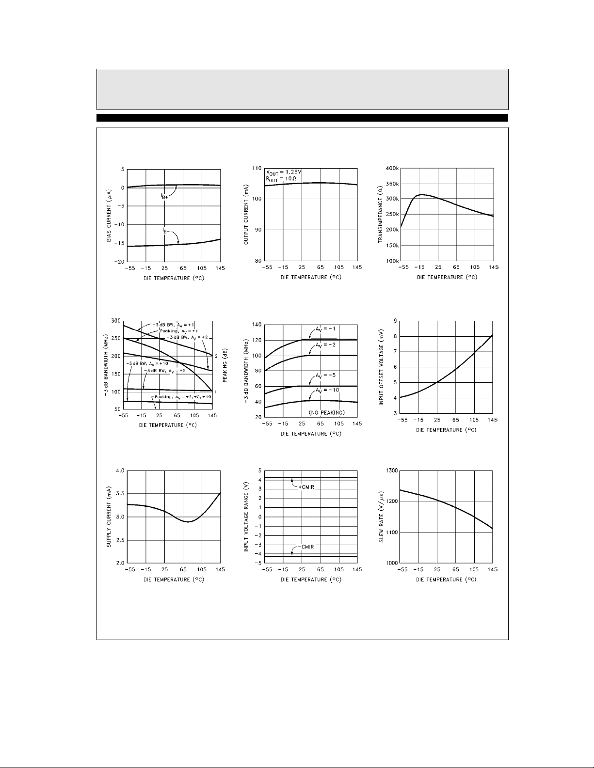
Input Bias Current
vs Die Temperature
2386-22
b
3 dB Bandwidth and Peaking
vs Die Temperature for
Various Non-Inverting Gains
Ð Contd.
Short-Circuit Current
vs Die Temperature
b
3 dB Bandwidth vs
Die Temperature for
Various Inverting Gains
2386-23
Transimpedance (R
vs Die Temperature
Input Offset Voltage
vs Die Temperature
OL
)
2386-24
Supply Current vs
Die Temperature
2386-25
2386-28
Input Voltage Range
vs Die Temperature
7
2386-26
2386-29
Slew Rate vs
Die Temperature
2386-27
2386-30
Page 8
EL2386C
250 MHz Triple Current Feedback Amp w/Disable
Typical Performance Curves
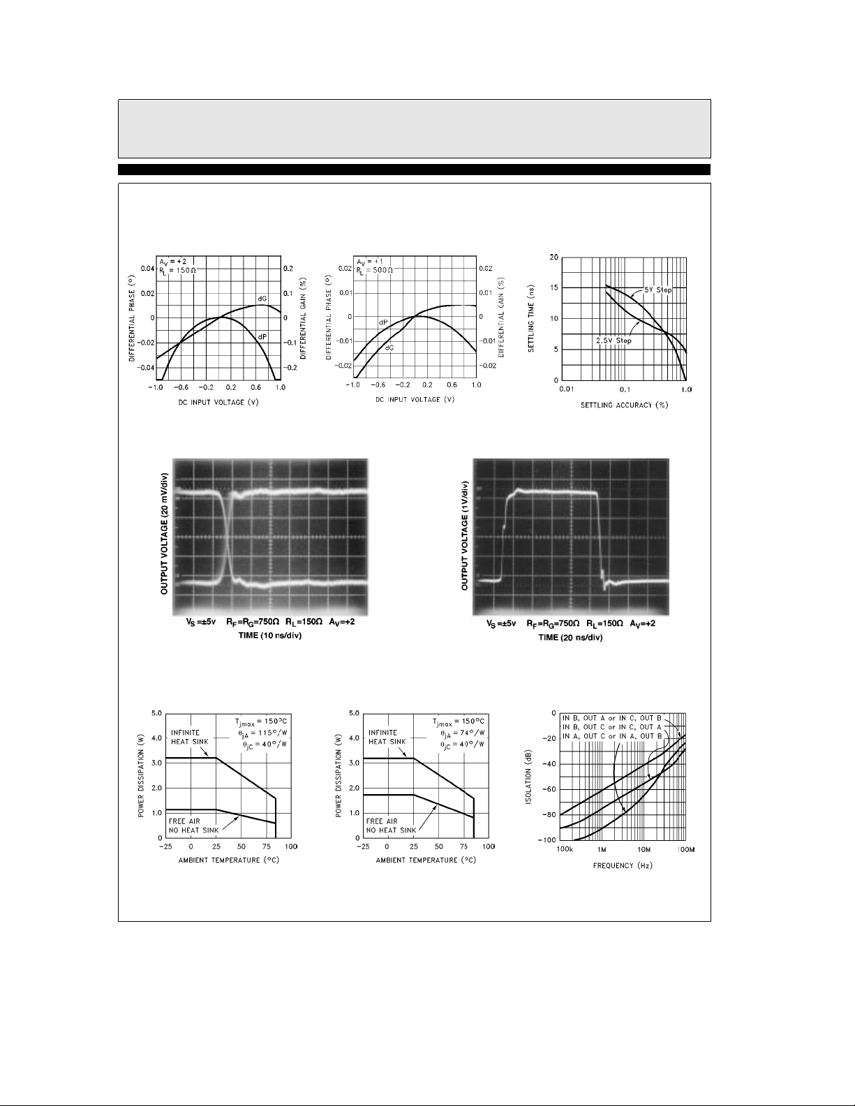
Differential Gain and
Phase vs DC Input
Voltage at 3.58 MHz
2386-31
Small-Signal Step Response
Ð Contd.
Differential Gain and
Phase vs DC Input
Voltage at 3.58 MHz
Settling Time vs
Settling Accuracy
2386-32
Large-Signal Step Response
2386-33
16-Pin Plastic DIP
Maximum Power Dissipation
vs Ambient Temperature
2386-36
2386-34
16-Lead SO
Maximum Power Dissipation
vs Ambient Temperature
2386-37
8
Channel to Channel
Isolation vs Frequency
2386-35
2386-38
Page 9
250 MHz Triple Current Feedback Amp w/Disable
Applications Information
Product Description
The EL2386C is a current-feedback operational
amplifier that offers a wide
250 MHz, a low supply current of 3 mA per amplifier and the ability to power down to 0 mA. It
also features high output current drive. The
EL2386C can output 55 mA per amplifier. The
EL2386C works with supply voltages ranging
from a single 3V to
swinging to within 1V of either supply on the
input and the output. Because of its current-feedback topology, the EL2386C does not have the
normal gain-bandwidth product associated with
voltage-feedback operational amplifiers. This allows its
constant as closed-loop gain is increased. This
combination of high bandwidth and low power,
together with aggressive pricing make the
EL2386C the ideal choice for many low-power/
high-bandwidth applications such as portable
computing, HDSL, and video processing.
For Single and Dual applications, consider the
EL2186C/EL2286C. For Single, Dual and Quad
applications without disable, consider the
EL2180C, EL2280C, or EL2480C, all in industry
standard pin outs. The EL2180C also is available
in the tiny SOT-23 package, which is 28% the
size of an SO8 package. For lower power applications where speed is still a concern, consider the
EL2170C/EL2176C family which also comes in
similar Single, Dual and Quad configurations
with 70 MHz of bandwidth while consuming
1 mA of supply current per amplifier.
b
3 dB bandwidth to remain relatively
g
Power Supply Bypassing and Printed
Circuit Board Layout
As with any high-frequency device, good printed
circuit board layout is necessary for optimum
performance. Ground plane construction is highly recommended. Lead lengths should be as short
as possible. The power supply pins must be well
bypassed to reduce the risk of oscillation. The
combination of a 4.7 mF tantalum capacitor in
parallel with a 0.1 mF capacitor has been shown
to work well when placed at each supply pin. For
single supply operation, where pin 3 (V
b
3 dB bandwidth of
6V, and it is also capable of
) is con-
S-
EL2386C
nected to the ground plane, a single 4.7 mF tantalum capacitor in parallel with a 0.1 mF ceramic
capacitor across pins 14 and 3 will suffice.
For good AC performance, parasitic capacitance
should be kept to a minimum especially at the
inverting input (see the Capacitance at the Inverting Input section). Ground plane construction should be used, but it should be removed
from the area near the inverting input to minimize any stray capacitance at that node. Carbon
or Metal-Film resistors are acceptable with the
Metal-Film resistors giving slightly less peaking
and bandwidth because of their additional series
inductance. Use of sockets, particularly for the
SO package should be avoided if possible. Sockets add parasitic inductance and capacitance
which will result in some additional peaking and
overshoot.
Disable/Power-Down
The EL2386C amplifier can be disabled, placing
its output in a high-impedance state. When disabled, the supply current is reduced to 0 mA. The
EL2386C is disabled when its ENABLE
floating or pulled up to within 0.5V of the positive supply. Similarly, the amplifier is enabled by
pulling its ENABLE
positive supply. For
that an EL2386C amplifier will be enabled when
ENABLE
ENABLE
els are not standard TTL, this choice of logic
voltages allows the EL2386C to be enabled by tying ENABLE
supply applications. The ENABLE
driven from CMOS outputs or open-collector
TTL.
When enabled, supply current does vary somewhat with the voltage applied at ENABLE
example, with the supply voltages of the
EL2186C at
(rather than ground) the supply current will increase about 15% to 3.45 mA.
is at 2V or less, and disabled when
is above 4.5V. Although the logic lev-
g
pin at least 3V below the
g
5V supplies, this means
to ground, even ina3V single-
5V, if ENABLE is tied tob5V
pin is
pin can be
. For
9
Page 10

EL2386C
250 MHz Triple Current Feedback Amp w/Disable
Applications Information
Ð Contd.
Capacitance at the Inverting Input
Any manufacturer’s high-speed voltage- or current-feedback amplifier can be affected by stray
capacitance at the inverting input. For inverting
gains this parasitic capacitance has little effect
because the inverting input is a virtual ground,
but for non-inverting gains this capacitance (in
conjunction with the feedback and gain resistors)
creates a pole in the feedback path of the amplifier. This pole, if low enough in frequency, has the
same destabilizing effect as a zero in the forward
open-loop response. The use of large value feedback and gain resistors further exacerbates the
problem by further lowering the pole frequency.
The experienced user with a large amount of PC
board layout experience may find in rare cases
that the EL2386C has less bandwidth than expected. In this case, the inverting input may have
less parasitic capacitance than expected. The reduction of feedback resistor values (or the addition of a very small amount of external capacitance at the inverting input, e. g. 0.5 pF) will
increase bandwidth as desired. Please see the
curves for Frequency Response for Various R
and RG, and Frequency Response for Various
C
.
IN-
Feedback Resistor Values
The EL2386C has been designed and specified at
gains of
a
1 anda2 with R
of feedback resistor gives 250 MHz of
bandwidth at A
V
ea
peaking, and 180 MHz of
ea
A
V
2 with about 0.1 dB of peaking. Since
e
750X. This value
F
b
3dB
1 with about 2.5 dB of
b
3 dB bandwidth at
the EL2386C is a current-feedback amplifier, it is
also possible to change the value of R
F
to get
more bandwidth. As seen in the curve of Frequency Response For Various R
and RG, band-
F
width and peaking can be easily modified by
varying the value of the feedback resistor.
Because the EL2386C is a current-feedback amplifier, its gain-bandwidth product is not a constant for different closed-loop gains. This feature
actually allows the EL2386C to maintain about
the same
b
3 dB bandwidth, regardless of closed-
loop gain. However, as closed-loop gain is in-
creased, bandwidth decreases slightly while stability increases. Since the loop stability is improving with higher closed-loop gains, it becomes
possible to reduce the value of R
below the spec-
F
ified 750X and still retain stability, resulting in
only a slight loss of bandwidth with increased
closed-loop gain.
Supply Voltage Range and SingleSupply Operation
The EL2386C has been designed to operate with
supply voltages having a span of greater than 3V,
and less than 12V. In practical terms, this means
that the EL2386C will operate on dual supplies
ranging from
g
1.5V tog6V. With a single-sup-
ply, the EL2386C will operate from
a
12V.
As supply voltages continue to decrease, it becomes necessary to provide input and output
voltage ranges that can get as close as possible to
the supply voltages. The EL2386C has an input
voltage range that extends to within 1V of either
supply. So, for example, on a single
the EL2386C has an input range which spans
F
from 1V to 4V. The output range of the EL2386C
is also quite large, extending to within 1V of the
supply rail. On a
therefore capable of swinging from
g
5V supply, the output is
b
Single-supply output range is even larger because
of the increased negative swing due to the external pull-down resistor to ground. On a single
a
5V supply, output voltage range is about 0.3V
to 4V.
Video Performance
For good video performance, an amplifier is required to maintain the same output impedance
and the same frequency response as DC levels are
changed at the output. This is especially difficult
when driving a standard video load of 150X, because of the change in output current with DC
level. Until the EL2386C, good Differential Gain
could only be achieved by running high idle currents through the output transistors (to reduce
variations in output impedance). These currents
were typically comparable to the entire 3 mA
supply current of each EL2386C amplifier! Spe-
a
3V to
a
5V supply,
4V toa4V.
10
Page 11
EL2386C
250 MHz Triple Current Feedback Amp w/Disable
Applications Information
cial circuitry has been incorporated in the
EL2386C to reduce the variation of output impedance with current output. This results in dG
and dP specifications of 0.05% and 0.05
driving 150X at a gain of
Video Performance has also been measured with
a 500X load at a gain of
tions, the EL2386C has dG and dP specifications
of 0.01% and 0.01
500X at A
For complete curves, see the Differential Gain
and Differential Phase vs Input Voltage curves.
V
ea
1.
a
2.
a
1. Under these condi-
respectively while driving
§
Ð Contd.
while
§
Output Drive Capability
In spite of its low 3 mA of supply current per
amplifier, the EL2386C is capable of providing a
minimum of
output drive level is unprecedented in amplifiers
running at these supply currents. With a mini-
g
mum
capable of driving 50X loads to
an excellent choice for driving multiple video
loads in RGB applications.
g
50 mA of output current. This
50 mA of output drive, the EL2386C is
g
2.5V, making it
Driving Cables and Capacitive Loads
When used as a cable driver, double termination
is always recommended for reflection-free performance. For those applications, the back-termination series resistor will decouple the EL2386C
from the cable and allow extensive capacitive
drive. However, other applications may have
high capacitive loads without a back-termination
resistor. In these applications, a small series resistor (usually between 5X and 50X) can be placed
in series with the output to eliminate most peaking. The gain resistor (R
make up for any gain loss which may be created
by this additional resistor at the output. In many
cases it is also possible to simply increase the value of the feedback resistor (R
peaking.
) can then be chosen to
G
) to reduce the
F
Current Limiting
The EL2386C has no internal current-limiting
circuitry. If an output is shorted indefinitely, the
power dissipation could easily increase such that
the part will be destroyed. Maximum reliability
is maintained if the output current never exceeds
g
60 mA. A heat sink may be required to keep
the junction temperature below absolute maximum when an output is shorted indefinitely.
Multiplexing with the EL2386C
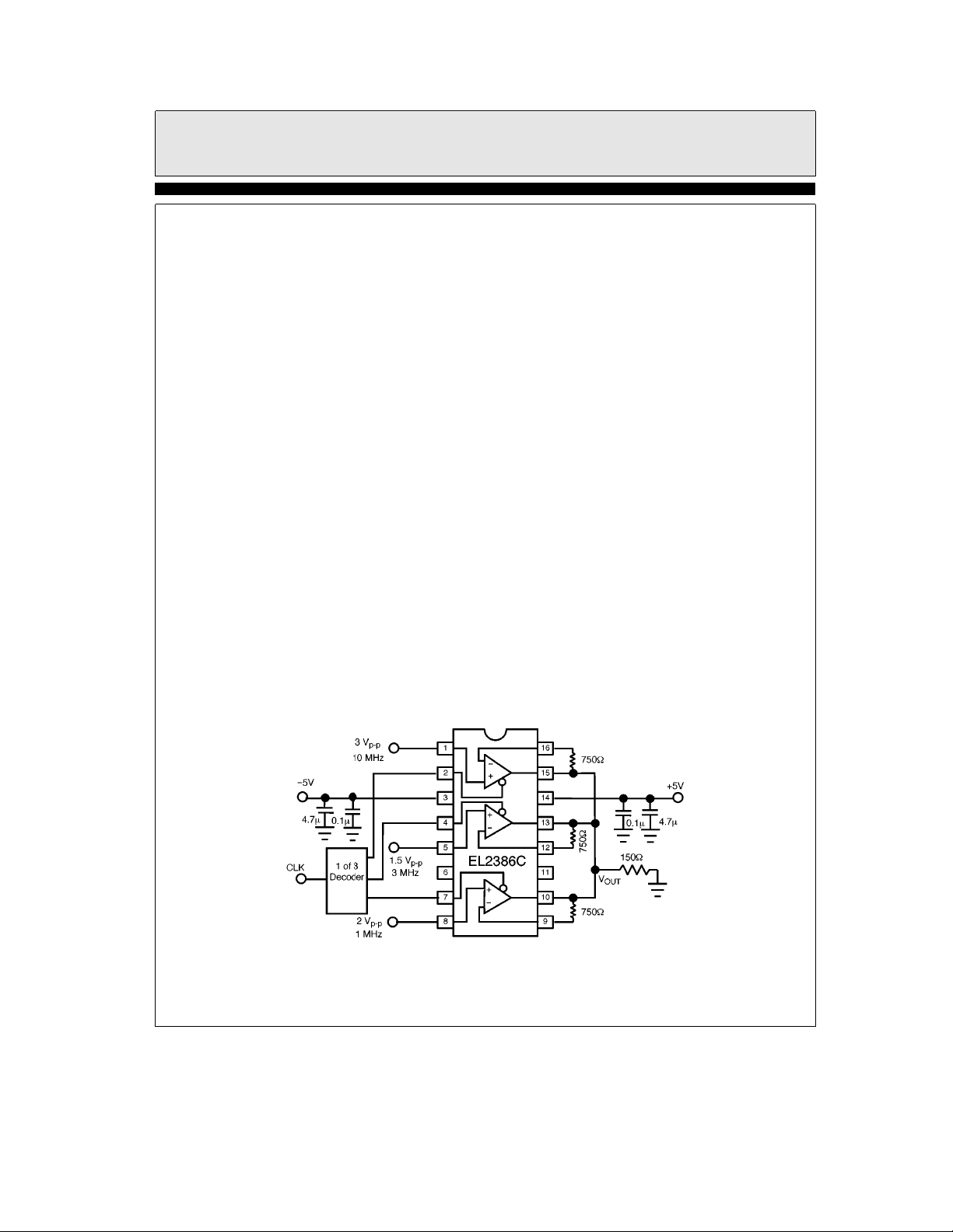
The ENABLE pins on the EL2386C allow for
multiplexing applications. Figure 1 shows an
EL2386C with all 3 outputs tied together, driving
a back terminated 75X video load. Three sine
waves of varying amplitudes and frequencies are
applied to the three inputs, whilea1of3decoder
selects one amplifier to be on at any given time.
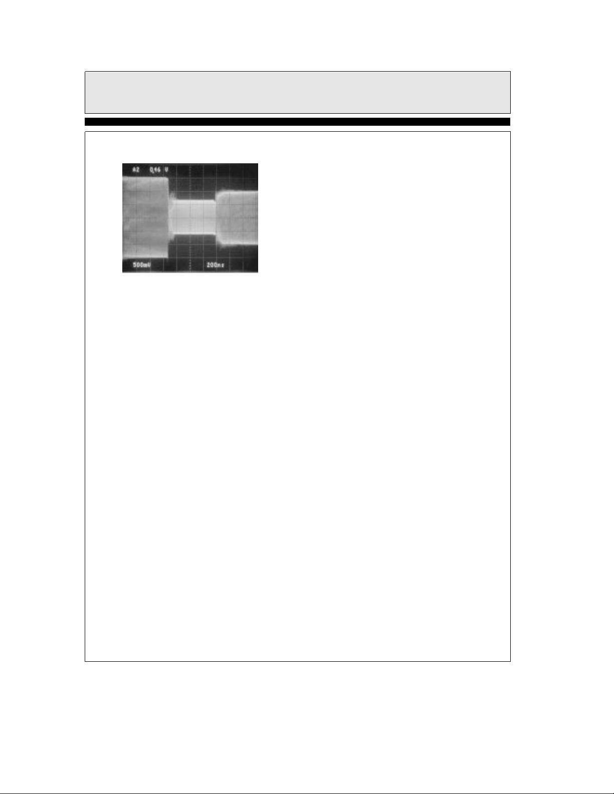
Figure 2 shows the resulting output wave form at
Figure 1
11
2386-39
Page 12
EL2386C
250 MHz Triple Current Feedback Amp w/Disable
Applications Information
Figure 2
V
. Switching is complete in about 100 ns.
OUT
Ð Contd.
2386-40
Notice the outputs are tied directly together. Decoupling resistors at each output are not required
or advised when multiplexing.
Power Dissipation
With the high output drive capability of the
EL2386C, it is possible to exceed the 150
C Abso-
§
lute Maximum junction temperature under certain very high load current conditions. Generally
speaking, when R
falls below about 25X,itis
L
important to calculate the maximum junction
temperature (T
) for the application to deter-
Jmax
mine if power-supply voltages, load conditions,
or package type need to be modified for the
EL2386C to remain in the safe operating area.
These parameters are calculated as follows:
T
JMAX
e
T
MAX
a
(iJA* n * PD
MAX
)
where:
e
T
i
JA
n
PD
MAX
e
Maximum Ambient Temperature
e
Thermal Resistance of the Package
Number of Amplifiers in the Package
e
MAX
Maximum Power Dissipation of
Each Amplifier in the Package.
PD
for each amplifier can be calculated as
MAX
follows:
PD
MAX
(VS–V
e
(2 * VS* I
OUTMAX
) * (V
OUTMAX/RL
SMAX
a
)
)
where:
e
V
Supply Voltage
S
SMAX
e
Maximum Supply Current of 1
I
Amplifier
V
OUTMAX
e
Max. Output Voltage of the
Application
e
R
Load Resistance
L
[1]
[2]
12
Page 13

EL2386C
250 MHz Triple Current Feedback Amp w/Disable
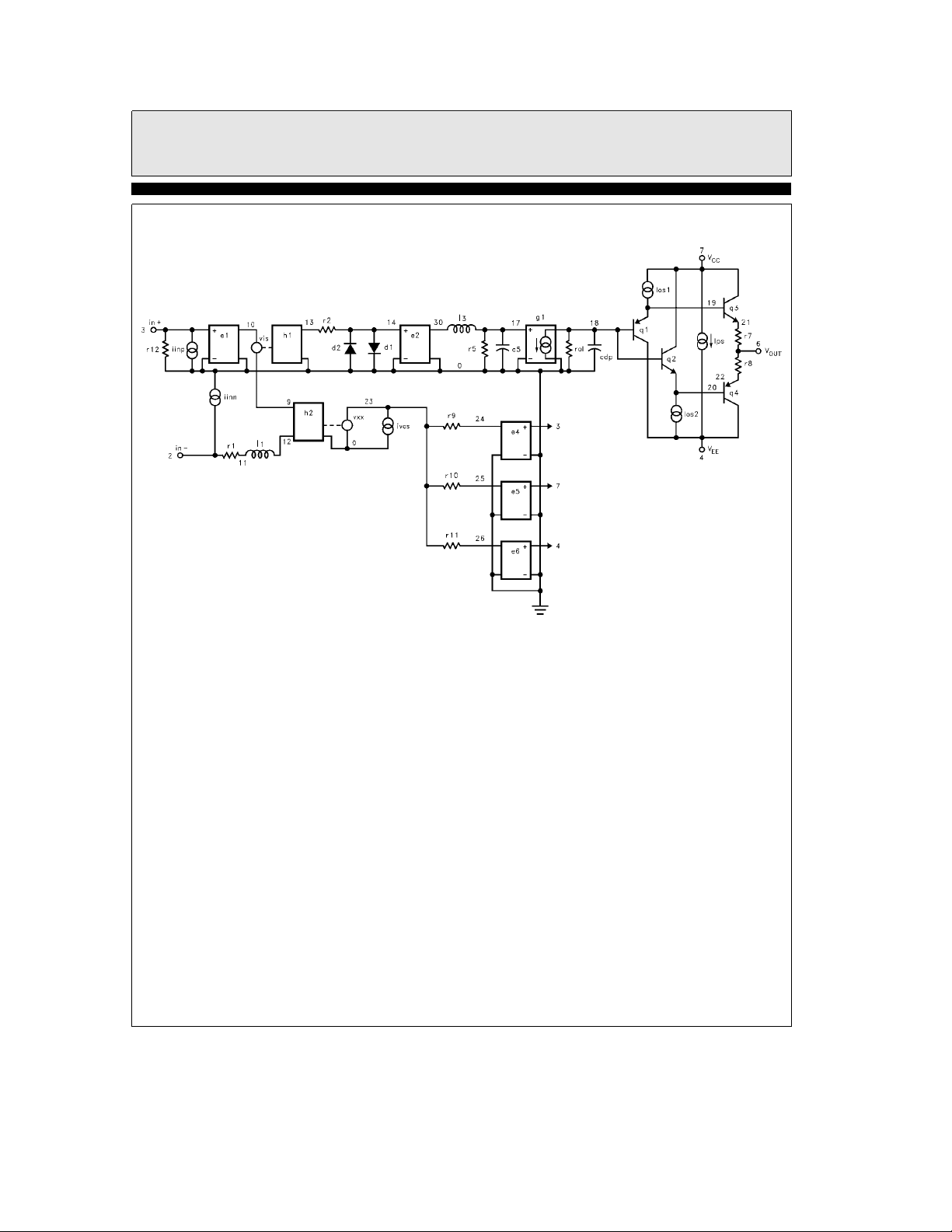
EL2386C Macromodel
* EL2386C Macromodel
* Revision A, July 1996
* AC characteristics used: Rf
* Pin numbers reflect a standard single opamp
* Connections:
*
*
*
*
*
.subckt EL2386/EL 3 2 7 4 6
*
* Input Stage
*
e1100301.0
vis 10 9 0V
h2 9 12 vxx 1.0
r1211400
l1 11 12 25nH
iinp 3 0 1.5mA
iinm203mA
r12 3 0 2Meg
*
* Slew Rate Limiting
*
h1 13 0 vis 600
r2 13 14 1K
d1 14 0 dclamp
d2 0 14 dclamp
*
* High Frequency Pole
*
e2 30 0 14 0 0.00166666666
l3 30 17 150nH
c5 17 0 0.8pF
r5 17 0 165
*
eRge
750 ohms
a
input
b
input
l
ll
lll
a
V
supply
b
V
supply
llll
lllll
output
* Transimpedance Stage
*
g10181701.0
rol 18 0 450k
cdp 18 0 0.675pF
*
* Output Stage
*
q141819qp
q271820qn
q371921qn
q442022qp
r7 21 6 4
r8 22 6 4
ios1 7 19 1mA
ios2 20 4 1mA
*
* Supply Current
*
ips 7 4 0.2mA
*
* Error Terms
*
ivos 0 23 0.2mA
vxx 23 0 0V
e4240301.0
e5250701.0
e626040
r9 24 23 316
r10 25 23 3.2K
r11 26 23 3.2K
*
* Models
*
.model qn npn(is
.model qp pnp(is
.model dclamp d(is
abve
.ends
b
1.0
0.71v ne4)
e5eb
e5eb
e1eb
15 bfe200 tfe0.1nS)
15 bfe200 tfe0.1nS)
30 ibve0.266
TABWIDE
TDis 4.8in
TDis 5.1in
13
Page 14
EL2386C
250 MHz Triple Current Feedback Amp w/Disable
EL2386C Macromodel
Ð Contd.
2386-41
14
Page 15

BLANK
15
Page 16
EL2386C
250 MHz Triple Current Feedback Amp w/Disable
EL2386CJune 1996 Rev A
General Disclaimer
Specifications contained in this data sheet are in effect as of the publication date shown. Elantec, Inc. reserves the right to make changes
in the circuitry or specifications contained herein at any time without notice. Elantec, Inc. assumes no responsibility for the use of any
circuits described herein and makes no representations that they are free from patent infringement.
WARNING Ð Life Support Policy
Elantec, Inc. products are not authorized for and should not be
used within Life Support Systems without the specific written
consent of Elantec, Inc. Life Support systems are equipment in-
Elantec, Inc.
1996 Tarob Court
Milpitas, CA 95035
Telephone: (408) 945-1323
(800) 333-6314
Fax: (408) 945-9305
European Office: 44-71-482-4596
tended to support or sustain life and whose failure to perform
when properly used in accordance with instructions provided can
be reasonably expected to result in significant personal injury or
death. Users contemplating application of Elantec, Inc. products
in Life Support Systems are requested to contact Elantec, Inc.
factory headquarters to establish suitable terms & conditions for
these applications. Elantec, Inc.’s warranty is limited to replacement of defective components and does not cover injury to persons or property or other consequential damages.
Printed in U.S.A.16
 Loading...