

Datasheet EL2280CS-T7, EL2280CS-T13, EL2280CS, EL2480CS-T7, EL2480CS-T13 Datasheet (ELANT)
...Page 1
EL2180C/EL2280C/EL2480C-Preliminary
250MHz / 3mA Current Mode Feedback Amplifiers
EL2180C/EL2280C/EL2480C-
Features
• Single, dual, and quad topologies
• 3mA supply current (per amplifier)
• 250MHz -3dB bandwidth
• 1200V/µs slew rate
• Tiny package package options
(SOT23, LPP)
• Low cost
• Single- and dual-supply operation
down to ±1.5V
• 0.05%/0.05° diff. gain/diff. phase
into 150Ω
Applications
• Low power/battery applications
• HDSL amplifiers
• Video amplifiers
• Cable drivers
• RGB amplifiers
• Test equipment amplifiers
• Current to voltage converters
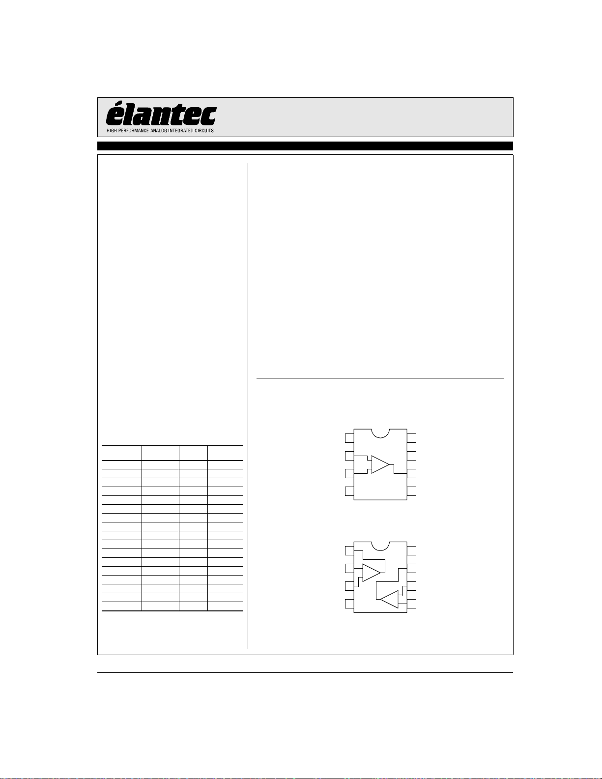
Ordering Information
Part No Package
EL2180CN 8-Pin PDIP - MDP0031
EL2180CS 8-Pin SO - MDP0027
EL2180CS-T7 8-Pin SO 7” MDP0027
EL2180CS-T13 8-Pin SO 13” MDP0027
EL2180CW-T7 5-Pin SOT23 7” MDP0038
EL2180CW-T13 5-Pin SOT23 13” MDP0038
EL2280CN 8-Pin PDIP - MDP0031
EL2280CS 8-Pin SO - MDP0027
EL2280CS-T7 8-Pin SO 7” MDP0027
EL2280CS-T13 8-Pin SO 13” MDP0027
EL2480CN 14-Pin PDIP - MDP0031
EL2480CS 14-Pin SO - MDP0027
EL2480CS-T7 14-Pin SO 7” MDP0027
EL2480CS-T13 14-Pin SO 13” MDP0027
EL2480CL 24-Pin LPP - MDP0046
EL2480CL-T7 24-Pin LPP 7” MDP0046
EL2480CL-T13 24-Pin LPP 13” MDP0046
Tape &
Reel Outline #
General Description
The EL2180C/EL2280C/EL2480C are single/dual/quad current-feedback operational amplifiers that achieve a -3dB bandwidth of 250MHz
at a gain of +1 while consuming only 3mA of supply current per
amplifier. They will operate with dual supplies ranging from ±1.5V to
±6V or from single supplies ranging from +3V to +12V. In spite of
their low supply current, the EL2480C and the EL2280C can output
55mA while swinging to ±4V on ±5V supplies. The EL2180C can output 100mA with similar output swings. These attributes make the
EL2180C/EL2280C/EL2480C excellent choices for low power and/or
low voltage cable driver, HDSL, or RGB applications.
For applications where board space is extremely critical, the EL2180C
is available in the tiny 5-pin SOT23 package, with a footprint size 28%
of an 8-pin SO. The EL2480C is also available in a 24-pin LPP package. All are specified for operation over the full -40°C to +85°C
temperature range.
Single, dual, and triple versions are also available with the enable
function (EL2186C, EL2286C, and EL2386C).
Connection Diagrams
OUTA
INA-
INA+
IN+
VS-
VS-
1
NC
2
IN-
3
4
1
2
3
4
-
+
EL2180C
(8-Pin SO & 8-Pin PDIP)
A
+
EL2280C
(8-Pin SO & 8-Pin PDIP)
8
NC
7
VS+
6
OUT
5
NC
8
VS+
7
OUTB
6
INB-
-
B
5
INB+
+
July 19, 2001
Note: All information contained in this data sheet has been carefully checked and is believed to be accurate as of the date of publication; however, this data sheet cannot be a “controlled document”. Current revisions, if any, to these
specifications are maintained at the factory and are available upon your request. We recommend checking the revision level before finalization of your design documentation.
© 2001 Elantec Semiconductor, Inc.
Page 2

EL2180C/EL2280C/EL2480C-Preliminary
250MHz / 3mA Current Mode Feedback Amplifiers
Absolute Maximum Ratings (T
Supply Voltage between VS+ and GND +12.6V
Voltage between VS+ and VS- +12.6V
Common-Mode Input Voltage VS- to VS+
Differential Input Voltage ±6V
Current into +IN or -IN ±7.5mA
Internal Power Dissipation See Curves
Operating Ambient Temperature Range -40°C to +85°C
Important Note:
All parameters having Min/Max specifications are guaranteed. Typ values are for information purposes only. Unless otherwise noted, all tests are at the
specified temperature and are pulsed tests, therefore: TJ = TC = TA.
= 25°C)
A
Operating Junction Temperature
Plastic Packages 150°C
Output Current (EL2180C) ±120mA
Output Current (EL2280C) ±60mA
Output Current (EL2480C) ±60mA
Storage Temperature Range -65°C to +150°C
DC Electrical Characteristics
VS = ±5V, R
EL2180C/EL2280C/EL2480C-Preliminary
Parameter Description Conditions Min Typ Max Unit
V
TCV
dV
+I
d+I
-I
IN
d-I
CMRR Common Mode Rejection Ratio VCM = ±3.5V 45 50 dB
-ICMR -Input Current Common Mode Rejection VCM = ±3.5V 5 30 µA/V
PSRR Power Supply Rejection Ratio VS is moved from ±4V to ±6V 60 70 dB
-IPSR -Input Current Power Supply Rejection VS is moved from ±4V to ±6V 1 15 µA/V
R
OL
+R
+C
CMIR Common Mode Input Range ±3.5 ±4.0 V
V
I
O
I
S
= 150Ω, T
L
OS
OS
OS
IN
IN
IN
IN
IN
O
= 25°C unless otherwise specified.
A
Input Offset Voltage 2.5 10 mV
Average Input Offset Voltage Drift Measured from T
VOS Matching EL2280C, EL2480C only 0.5 mV
+Input Current 1.5 15 µA
+IIN Matching EL2280C, EL2480C only 20 nA
-Input Current 16 40 µA
-IIN Matching EL2280C, EL2480C only 2 µA
Transimpedance V
+Input Resistance V
+Input Capacitance 1.2 pF
Output Voltage Swing VS = ±5 ±3.5 ±4.0 V
Output Current EL2180C only 80 100 mA
Supply Current Per amplifier 3 6 mA
= ±2.5V 120 300 kΩ
OUT
= ±3.5V 0.5 2 MΩ
CM
VS = +5 Single-supply, high 4.0 V
VS = +5 Single-supply, low 0.3 V
EL2280C only, per amplifier 50 55 mA
EL2480C only, per amplifier 50 55 mA
MIN
to T
MAX
5 µV/°C
AC Electrical Characteristics
VS = ±5V, RF = R
Parameter Description Conditions Min Typ Max Unit
-3dB BW -3dB Bandwidth AV = +1 250 MHz
-3dB BW -3dB Bandwidth AV = +2 180 MHz
0.1dB BW 0.1dB Bandwidth AV = +2 50 MHz
SR Slew Rate V
tR, t
F
= 750Ω for PDIP and SO packages, R
G
Rise and Fall Time V
F
= R
= 560Ω for SOT23-5 package, RL = 150Ω, T
G
= ±2.5V, AV = +2 600 1200 V/µs
OUT
= ±500 mV 1.5 ns
OUT
= 25°C unless otherwise specified
A
2
Page 3
EL2180C/EL2280C/EL2480C-Preliminary
250MHz / 3mA Current Mode Feedback Amplifiers
AC Electrical Characteristics
VS = ±5V, RF = R
Parameter Description Conditions Min Typ Max Unit
t
PD
OS Overshoot V
t
S
dG Differential Gain AV = +2, R
dP Differential Phase AV = +2, R
dG Differential Gain AV = +1, R
dP Differential Phase AV = +1, R
C
S
1. DC offset from 0V to 0.714V, AC amplitude 286mV
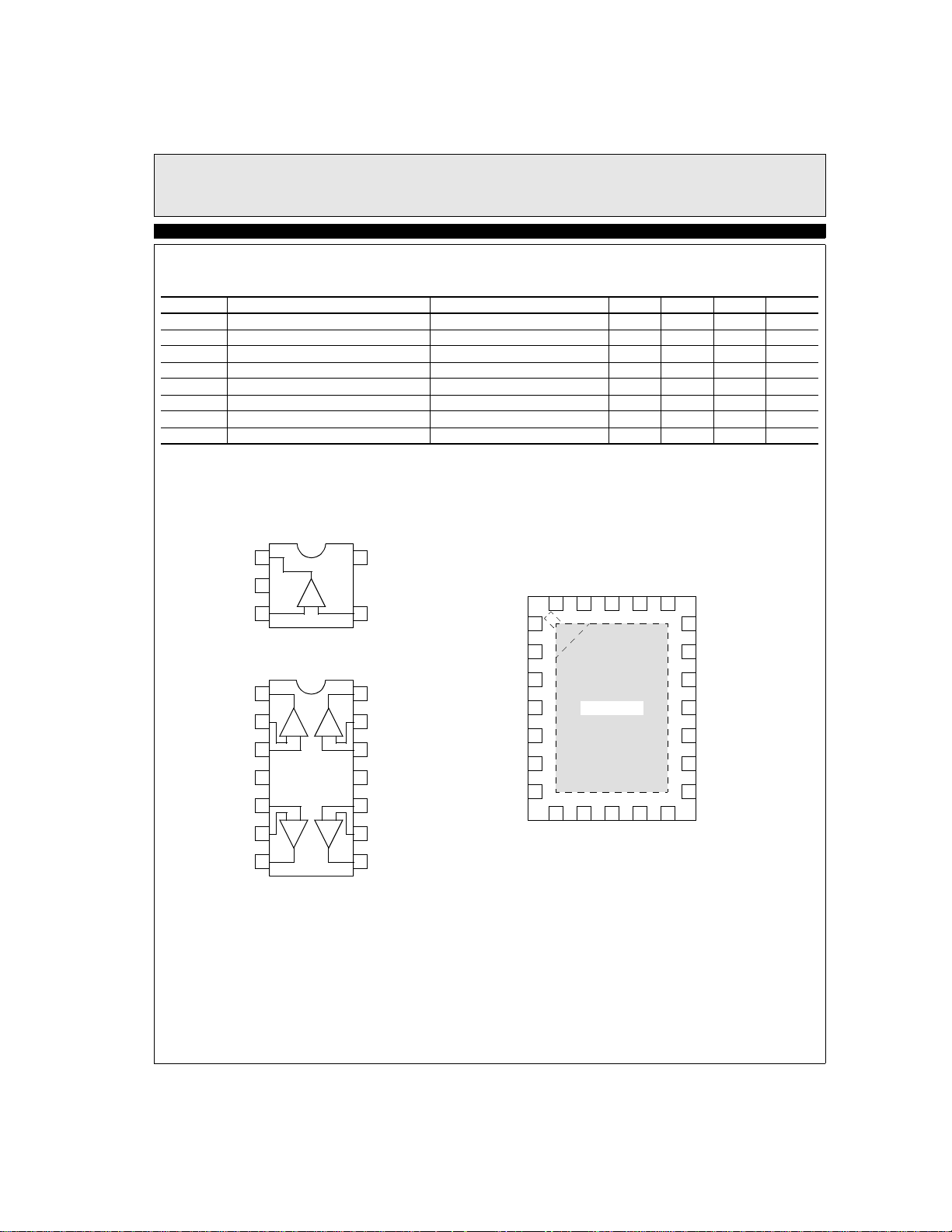
Connection Diagrams (Continued)
= 750Ω for PDIP and SO packages, R
G
Propagation Delay V
0.1% Settling V
= R
= 560Ω for SOT23-5 package, RL = 150Ω, T
F
G
= ±500 mV 1.5 ns
OUT
= ±500 mV 3.0 %
OUT
= ±2.5V, AV = -1 15 ns
OUT
= 150Ω
L
= 150Ω
L
= 500Ω
L
= 500Ω
L
[1]
[1]
[1]
[1]
= 25°C unless otherwise specified
A
0.05 %
0.05 °
0.01 %
0.01 °
Channel Separation EL2280C, EL2480C only, f = 5 MHz 85 dB
, f = 3.58MHz
P-P
EL2180C/EL2280C/EL2480C-Preliminary
1
OUT
2
GND
3
IN+
1
OUTA
2
INA-
3
INA+
4
VS+
5
INB+
6
INB-
7
OUTB
(14-Pin SO & 14-Pin PDIP)
-+
EL2180C
(5-Pin SOT23)
A D
- + -+
- + -+
B C
EL2480C
5
VS+
INA-
OUTA
NC
OUTD
24
23
4
IN-
14
OUTD
13
IND-
12
IND+
11
VS-
10
INC+
9
INC-
8
OUTC
INA+
VS+
INB+
1
NC
2
3
NC
4
5
NC
6
7
NC
8
INB-
22
Thermal Pad
9
10
NC
OUTB
EL2480C
(24-Pin LPP - Top View)
IND-
21
20
19
NC
18
IND+
17
NC
16
VS-
15
NC
14
INC+
13
NC
11
12
INC-
OUTC
3
Page 4
EL2180C/EL2280C/EL2480C-Preliminary
250MHz / 3mA Current Mode Feedback Amplifiers
Test Circuit (Per Amplifier)
V
IN
R
G
750Ω 750Ω
EL2180C/EL2280C/EL2480C-Preliminary
EL2180C or
* Note:
½ EL2280C or
¼ EL2480C
Simplified Schematic (Per Amplifier)
V+
R
V
2
1
Q
2
+5V
IN+
*see note
IN-
-5V
R
F
VS+
VS-
0.1µF
OUT
0.1µF
V
OUT
R
L
150Ω
R
R
3
Q
3
R
4
5
Q
Q
5
4
Q
7
Q
6
IN+
Q
10
Q
11
Q
Q
14
R
V
7
V-
2
15
R
8
Q
8
Q
12
Q
16
Q
17
R
R
9
10
Q
9
OUT
Q
13
IN-
4
Page 5
EL2180C/EL2280C/EL2480C-Preliminary
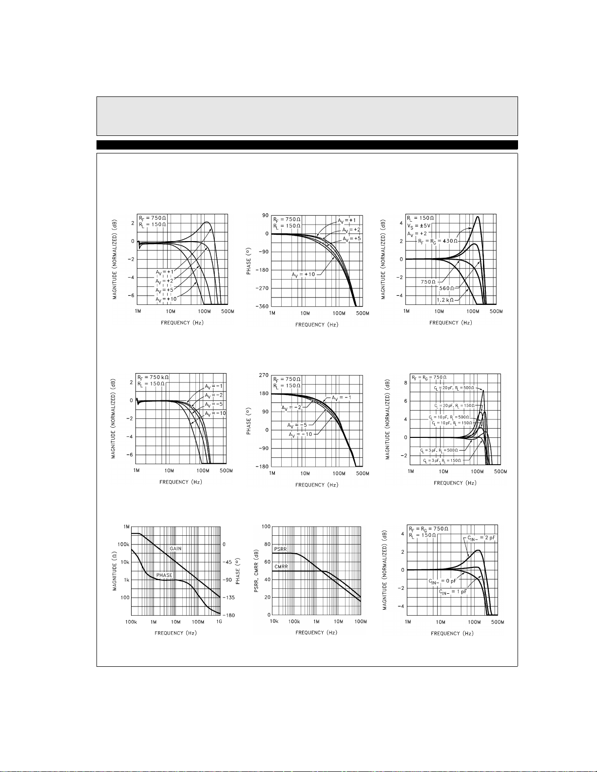
Typical Performance Curves
EL2180C/EL2280C/EL2480C-Preliminary
250MHz / 3mA Current Mode Feedback Amplifiers
Non-Inverting Frequency
Response (Gain)
(PDIP and SOIC Packages)
Inverting Frequency
Response (Gain)
(PDIP and SOIC Packages)
Non–Inverting Frequency
Response (Phase)
(PDIP and SOIC Packages)
Inverting Frequency
Response (Phase)
(PDIP and SOIC Packages)
Frequency Response
for Various RF and R
(PDIP and SOIC Packages)
Frequency Response
for Various RL and C
(PDIP and SOIC Packages)
G
L
Transimpedance (ROL) vs
Frequency
PSRR and CMRR
vs Frequency
5
Frequency Response for
Various CIN-
Page 6

EL2180C/EL2280C/EL2480C-Preliminary
250MHz / 3mA Current Mode Feedback Amplifiers
Typical Performance Curves
Voltage and Current
Noise vs Frequency
2nd and 3rd Harmonic
Distortion vs Frequency
Output Voltage
Swing vs Frequency
EL2180C/EL2280C/EL2480C-Preliminary
-3 dB Bandwidth and Peaking
vs Supply Voltage for
Various Non-Inverting Gains
-3 dB Bandwidth and Peaking
vs Supply Voltage for
Various Inverting Gains
Output Voltage Swing
vs Supply Voltage
Supply Current vs
Supply Voltage
Common-Mode Input Range
vs Supply Voltage
6
Slew Rate vs
Supply Voltage
Page 7

EL2180C/EL2280C/EL2480C-Preliminary
Typical Performance Curves
EL2180C/EL2280C/EL2480C-Preliminary
250MHz / 3mA Current Mode Feedback Amplifiers
Input Bias Current
vs Die Temperature
-3 dB Bandwidth and Peaking
vs Die Temperature for
Various Non-Inverting Gains
Short-Circuit Current
vs Die Temperature
-3 dB Bandwidth vs
Die Temperature for
Various Inverting Gains
Transimpedance (ROL)
vs Die Temperature
Input Offset Voltage
vs Die Temperature
Supply Current vs
Die Temperature
Input Voltage Range
vs Die Temperature
7
Slew Rate vs
Die Temperature
Page 8

EL2180C/EL2280C/EL2480C-Preliminary
250MHz / 3mA Current Mode Feedback Amplifiers
Typical Performance Curves
Differential Gain and
Phase vs DC Input
Voltage at 3.58 MHz
Differential Gain and
Phase vs DC Input
Voltage at 3.58 MHz
Settling Time vs
Settling Accuracy
EL2180C/EL2280C/EL2480C-Preliminary
Small-Signal Step Response Large-Signal Step Response
5-Lead Plastic SOT23
Maximum Power Dissipation
vs Ambient Temperature
8-Pin Plastic DIP
Maximum Power Dissipation
vs Ambient Temperature
8
8-Lead SO
Maximum Power Dissipation
vs Ambient Temperature
Page 9

EL2180C/EL2280C/EL2480C-Preliminary
Typical Performance Curves
EL2180C/EL2280C/EL2480C-Preliminary
250MHz / 3mA Current Mode Feedback Amplifiers
14-Pin Plastic DIP
Maximum Power Dissipation
vs Ambient Temperature
Non-Inverting Frequency
Response (Gain)
(SOT23-5 Package)
14-Lead SO
Maximum Power Dissipation
vs Ambient Temperature
Non-Inverting Frequency
Response (Phase)
(SOT23-5 Package)
Channel Separation
vs Frequency
Frequency Response for
Various RF and R
(SOT23-5 Package)
G
Inverting Frequency
Response (Gain)
(SOT23-5 Package)
Inverting Frequency
Response (Phase)
(SOT23-5 Package)
9
Page 10

EL2180C/EL2280C/EL2480C-Preliminary
250MHz / 3mA Current Mode Feedback Amplifiers
Applications Information
Product Description
The EL2180C/EL2280C/EL2480C are current-feedback
operational amplifiers that offer a wide -3dB bandwidth
of 250MHz and a low supply current of 3mA per amplifier. All of these products also feature high output
current drive. The EL2180C can output 100mA, while
the EL2280C and the EL2480C can output 55mA per
amplifier. The EL2180C/EL2280C/EL2480C work with
supply voltages ranging from a single 3V to ±6V and
they are also capable of swinging to within 1V of either
supply on the input and the output. Because of their cur-
EL2180C/EL2280C/EL2480C-Preliminary
rent-feedback topology, the EL2180C/EL2280C/
EL2480C do not have the normal gain-bandwidth product associated with voltage-feedback operational
amplifiers. This allows their -3dB bandwidth to remain
relatively constant as closed-loop gain is increased. This
combination of high bandwidth and low power, together
with aggressive pricing make the EL2180C/EL2280C/
EL2480C the ideal choice for many low-power/highbandwidth applications such as portable computing,
HDSL, and video processing.
For applications where board space is extremely critical,
the EL2180C is available in the tiny 5-pin SOT23 package, which has a footprint 28% the size of an 8-pin SO.
The EL2480C is available in the 24-pin LPP package,
offering board space savings and better power dissipation compared to the SO and PDIP packages. The
EL2180C/EL2280C/EL2480C are each also available in
industry-standard pinouts in PDIP and SO packages.
For single, dual, and triple applications with disable,
consider the EL2186C (8-pin single), EL2286C (14-pin
dual), and EL2386C (16-pin triple). If lower power is
required, refer to the EL2170C/EL2176C family which
provides singles, duals, and quads with 70MHz of bandwidth while consuming 1mA of supply current per
amplifier.
Power Supply Bypassing and Printed Circuit
Board Layout
As with any high-frequency device, good printed circuit
board layout is necessary for optimum performance.
Ground plane construction is highly recommended.
Lead lengths should be as short as possible. The power
supply pins must be well bypassed to reduce the risk of
oscillation. The combination of a 4.7µF tantalum capacitor in parallel with a 0.1µF capacitor has been shown to
work well when placed at each supply pin.
For good AC performance, parasitic capacitance should
be kept to a minimum especially at the inverting input
(see the Capacitance at the Inverting Input section).
Ground plane construction should be used, but it should
be removed from the area near the inverting input to
minimize any stray capacitance at that node. Carbon or
Metal-Film resistors are acceptable with the Metal-Film
resistors giving slightly less peaking and bandwidth
because of their additional series inductance. Use of
sockets, particularly for the SO package, should be
avoided if possible. Sockets add parasitic inductance and
capacitance which will result in some additional peaking
and overshoot.
Capacitance at the Inverting Input
Any manufacturer's high-speed voltage- or current-feedback amplifier can be affected by stray capacitance at
the inverting input. For inverting gains this parasitic
capacitance has little effect because the inverting input is
a virtual ground, but for non-inverting gains this capacitance (in conjunction with the feedback and gain
resistors) creates a pole in the feedback path of the
amplifier. This pole, if low enough in frequency, has the
same destabilizing effect as a zero in the forward openloop response. The use of large value feedback and gain
resistors further exacerbates the problem by further lowering the pole frequency.
The experienced user with a large amount of PC board
layout experience may find in rare cases that the
EL2180C/EL2280C/EL2480C have less bandwidth than
expected.
The reduction of feedback resistor values (or the addition of a very small amount of external capacitance at
the inverting input, e.g. 0.5pF) will increase bandwidth
as desired. Please see the curves for Frequency
Response for Various RF and RG, and Frequency
Response for Various CIN-.
10
Page 11

EL2180C/EL2280C/EL2480C-Preliminary
250MHz / 3mA Current Mode Feedback Amplifiers
EL2180C/EL2280C/EL2480C-Preliminary
Feedback Resistor Values
The EL2180C/EL2280C/EL2480C have been designed
and specified at gains of +1 and +2 with R
PDIP and SO packages and R
package. These values of feedback resistors give
250MHz of -3dB bandwidth at AV = +1 with about
2.5dB of peaking, and 180MHz of -3dB bandwidth at
AV = +2 with about 0.1dB of peaking. The 5-pin SOT23
package is characterized with a smaller value of feedback resistor, for a given bandwidth, to compensate for
lower parasitics within both the package itself and the
printed circuit board where it will be placed. Since the
EL2180C/EL2280C/EL2480C are current-feedback
amplifiers, it is also possible to change the value of RF to
get more bandwidth. As seen in the curve of Frequency
Response For Various RF and RG, bandwidth and peaking can be easily modified by varying the value of the
feedback resistor.
Because the EL2180C/EL2280C/EL2480C are currentfeedback amplifiers, their gain-bandwidth product is not
a constant for different closed-loop gains. This feature
actually allows the EL2180C/EL2280C/EL2480C to
maintain about the same -3dB bandwidth, regardless of
closed-loop gain. However, as closed-loop gain is
increased, bandwidth decreases slightly while stability
increases. Since the loop stability is improving with
higher closed-loop gains, it becomes possible to reduce
the value of R
still retain stability, resulting in only a slight loss of
bandwidth with increased closed-loop gain.
below the specified 560Ω and 750Ω and
F
= 560Ω in 5-pin SOT23
F
= 750Ω in
F
Supply Voltage Range and Single-Supply
Operation
The EL2180C/EL2280C/EL2480C have been designed
to operate with supply voltages having a span of greater
than 3V, and less than 12V. In practical terms, this
means that the EL2180C/EL2280C/EL2480C will operate on dual supplies ranging from ±1.5V to ±6V. With a
single-supply, the EL2180C/EL2280C/EL2480C will
operate from +3V to +12V.
As supply voltages continue to decrease, it becomes necessary to provide input and output voltage ranges that
can get as close as possible to the supply voltages. The
EL2180C/EL2280C/EL2480C have an input voltage
range that extends to within 1V of either supply. So, for
example, on a single +5V supply, the EL2180C/
EL2280C/EL2480C have an input range which spans
from 1V to 4V. The output range of the
EL2180C/EL2280C/EL2480C is also quite large,
extending to within 1V of the supply rail. On a ±5V supply, the output is therefore capable of swinging from----
-4V to +4V. Single-supply output range is even larger
because of the increased negative swing due to the external pull-down resistor to ground. On a single +5V
supply, output voltage range is about 0.3V to 4V.
Video Performance
For good video performance, an amplifier is required to
maintain the same output impedance and the same frequency response as DC levels are changed at the output.
This is especially difficult when driving a standard video
load of 150Ω, because of the change in output current
with DC level. Until the EL2180C/EL2280C/EL2480C,
good Differential Gain could only be achieved by running high idle currents through the output transistors (to
reduce variations in output impedance). These currents
were typically comparable to the entire 3mA supply current of each EL2180C/EL2280C/EL2480C amplifier!
Special circuitry has been incorporated in the
EL2180C/EL2280C/EL2480C to reduce the variation of
output impedance with current output. This results in dG
and dP specifications of 0.05% and 0.05° while driving
150Ω at a gain of +2.
Video Performance has also been measured with a 500Ω
load at a gain of +1. Under these conditions, the
EL2180C/EL2280C/EL2480C have dG and dP specifications of 0.01% and 0.01° respectively while driving
500Ω at A
= +1.
V
Output Drive Capability
In spite of its low 3mA of supply current, the EL2180C
is capable of providing a minimum of ±80mA of output
current. Similarly, each amplifier of the EL2280C and
the EL2480C is capable of providing a minimum of
±50mA. These output drive levels are unprecedented in
amplifiers running at these supply currents. With a minimum ±80mA of output drive, the EL2180C is capable
of driving 50Ω loads to ±4V, making it an excellent
choice for driving isolation transformers in telecommunications applications. Similarly, the ±50mA minimum
11
Page 12

EL2180C/EL2280C/EL2480C-Preliminary
250MHz / 3mA Current Mode Feedback Amplifiers
output drive of each EL2280C and EL2480C amplifier
allows swings of ±2.5V into 50Ω loads.
Driving Cables and Capacitive Loads
When used as a cable driver, double termination is
always recommended for reflection-free performance.
For those applications, the back-termination series resistor will decouple the EL2180C/EL2280C/EL2480C
from the cable and allow extensive capacitive drive.
However, other applications may have high capacitive
loads without a back-termination resistor. In these appli-
cations, a small series resistor (usually between 5Ω and
50Ω) can be placed in series with the output to eliminate
EL2180C/EL2280C/EL2480C-Preliminary
most peaking. The gain resistor (RG) can then be chosen
to make up for any gain loss which may be created by
this additional resistor at the output. In many cases it is
also possible to simply increase the value of the feedback resistor (RF) to reduce the peaking.
Current Limiting
The EL2180C/EL2280C/EL2480C have no internal current-limiting circuitry. If any output is shorted, it is
possible to exceed the Absolute Maximum Ratings for
output current or power dissipation, potentially resulting
in the destruction of the device.
Power Dissipation
With the high output drive capability of the
EL2180C/EL2280C/EL2480C, it is possible to exceed
the 150°C Absolute Maximum junction temperature
under certain very high load current conditions. Generally speaking, when R
important to calculate the maximum junction temperature (T
) for the application to determine if power-
JMAX
supply voltages, load conditions, or package type need
to be modified for the EL2180C/EL2280C/EL2480C to
remain in the safe operating area. These parameters are
calculated as follows:
falls below about 25Ω, it is
L
n = Number of Amplifiers in the Package
PD
= Maximum Power Dissipation of Each
MAX
Amplifier in the Package
PD
for each amplifier can be calculated as follows:
MAX
PD
MAX
2( V
SISMAX
) VS( V
OUTMAX
where:
VS = Supply Voltage
I
= Maximum Supply Current of 1 Amplifier
SMAX
V
OUTMAX
= Maximum Output Voltage of the
Application
RL = Load Resistance
)
V
OUTMAX
----------------------------×–+××=
R
L
T
JMAXTMAXΘJA
where:
T
= Maximum Ambient Temperature
MAX
θ
= Thermal Resistance of the Package
JA
nPD
××()+=
MAX
12
Page 13

EL2180C/EL2280C/EL2480C-Preliminary
Typical Application Circuits
250MHz / 3mA Current Mode Feedback Amplifiers
VS+
VS-
0.1µF
OUT
0.1µF
5Ω
+5V
IN+
EL2180C
IN-
-5V
750Ω
EL2180C/EL2280C/EL2480C-Preliminary
VS+
VS-
0.1µF
OUT
0.1µF
5Ω
+5V
IN+
EL2180C
IN-
-5V
V
IN
750Ω750Ω
V
OUT
Figure 1. Inverting 200mA Output Current Distribution Amplifier
750Ω750Ω
VS+
0.1µF
OUT
VS-
0.1µF
0.1µF
750Ω
750Ω
+5V
IN+
*see note
IN-
-5V
+5V
* Note:
½ EL2280C or
¼ EL2480C
V
IN
IN+
*see note
IN-
-5V
VS+
VS-
OUT
0.1µF
V
Figure 2. Fast-Settling Precision Amplifier
13
OUT
Page 14

EL2180C/EL2280C/EL2480C-Preliminary
250MHz / 3mA Current Mode Feedback Amplifiers
Typical Application Circuits (Continued)
VS+
VS-
VS+
VS-
0.1µF
OUT
0.1µF
0.1µF
OUT
0.1µF
120Ω
120Ω
+5V
IN+
*see note
*see note
IN-
V
+
OUT
-
OUT
0.1µF
1kΩ
240Ω
0.1µF
1kΩ
750Ω750Ω
750Ω750Ω
-5V
+5V
IN+
*see note
*see note
IN-
-5V
+5V
IN+
*see note
IN-
-5V
750Ω
EL2180C/EL2280C/EL2480C-Preliminary
+5V
IN+
*see note V
IN-
-5V
750Ω750Ω
* Note:
V
IN
EL2180 or
½ EL2280C or
¼ EL2480C
0.1µF
VS+
OUT
VS-
0.1µF
0.1µF
VS+
OUT V
VS-
0.1µF
RECEIVERTRANSMITTER
OUT
Figure 3. Differential Line Driver/Receiver
14
Page 15

EL2180C/EL2280C/EL2480C-Preliminary
250MHz / 3mA Current Mode Feedback Amplifiers
EL2180C/EL2280C/EL2480C Macromodel
* EL2180 Macromodel
* Revision A, March 1995
* AC characteristics used: Rf = Rg = 750 ohms
* Connections: +input
* | -input
* | | +Vsupply
* | | | -Vsupply
* | | | | output
* | | | | |
.subckt EL2180/el 3 2 7 4 6
*
* Input Stage
*
e1 10 0 3 0 1.0
vis 10 9 0V
h2 9 12 vxx 1.0
r1 2 11 400
l1 11 12 25nH
iinp 3 0 1.5uA
iinm 2 0 3uA
r12 3 0 2Meg
*
* Slew Rate Limiting
*
h1 13 0 vis 600
r2 13 14 1K
d1 14 0 dclamp
d2 0 14 dclamp
*
* High Frequency Pole
*
e2 30 0 14 0 0.00166666666
l3 30 17 150nH
c5 17 0 0.8pF
r5 17 0 165
*
* Transimpedance Stage
*
g1 0 18 17 0 1.0
rol 18 0 450K
cdp 18 0 0.675pF
*
* Output Stage
*
q1 4 18 19 qp
q2 7 18 20 qn
q3 7 19 21 qn
q4 4 20 22 qp
r7 21 6 4
r8 22 6 4
ios1 7 19 1mA
ios2 20 4 1mA
*
* Supply Current
*
ips 7 4 0.2mA
*
* Error Terms
*
ivos 0 23 0.2mA
vxx 23 0 0V
e4 24 0 3 0 1.0
EL2180C/EL2280C/EL2480C-Preliminary
15
Page 16

EL2180C/EL2280C/EL2480C-Preliminary
250MHz / 3mA Current Mode Feedback Amplifiers
e5 25 0 7 0 1.0
e6 26 0 4 0 -1.0
r9 24 23 316
r10 25 23 3.2K
r11 26 23 3.2K
*
* Models
*
.model qn npn(is=5e-15 bf=200 tf=0.01nS)
*.model qp pnp(is=5e-15 bf=200 tf=0.01nS)
.model dclamp d(is=1e-30 ibv=0.266
+ bv=0.71v n=4)
.ends
EL2180C/EL2280C/EL2480C-Preliminary
16
Page 17

EL2180C/EL2280C/EL2480C-Preliminary
250MHz / 3mA Current Mode Feedback Amplifiers
EL2180C/EL2280C/EL2480C-
General Disclaimer
Specifications contained in this data sheet are in effect as of the publication date shown. Elantec, Inc. reserves the right to make changes in the circuitry or specifications contained herein at any time without notice. Elantec, Inc. assumes no responsibility for the use of any circuits described
herein and makes no representations that they are free from patent infringement.
WARNING - Life Support Policy
Elantec, Inc. products are not authorized for and should not be used
within Life Support Systems without the specific written consent of
Elantec, Inc. Life Support systems are equipment intended to sup-
Elantec Semiconductor, Inc.
675 Trade Zone Blvd.
Milpitas, CA 95035
Telephone: (408) 945-1323
(888) ELANTEC
Fax: (408) 945-9305
European Office: +44-118-977-6020
Japan Technical Center: +81-45-682-5820
port or sustain life and whose failure to perform when properly used
in accordance with instructions provided can be reasonably
expected to result in significant personal injury or death. Users contemplating application of Elantec, Inc. Products in Life Support
Systems are requested to contact Elantec, Inc. factory headquarters
to establish suitable terms & conditions for these applications. Elantec, Inc.’s warranty is limited to replacement of defective
components and does not cover injury to persons or property or
other consequential damages.
July 19, 2001
17
Printed in U.S.A.
 Loading...