

Page 1
EL2257C/EL2357C
125 MHz Single Supply, Clamping Op Amps
EL2257C/EL2357C
Features
• Specified for +3V, +5V, or ± 5V
Applications
• Power Down to 0 µA
• Output Voltage Clamp
• Large Input Common Mode Range
0V < V
• Output Swings to Ground Without
Saturating
• -3 dB Bandwidth = 125 MHz
• ± 0.1 dB Bandwidth = 30 MHz
• Low Supply Current = 5 mA
• Slew Rate = 275 V/µs
• Low Offset Voltage = 4 mV max
• Output Current = ±100 mA
• High Open Loop Gain = 80 dB
• Differential Gain = 0.05%
• Differential Phase = 0.05°
< VS - 1.2V
CM
Applications
• Video Amplifier
• PCMCIA Applications
•A/D Driver
•Line Driver
• Portable Computers
• High Speed Communications
• RGB Printer, FAX, Scanner
Applications
• Broadcast Equi pment
• Active Filtering
• Multiplexing
General Description
The EL2257C/EL2357C are supply op amps. Prior si ngle supply op
amps have general ly been limite d to bandwid ths and slew rates 1/4
that of the EL2257C /EL2357C. The 125 MHz b andwidth, 2 75 V/µs
slew rate, and 0.05%/0.05° differential gain/differential phase makes
this part ideal for single or dual supply video speed applications. With
its voltage feedback architecture, this amplifier can accept reactive
feedback networks, allowing them to be used in analog filtering applications. The inputs can sense signals below the bo ttom supp ly rail and
as high as 1.2V below the top rail. Connecting the load resistor to
ground and operating fr om a single supply, the output s swing completely to ground without saturating. The outputs can also drive to
within 1.2V of the top rail. The EL2257C/EL2357C will output
±100 mA and will operate with single supply voltages as low as 2.7V,
making them ideal for portable, low power applications.
The EL2257C/EL2357C have a high speed disable feature. Applying a
low logic level to all ENABLE pin s redu ces the supply current to 0 µA
within 50 ns. Each amplifier has its own ENABLE pin. This is useful
for both multiplexing and reducing power consumption.
The EL2257C/EL2357C also hav e an output v oltage clamp feature.
This clamp is a fast recovery (<7 ns) output clamp that pr events the
output voltage from going above the preset clamp voltage. This feature
is desirable for A/D applications, as A/D converters can require long
times to recover if overdriven.
The EL2257C/EL2357C are available in plastic DIP and SOIC packages. Both parts operate over the industrial temperature range of -40°C
to +85°C. For single amplifier applications, see the
EL2150C/EL2157C. For space saving, industry standard pin out dual
and quad applications , see the EL2250C/EL2450C.
Ordering Information
Part No. Temp. Range Package Outline #
EL2257CN -40°C to +85 °C 14 Pin PDIP MDP0031 EL2257CS -40°C to +85°C 14 Pin SOIC MDP0027 EL2357CN -40°C to +85°C 16 Pin PDIP MDP0031 EL2357CS -40°C to +85°C 16 Pin SOIC MDP0027
© 1995 Elantec, Inc.
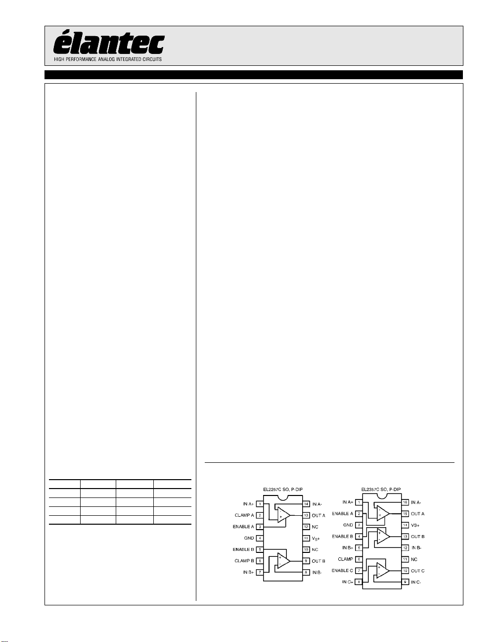
Connection Diagrams
Top View
January 5, 2000
Top View
Page 2
EL2257C/EL2357C
125 MHz Single Supply, Clamping Op Amps
Absolute Maximum Ratings (T
Supply Voltage between VS and GND 12.6V
Input V oltage (IN+, IN-, EN ABLE, CLAMP) GND–0.3V, V
EL2257C/EL2357C
Differential Input Voltage ±6V
Maximum Output Current 90 mA
Output Short Circuit Duration (see note
[1]
DC Electrical Characteristics)
= 25 °C)
A
+0.3V
S
Power Dissipation See Curves
Storage Temperature Range -65°C to +150°C
Ambient Operating Temperature Range -40°C to +85°C
Operating Junction Temperature 150°C
Important Note:
All parameters having Min/Max specifications are guaranteed. The Test Level column indicates the specific device testing actually performed during
production and Quality inspection. Elantec performs most electrical tests using modern high-speed automatic test equipment, specifically the LTX77
Series system. Unless otherwise noted, all tests are pulsed tests, therefor T
= TC = TA.
J
Test Level Test Procedure
I 100% production tested and QA sample tested per QA test plan QCX0002.
II 100% production tested at T
= 25°C and QA sample tested at TA = 25°C, T
A
MAX
and T
per QA test plan QCX0002.
MIN
III QA sample tested per QA test plan QCX0002.
IV Parameter is guaranteed (but not tested) by Design and Characterization Data.
V Parameter is typical value at T
= 25°C for information purposes only.
A
DC Electrical Characteristics
VS=+5V, GND=0V, TA=25°C, VCM=1.5V, V
Parameter Description Test Conditions Min Typ Max
V
OS
TCV
Offset Voltage EL2257C -4 4 I mV
Offset Voltage Temperature Coefficient Measured from Tmin to Tmax 10 V µV/°C
OS
IB Input Bias Current V
I
OS
TCI
Input Offset Current VIN=0V -1100 150 +1100 I nA Input Bias Current Temperature Coefficient Measured from Tmin to Tmax 50 V nA/°C
OS
PSRR Power Supply Rejection Ratio V
CMRR Common Mode Rejection Ratio VCM=0V to +3.8V 50 65 I dB
CMIR Common Mode Input Range 0 V
R
C
R
I
S,ON
I
S,OFF
IN
IN
OUT
Input Resistance Common Mode 1 2 I MΩ
Input Capacitance SOIC Package 1 V pF
Output Resistance Av=+1 40 V mΩ
Supply Current - Enabled (per amplifier) VS=V
Supply Current - Shut Down (per amplifier) VS=V
PSOR Power Supply Operating Range 2.7 12.0 I V AVOL Open Loop Gain V
OUT
=1.5V, V
CLAMP
=+5V, V
=+5V, unless otherwise specified.
ENABLE
Test
Level Units
EL2357C -6 6 I mV
=0V -5.5 -10 I µA
IN
S=VENABLE
V
CLAMP
=+2.7V to +12V,
=OPEN
45 70 I dB
VCM=0V to +3.0V 55 70 I dB
-1.2 I V
S
PDIP Package 1.5 V pF
=+12V, V
CLAMP
=+10V, V
CLAMP
V
R
V
V
=+12V, V
S=VCLAMP
=+12V, V
S=VCLAMP
=1 kΩ to GND
L
=+1.5V to +3.5V, RL=1 kΩ to GND 70 V dB
OUT
=+1.5V to +3.5V, RL=150Ω to GND 60 V dB
OUT
=+12V 5 6.5 I mA
ENABLE
=+0.5V 0 50 I µA
ENABLE
=+0.5V 5 V µA
ENABLE
=+2V to +9V,
OUT
65 80 I dB
2
Page 3
EL2257C/EL2357C
125 MHz Single Supply, Clamping Op Amps
DC Electrical Characteristics (Continued)
VS=+5V, GND=0V, TA=25°C, VCM=1.5V, V
Parameter Description Test Conditions Min Typ Max
V
OP
V
ON
I
OUT
I
OUT,OFF
V
IH-EN
V
IL-EN
I
IH-EN
I
IL-EN
V
OR-CL
V
ACC-CL
I
IH-CL
I
IL-CL
Positive Output Voltage Swing VS=+12V, AV=+1, RL=1 kΩ to 0V 10.8 V V
Negative Output Voltage Swing VS=+12V, AV=+1, RL=150Ω to 0V 5.5 8 I mV
Output Current
[1]
Output Current, Disabled V
ENABLE pin Voltage for Power Up Relative to GND Pin 2.0 I V
ENABLE pin Voltage for Shut Down Relative to GND Pin 0.5 I V
ENABLE pin Input Current-High
ENABLE pin Input Current-Low
Voltage Clamp Operating Range
CLAMP Accuracy
[4]
CLAMP pin Input Current - High VS=V
CLAMP pin Input Current - Low / Per
Amplifier
1. Internal short circuit protection circuitry has been built into the EL2257C/EL2357C. See the Applications section.
2. If the disable feature is not desired, tie the ENABLE pins to the V
3. The maximum output voltage that can be clamped is limited to the maximum positive output Voltage, or V
inactivates the clamp. If the clamp feature is not desired, either tie the CLAMP pin to the V
4. The clamp accuracy is affected by V
OUT
=1.5V, V
=+5V, V
CLAMP
V
=+12V, AV=+1, RL=150Ω to 0V 9.6 10.0 I V
S
=±5V, AV=+1, RL=1 kΩ to 0V 4.0 V V
V
S
=±5V, AV=+1, RL=150Ω to 0V 3.4 3.8 I V
V
S
V
=+3V, AV=+1, RL=150Ω to 0V 1.8 1.95 I V
S
=±5V, AV=+1, RL=1 kΩ to 0V -4.0 V V
V
S
V
=±5V, AV=+1, RL=150Ω to 0V -3.7 -3.4 I V
S
=+5V, unless otherwise specified.
ENABLE
VS=±5V, AV=+1, RL=10Ω to 0V ±75 ±100 I mA
=±5V, AV=+1, RL=50Ω to 0V ±60 V mA
V
S
=+0.5V 0 20 I µA
ENABLE
[2]
[2]
[3]
and RL. See the Typical Curves Section and the Clamp Accuracy vs. VIN and RL curve.
IN
VS=V
VS=V
CLAMP
CLAMP
=+12V, V
=+12V, V
=+12V 340 410 I µA
ENABLE
=+0.5V 0 1 I µA
ENABLE
Relative to GND Pin 1.2 V
VIN=+4V, RL=1 kΩ to GND
=+1.5V and +3.5V
V
CLAMP
=+12V 12 25 I µA
CLAMP
VS=+12V, V
S
=+1.2V -30 -15 I µA
CLAMP
pin, or apply a logic high level to the ENABLE pins.
pin, or simply let the CLAMP pin float.
S
-250 100 250 I mV
. Applying a Voltage higher than VOP
OP
OP
EL2257C/EL2357C
Test
Level Units
IV
3
Page 4
EL2257C/EL2357C
125 MHz Single Supply, Clamping Op Amps
Closed Loop AC Electrical Characteristics
VS=+5V, GND=0V, TA=25°C, VCM=+1.5V, V
unless otherwise specified
EL2257C/EL2357C
[1]
Parameter Description Test Conditions Min Typ Max
BW -3 dB Bandwidth (Vout=400 mVp-p) V
BW ±0.1 dB Bandwidth (Vout=400 mVp-p) V
GBWP Gain Bandwidth Product V
PM Phase Margin R
SR Slew Rate V
t
R,tF
Rise Time, Fall Time ±0.1V Step 2.8 V ns
OS Overshoot ±0.1V Step 10 V %
t
PD
t
S
Propagation Delay ±0.1V step 3.2 V ns
0.1% Settling Time VS=±5V, RL=500Ω, AV=+1, V
0.01% Settling Time V
dG Differential Gain
dP Differential Phase
e
N
i
N
t
DIS
t
EN
t
CL
Input Noise Voltage f=10 kHz 48 V nV/ÐH
Input Noise Current f=10 kHz 1.25 V pA/ÐH
Disable Time
Enable Time
Clamp Overload Recovery 7Vns
[2]
[2]
[3]
[3]
1. All AC tests are performed on a “warmed up” part, except slew rate, which is pulse tested.
2. Standard NTSC signal = 286 mVp-p, f=3.58 MHz, as V
3. Disable/Enable time is defined as the time from when the logic signal is applied to the ENABLE pin to when the supply current has reached half its
final value.
OUT
=+1.5V, V
CLAMP
=+5V, V
=+5V, AV=+1, RF=0Ω, RL=150Ω to GND pin,
ENABLE
Test
Level Units
=+5V, AV=+1, RF=0Ω 125 V MHz
S
V
=+5V, AV=-1, RF=500Ω 60 V MHz
S
V
=+5V, AV=+2, RF=500Ω 60 V MHz
S
=+5V, AV=+10, RF=500Ω 6VMHz
V
S
V
=+12V, AV=+1, RF=0Ω 150 V MHz
S
V
=+3V, AV=+1, RF=0Ω 100 V MHz
S
=+12V, AV=+1, RF=0Ω 25 V MHz
S
V
=+5V, AV=+1, RF=0Ω 30 V MHz
S
V
=+3V, AV=+1, RF=0Ω 20 V MHz
S
=+12V, @ AV=+10 60 V MHz
S
=1 kΩ, CL=6 pF 55 V °
L
=+10V, RL=150Ω, Vout=0V to +6V 200 275 I V/µs
S
=+5V, RL=150Ω, Vout=0V to +3V 300 V V/µs
V
S
=±3V 40 V ns
=±5V, RL=500Ω, AV=+1, V
S
OUT
=±3V 75 V ns
OUT
AV=+2, RF=1 kΩ 0.05 V % AV=+2, RF=1 kΩ 0.05 V °
50 V ns
25 V ns
is swept from 0.6V to 1.314V. RL is DC coupled.
IN
z
z
4
Page 5
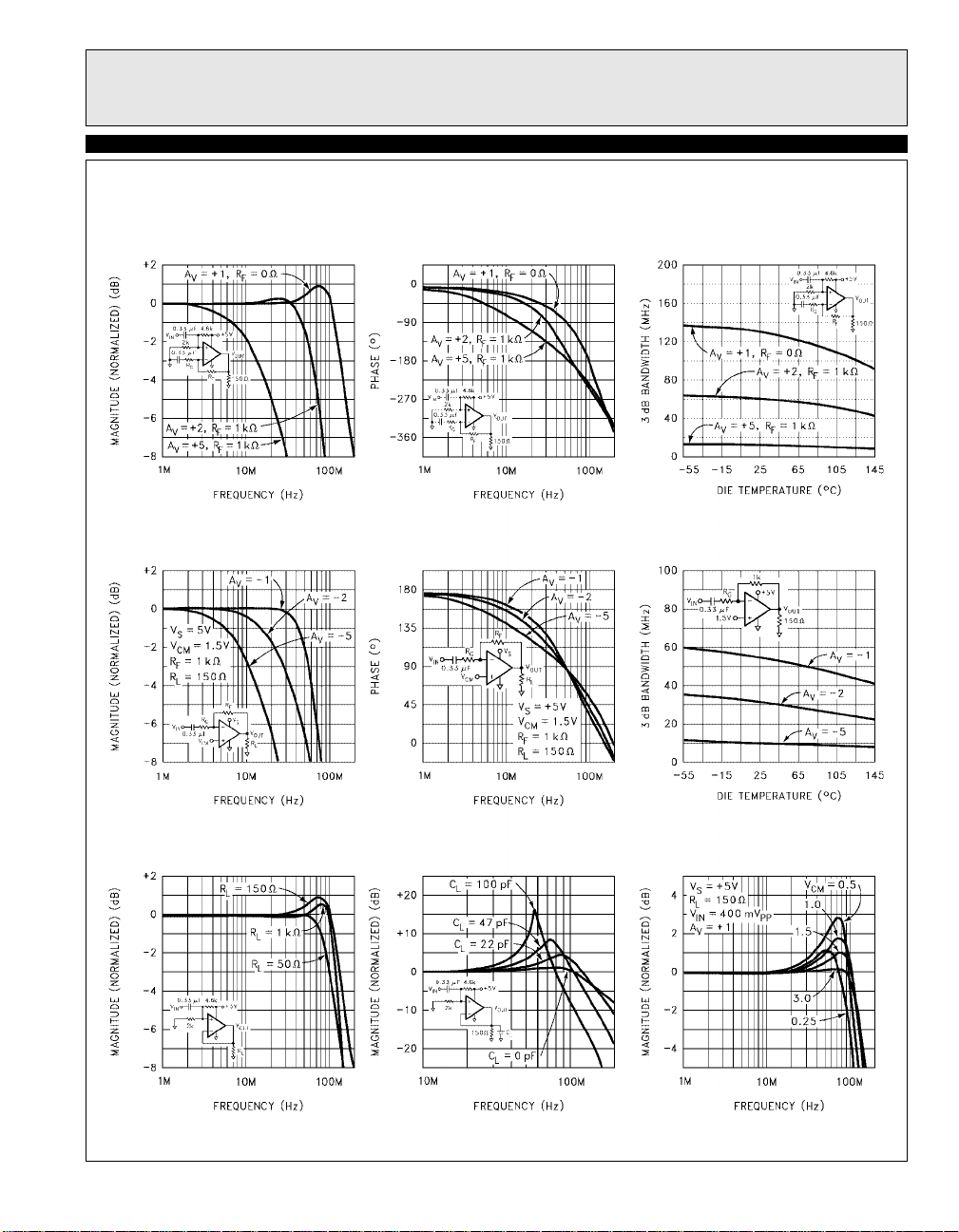
Typical Performance Curves
Non-Inverting
Frequency Response (Gain)
Inverting Frequency
Response (Gain)
125 MHz Single Supply, Clamping Op Amps
Non-Inverting
Frequency Response (Phase)
Inverting Frequency
Response (Phase)
EL2257C/EL2357C
3 dB Bandwidth vs
Temperature for
Non-Inverting Gains
3 dB Bandwidth vs
Temperature for
Inverting Gains
EL2257C/EL2357C
Frequency Response
for Various R
L
Frequency Response
for Various C
L
5
Non-Inverting
Frequency Response vs
Common Mode Voltage
Page 6
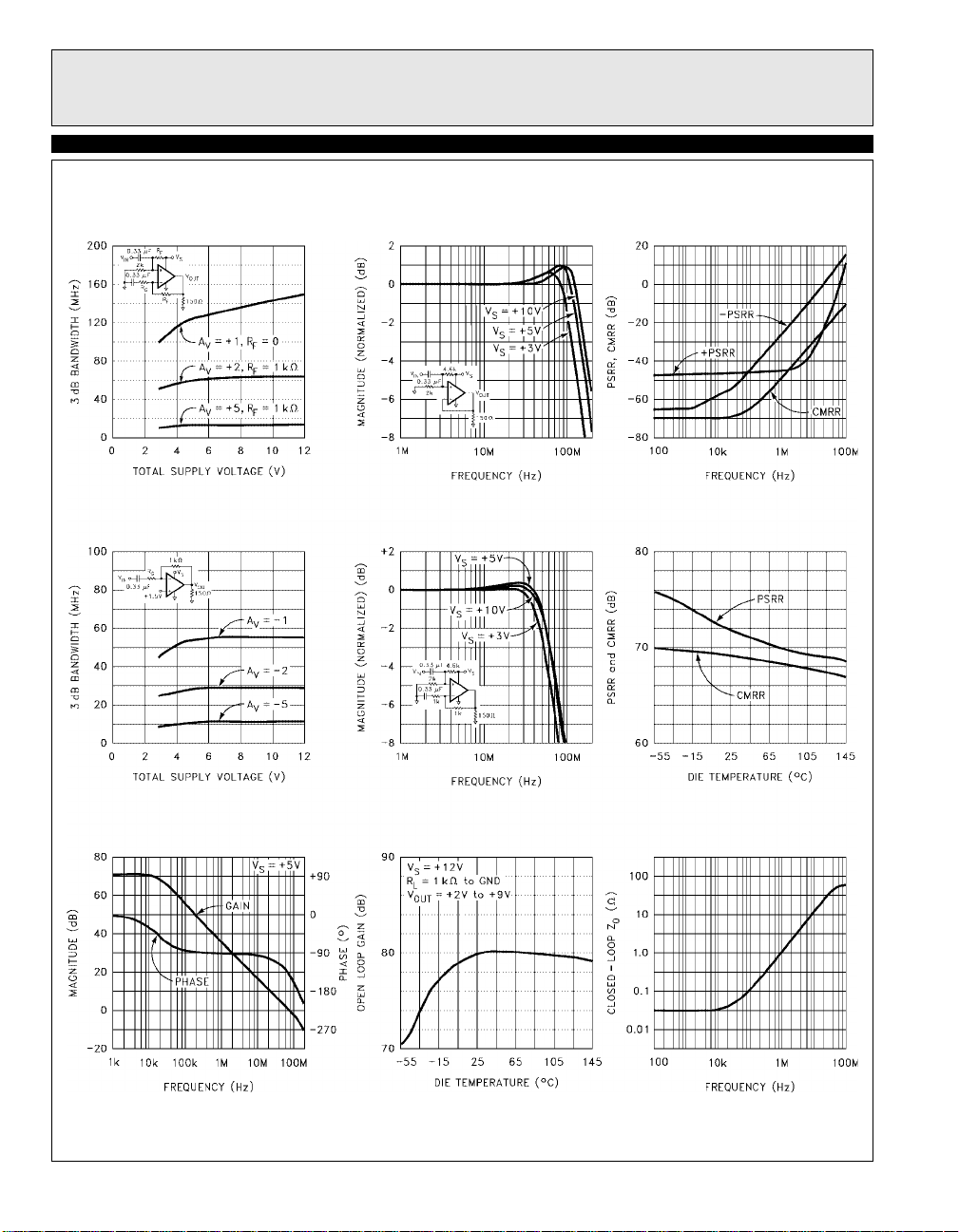
EL2257C/EL2357C
125 MHz Single Supply, Clamping Op Amps
EL2257C/EL2357C
3 dB Bandwidth vs
Supply Voltage for
Non-Inverting Gains
3 dB Bandwidth vs Supply
Voltage for Inverting Gains
Frequency Response for
Various Supply Voltages,
A
= + 1
V
Frequency Response for
Various Supply Voltages,
= + 2
A
V
PSSR and CMRR
vs Frequency
PSRR and CMRR vs
Die Temperature
Open Loop Gain and
Phase vs Frequency
Open Loop Voltage Gain
vs Die Temperature
6
Closed Loop Output
Impedance vs Frequency
Page 7
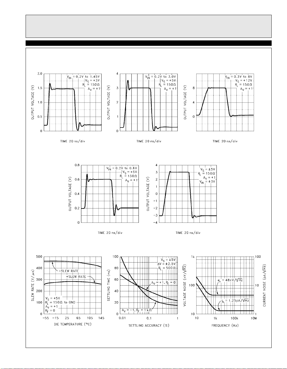
EL2257C/EL2357C
125 MHz Single Supply, Clamping Op Amps
EL2257C/EL2357C
Large Signal Step Response,
V
= +3V
S
Small Signal Step Response
Large Signal Step Response,
VS = +5V
Large Signal Step Response,
= ±5V
V
S
Large Signal Step Response,
VS = +12V
Slew Rate vs Temperature
Settling Time vs
Settling Accuracy
Voltage and Current Noise
vs Frequency
7
Page 8

EL2257C/EL2357C
125 MHz Single Supply, Clamping Op Amps
EL2257C/EL2357C
Differential Gai n fo r
Single Supply Operation
2nd and 3rd Harmonic
Distortion vs Frequency
Differential Phase for
Single Supply Operation
2nd and 3rd Harmonic
Distortion vs Frequency
Differential Gain and Phase
for Dual Supply Operation
2nd and 3rd Harmonic
Distortion vs Frequency
Output Voltage Swing vs
Frequency for THD < 0.1%
Output Voltage Swing vs
Frequency for Unlimited
Distortion
8
Output Current
vs Die Temperature
Page 9

EL2257C/EL2357C
125 MHz Single Supply, Clamping Op Amps
EL2257C/EL2357C
Supply Current vs
Supply Voltage
(per amplifier)
Offset Voltage vs
Die Temperature (4 Samples)
Supply Current vs
Die Temperature
(per amplifier)
Input Bias Cur r ent
vs Input Voltage
Input Resistance vs
Die Temperature
Input Offset Current
and Input Bias Current
vs Die Temperature
Positive Output Voltage
Swing vs Die Temperature,
RL = 150Ω to GND
Negative Output Voltage
Swing vs Die Temperature,
RL = 150Ω to GND
9
Clamp Accuracy
vs Die Temperature
Page 10

EL2257C/EL2357C
125 MHz Single Supply, Clamping Op Amps
EL2257C/EL2357C
IClamp Accuracy
R
= 150Ω
L
Enable Resp onse for a
Family of DC Inputs
Clamp Accuracy
RL = 1 kΩ
Disable Response for a
Family of DC Inputs
Clamp Accuracy
RL = 10 kΩ
Disable/Enable Response for a
Family of Sine Waves
OFF Isolation
10
Page 11

EL2257C/EL2357C
125 MHz Single Supply, Clamping Op Amps
EL2257C/EL2357C
EL2257
Channel to Channel
Isolation vs Frequency
14-Lead Plastic DIP
Maximum Power Dissipation
vs Ambient Temperature
EL2357
Channel to Channel
Isolation vs Frequency
16-Lead Plastic SO
Maximum Power Dissipation
vs Ambient Temperature
14-Lead Plastic SO
Maximum Power Dissipation
vs Ambient Temperature
16-Lead Plastic DIP
Maximum Power Dissipation
vs Ambient Temperature
11
Page 12

EL2257C/EL2357C
125 MHz Single Supply, Clamping Op Amps
Simplified Schematic (One Channel)
EL2257C/EL2357C
12
Page 13

Applications Information
EL2257C/EL2357C
EL2257C/EL2357C
125 MHz Single Supply, Clamping Op Amps
Product Description
The EL2257C/EL2357C’s, connected in voltage fol-
lower mode, -3 dB bandwidth is 125 MHz while
maintaining a 275 V/µs slew rate. Wit h an input a nd output common mode ra nge that include s ground, thes e
amplifiers were optimized for single supply operation,
but will also accept dual supplies. They operate on a
total supply voltage range as low as +2.7V or up to
+12V. This makes them ideal for +3V applications,
especially portable computers.
While many amplifiers claim to operate on a single supply, and some can sense ground at their inputs, most fail
to truly drive their outputs to gro und. If they do succeed
in driving to ground, the amplifier often saturates, causing distortion and recovery delays. However , special
circuitry built into the EL2257C/EL2357C allows the
output to follow the input signal to ground without
recovery delays.
Power Supply Bypassing And Printed Circuit
Board Layout
As with any high-frequency device, good printed circuit
board layout is necessary for optimum performance.
Ground plane constructio n is highly recommended.
Lead lengths should be as short as possible. The power
supply pins must be well bypassed to reduce the risk of
oscillation. The combi nation o f a 4.7 µF tantalum capacitor in parallel with a 0.1 µF ceramic capacitor has been
shown to work well when placed at each supply pin. For
single supply operation, where the GND pin is connected to the ground plane, a single 4.7 µF tantalum
capacitor in parallel with a 0.1 µF ceramic capacitor
from the V
For good AC performance, parasiti c capacita nce should
be kept to a minimum. Ground plane construction
should be used. Carbon or Metal-Film resistors a re
acceptable with the Metal-Film resistors giving slightly
less peaking and bandwidth because of their additional
series inductance. Use of sockets, particularly for the SO
package should b e avoi ded if possi ble. Soc kets add parasitic inductance and capacitance which will result in
some additional peaking and ove rsho ot.
pin to the GND pin will suffice.
S+
Supply Voltage Range and Single-Supply
Operation
The EL2257C/EL2357C have been designed to operate
with supply voltages ha vi ng a span of greater tha n 2. 7V,
and less than 12V. In practical terms, this means that the
EL2257C/EL2357C will operate on dual supplies ranging from ±1.35V to ±6V. With a single- supply, the
EL2257C/EL2357C will operat e from +2.7V to +12V.
Performance has been optimized f or a single +5V
supply.
Pins 11 and 4 (14 and 3) are the power supply pins on
the EL2257C (EL2357C). The positive power supply is
connected to pin 11 (14). When used in single supply
mode, pin 4 (3) is connected to ground. When used in
dual supply mode, the negati ve power supply is connected to pin 4 (3).
As supply voltages continue to decrease , it becomes necessary to provide input and output voltage ranges that
can get as close as possible to the supply voltages. The
EL2257C/EL2357C ha ve an input voltage rang e that
includes the negative supply and extends to within 1.2V
of the positive suppl y . So, for e xam pl e, on a si ngle +5V
supply, the EL2257C/EL2357C have an input range
which spans from 0V to 3.8V.
The output range o f the EL 22 57C/EL 2357 C is a lso q uite
large. It includes the negative rail, and extends to within
1V of the top supply rail with a 1 kΩ load. On a +5V
supply, the output is therefore capable of swi nging from
0V to +4V. On split supplies, t he outp ut will swing ±4V.
If the load resistor is tied to the negative rail and split
supplies are used, the output range is extended to the
negative rail.
Choice Of Feedback Resistor, R
The feedback resistor forms a pole with the input capacitance. As this pole becomes larger, phase margin is
reduced. This increases ringing in the time domain and
peaking in the frequency domain. Therefore, R
some maximum value which should not be exceeded for
optimum performance. If a large value of R
used, a small capacitor in the few picofarad range in parallel with RF can help to reduce this ringin g a nd pe a king
at the expense of reducing the bandwidth.
F
has
F
must be
F
13
Page 14

EL2257C/EL2357C
125 MHz Single Supply, Clamping Op Amps
As far as the output stage of the amplifier is concerned,
+ RG appear in parallel with RL for gains other than
R
F
+1. As this combination gets smaller, the bandwidth
EL2257C/EL2357C
falls off. Consequently, R
should not be exceeded for op timum performance.
= +1, RF = 0Ω is optimum. For AV = -1 or +2
For A
V
(noise gain of 2), optimu m r esponse is obt ain ed wit h R
between 500Ω and 1 kΩ. For AV = -4 or +5 (noise gain
of 5), keep R
between 2 kΩ and 10 kΩ.
F
has a minimum value that
F
Video Performance
For good video performance, an amplifier is required to
maintain the same output impedance and the same frequency response as DC level s are changed at the output.
This can be difficul t when d riv ing a stan dar d vide o load
of 150Ω, because of the change in output curre nt with
DC level. Differential Gain and Differential Phase for
the EL2257C/EL2357C are specified with the black
level of the output vide o signal se t to +1.2V. This al lows
ample room for the sync pulse even in a ga in of +2 con figuration. This results in dG and dP specifications of
0.05% and 0.05° while driving 150Ω at a gain of +2.
Setting the black level to other values, although acceptable, will compromise peak performance. For example,
looking at the single supply dG and dP curves for
=150Ω, if the output black level clamp is reduced
R
L
from 1.2V to 0.6V dG/dP will increase from
0.05%/0.05° to 0.08%/0.25°. Note that in a gain of +2
configuration, this is the lowest black leve l allowed such
that the sync tip doesn’t go below 0V.
If your application requires that the output goes to
ground, then the output stage of the EL2257C/EL2357C,
like all other single supply op amps, requires an external
pull down resistor tied to ground. As mentioned above,
the current flowing through this resistor become s the DC
bias current for the output st age NPN tran sistor. As this
current approaches zero, the NPN turns off, and dG and
dP will increase. This becomes more critical as the load
resistor is increased in value. While driving a light load,
such as 1 kΩ, if the input black level is kept above
1.25V, dG and dP are a respectable 0.03% and 0.03°.
For other biasing conditions see the Differential Gain
and Differential Phase vs. Input Voltage curves.
Output Drive Capability
In spite of their moderately low 5 mA of supply current,
the EL2257C/EL2357C are capable o f providing ±100
mA of output current into a 10Ω l oad, or ±60 mA into
50Ω. With this large output current capability, a 50Ω
load can be driven to ±3V with V
excellent choice for driving isolation transformers in
F
telecommunications applications.
= ±5V, making it an
S
Driving Cables and Capacitive Loads
When used as a cable driver, double termination is
always recommended for reflection-free perfor mance.
For those applications, the back-te rm ina ti on series re sistor will de-coup le the EL2257C/E L2357C from the
cable and allow extensive capacitive drive. Howe ver,
other applications may have high capacitive loads without a back-termination resistor. In these applications, a
small series resistor (usually between 5Ω and 50Ω) can
be placed in series with th e output to eliminate most
peaking. The gain resistor (R
make up for any gain loss which may be created by this
additional resistor at the output.
) can then be chosen to
G
Disable/Power-Down
Each amplifier in the EL2257 C/EL2357C can be ind ividually disabled, placing each output in a highimpedance state. The dis able or enable action takes only
about 40 ns. When all amplifiers are disabled, the total
supply current is reduced to 0 mA, thereby eliminating
all power consumption by the EL2257C/EL2357C. The
EL2257C/EL2357C amplifier’s power down can be
controlled by st andard CMOS sign al levels at ea ch
ENABLE pin. The applied CMOS signal is relative to
the GND pin. For example, if a single +5V supply is
used, the logic voltage levels will be +0.5V and +2.0V.
If using dual ±5V supplies, the logic leve ls will be -4.5V
and -3.0V. Letting all ENABLE pin s float will disable
the EL2257C/EL2357C. If the power-down feature is
not desired, connect all ENABLE pins to th e V
The guaranteed logic leve ls of +0 .5V an d +2. 0V are no t
standard TTL levels of +0.8V and +2.0V, so care must
be taken if standard TTL will be used to drive the
ENABLE pins.
S+
pin.
14
Page 15

Output Voltage Clamp
The EL2257C/EL2357C amplifiers have an output voltage clamp. This clamping acti on is fast, bei ng act ivated
almost instantaneously, and being deactivated in < 7 ns,
and prevents the output voltage from going above the
preset clamp voltage. This can be very helpful when the
EL2257C/EL2357C are used to drive an A/D converter,
as some converters can require long times to recover if
overdriven. The output voltag e remains at the clamp
voltage level as long as the product of the input voltage
and the gain setting exceeds the clamp voltage. For
example, if the EL2257C/EL2357C is connected in a
gain of 2, and +3V DC is appl ied to the CLAM P pin, an y
voltage higher than +1.5V at the inputs will be clamped
and +3V will be seen at the output. Each amplifier of the
EL2257C have their own CLAMP pin, so individual
clamp levels may be set, whereas a single CLAMP pin
controls the cl amp level of the EL2357C .
Figure 1 below is the EL2257C with each amplifier
unity gain connected. Amplifie r A is b eing d rive n by a 3
Vp-p sinewave and has 2.25V applied to CLAMPA,
while amplifier B is driven by a 3 Vp-p triangle wave
and 1.5V is applied to CLAMPB. The resulti ng output
waveforms, with their outputs being clamped is shown
in Figure 2.
EL2257C/EL2357C
EL2257C/EL2357C
125 MHz Single Supply, Clamping Op Amps
Figure 2.
Figure 3 shows the output of amplifier A of the same
circuit being driven by a 0.5V to 2.75V square wave as
the clamp voltage is varied from 1.0V to 2.5V, as well as
the unclamped output signa l. The risi ng edge of the signal is clamped to the vol tage ap plied to th e CLAMP pin
almost instantaneously. The output recovers from the
clamped mode with in 5–7 ns, depending on the clamp
voltage. Even when the CLAMP pin is taken 0.2V below
the minimum 1.2V specified, the output is still clamped
and recovers in about 11 ns.
Figure 1.
Figure 3.
The clamp accuracy is affected by 1) the CLAMP pin
voltage, 2) the input voltage, and 3) the load resistor.
Depending upon the application, the accuracy may be as
little as a few tens of millivolts up to a few hundred millivolts. Be sure to allow for these inaccuracies when
choosing the clamp vo ltage. Curves of Clam p A ccu racy
vs. V
the Typical Performance Curves Section.
15
and VIN for 3 values of RL are included in
CLAMP
Page 16

EL2257C/EL2357C
125 MHz Single Supply, Clamping Op Amps
Unlike amplifiers that clamp at the input and are therefore limited to non-inverting applications only, the
EL2257C/EL2357C outp ut cl am p arc hite ctur e work s f or
EL2257C/EL2357C
both inverting and non-inverting gain applications.
There is also no maximum voltage difference limitation
between V
clamped architectures.
The voltage clamp operates for any voltage between
+1.2V above the GND pin, and the minimum o utput
voltage swing, V
below +1.2V can saturate transistors and should therefore be avoided. Forcing the CLAMP pin abov e V
simply de-activates the CLAMP feature. In other words,
one cannot expect to clamp any voltage higher than what
the EL2257C/EL2357C can drive to in the first p lace. If
the clamp feature is not desired, either let the CLAMP
pin float or connect it to the VS+ pin.
and V
IN
OP
which is common on input
CLAMP
. Forcing the CLAMP pin much
EL2257C/EL2357C Comparator Application
The EL2257C/EL2357C can be used as a very fast, single supply comparator by utilizing the clamp feature.
Most op amps used as comparators allow only slow
speed operation because of output saturation issues.
However, by applying a DC voltage to the CLAMP pin
of the EL2257C/EL2 357 C, the ma xim um outpu t volta ge
can be clamped, thus preventing saturation. Figure 4 is
amplifier A of an EL22 57C i mpl eme nted as a co mpar ator. 2.25V DC is applied to the CLAMP pin, as well as
the IN- pin. A differential signal is then applied between
the inputs. Figure 5 shows the output square wave that
results when a ±1V, 10 MHz triangular wave is applied,
while Figure 6 is a graph of propag at io n de lay vs. ove rdrive as a square wave is presented at t he input.
OP
Figure 4.
Figure 5.
Propagation Delay vs Overdrive
EL2257/EL2357 as a Comparator
Figure 6.
16
Page 17

EL2257C/EL2357C
125 MHz Single Supply, Clamping Op Amps
EL2257C/EL2357C
Video Sync Pulse Remover Application
All CMOS Analog to Digital Converters (A/Ds) have a
parasitic latch-up problem when subjected to negative
input voltage levels. Since the sync tip contains no useful video information and it is a negative go ing pulse, we
can chop it off. Figure 7 shows a unity gain connected
amplifier A of an EL2257C. Figure 8 shows the complete input video signal applied at the input, as well as
the output signal with the negative going sync pulse
removed.
Figure 7.
inputs. Logic signals are applied to each of the ENABLE
pins to cycle through turning each of the amplifiers on,
one at a time. Figure 10 shows the resulting output
waveform at V
ns. Notice the outputs are tied directly together. Decoupling resistors at each output are not necessary. In fact,
adding them approximately doubles the switching time
to 100 ns.
. Switching is complete in about 50
OUT
Figure 9.
Figure 8.
Multiplexing with the EL2257C/EL2357C
The ENABLE pins on the EL2257C/EL2 35 7C a llo w for
multiplexing applications. Figure 9 shows an EL2357C
with all 3 outputs tied together, driving a back terminated 75Ω video load. Three sinewaves of varying
amplitudes and frequencies are app lied to the three
Figure 10.
Short Circuit Current Limit
The EL2257C/EL2357C have internal short circuit protection circuitry that protect it in the event of its output
being shorted to either supply rail. This limit is set to
around 100 mA nominally and reduces with increasing
junction temperature. It is intended to handle temporary
shorts. If an output is shorted indefinitely, the power dissipation could easily increase such that the part will be
destroyed. Maximum reliability is maintained if the output current never exceeds ±90 mA. A heat sink may be
17
Page 18

EL2257C/EL2357C
125 MHz Single Supply, Clamping Op Amps
required to keep the junction temperature below absolute maximum when an output is shorted indefinite ly.
EL2257C/EL2357C
Power Dissipation
With the high output drive capability of the
EL2257C/EL2357C, it is possible to exceed the 150°C
Absolute Maximum junction temperature under certain
load current conditions. Therefore, it is important to calculate the maximum junction temperature for the
application to determine if power-supply voltages, load
conditions, or package type need to be modified for the
EL2257C/EL2357C to rema in in the safe op er ating area .
The maximum power dissipation allowed in a package is
determined by:
T
–
PD
MAX
JMAXTAMAX
----------------------------------------------=
θ
JA
where:
• T
• T
• θ
• PD
= Maximum Junction Temperature
JMAX
= Maximum Ambient Temperature
AMAX
= Thermal Resistance of the Package
JA
= Maximum Power Dissipatio n in the
MAX
Package.
The maximum power dissipation actuall y produced by
an IC is the total quiescent supply current times the total
power supply voltage, plus th e power in the IC d ue to the
load, or:
V
PD
MAX
NVSI
SMAXVSVOUT
–()
--------------- -
×+××=
where:
• N = Number of amplifiers
= T ot al Supply Voltage
• V
S
• I
• V
= Maximum Supply Current per amplifier
SMAX
= Maximum Output Voltage of the Application
OUT
• RL = Load Resistance tied to Ground
If we set the two PD
each other, and solve for V
equations, [1] and [2], equal to
MAX
, we can get a family of
S
OUT
R
L
curves for various loads and output voltages according
to:
RLT
---------------------------------------------------------------- -V
-----------------------------------------------------------------------------------------------=
V
S
–()×
JMAXTAMAX
N θ
×
JA
×()V
+
I
SRL
()
+
OUT
OUT
2
Figures 11 and 12 below show total single supply volt-
vs. RL for various output voltage swings for the
age V
S
PDIP and SOIC packages. The curves assu me WORST
CASE conditions of TA = +85°C and IS = 6.5 mA per
amplifier.
EL2257 Single Supply Voltage
vs. R
for Various
Load
V
and Packages
OUT
Figure 11.
EL2357 Single Supply Voltage
vs. R
for Various
Load
V
and Packages
OUT
Figure 12.
18
Page 19

125 MHz Single Supply, Clamping Op Amps
EL2257C/EL2357C Macromodel (one channel)
* Revision A, October 1995
* Pin numbers reflect a standard single opamp.
* When not being used, the clamp pin, pin 1,
* should be connected to Vsupply, pin 7
* Connections: +input
* | -input
* | | +Vsupply
* | | | -Vsupply
* | | | | output
* | | | | | clamp
* | | | | | |
.subckt EL2257/el 3 2 7 4 6 1
*
* Input Stage
*
i1 7 10 250µA
i2 7 11 250µA
r1 10 11 4K
q1 12 2 10 qp
q2 13 3 11 qpa
r2 12 4 100
r3 13 4 100
*
* Second Stage & Compensation
*
gm 15 4 13 12 4.6m
r4 15 4 15Meg
c1 15 4 0.36pF
*
* Poles
*
e1 17 4 15 4 1.0
r6 17 25 400
c3 25 4 1pF
r7 25 18 500
c4 18 4 1pF
*
* Connections:IN+IN+IN+IN+IN+IN+IN+INININININ
* Output Stage & Clamp
*
i3 20 4 1.0mA
q3 7 23 20 qn
q4 7 18 19 qn
q5 7 18 21 qn
q6 4 20 22 qp
q7 7 23 18 qn
d1 19 20 da
d2 18 1 da
r8 21 6 2
r9 22 6 2
r10 18 21 10k
r11 7 23 100k
d3 23 24 da
d4 24 4 da
d5 23 18 da
*
* Power Supply Current
*
ips 7 4 3.2mA
*
* Models
*
EL2257C/EL2357C
EL2257C/EL2357C
19
Page 20

EL2257C/EL2357C
125 MHz Single Supply, Clamping Op Amps
.model qn npn(is800e-18 bf150 tf0.02nS)
.model qpa pnp(is810e-18 bf50 tf0.02nS)
.model qp pnp(is800e-18 bf54 tf0.02nS)
.model da d(tt0nS)
EL2257C/EL2357C
.ends
20
Page 21

EL2257C/EL2357C
125 MHz Single Supply, Clamping Op Amps
EL2257C/EL2357C
General Disclaimer
Specifications contained in this data sheet are in effect as of the publicat ion date shown. Elantec, Inc. re serves the r ight to make changes in th e circuitry or specifications cont ained herein at a ny time without notice. Elante c, Inc. assumes no res ponsibili ty for t he us e of any circuits described
herein and makes no representations that they are free from patent infringement.
WARNING - Life Supp ort Policy
Elantec, Inc. products are not authorized for and should not be used
within Life Support Systems without the specific written consent of
Elantec, Inc. Life Support systems are equipment intend ed to sup-
Elantec, Inc.
1996 Tarob Court
Milpitas, CA 95035
Telephone: (408) 945-1323
(800) 333-6314
Fax: (408) 945-9305
European Office: 44-71-482-4596
port or sustain life and whose failure to perform when properly used
in accordance with instructions provided can be reasonably
expected to result in significant personal injury or death. Users contemplating applicatio n of Elantec, In c. Products in Li fe Support
Systems are requested to contact Elantec, Inc. factory headquarters
to establish suitable terms & conditions for these applications. Elantec, Inc. ’s warranty is limited to replacement of defective
components and does not cov er injury to per sons or prop erty or
other consequential damages.
January 5, 2000
21
Printed in U.S.A.
 Loading...