

Page 1
S
N
G
I
®
D
E
D
N
E
R
T
O
N
S
S
O
P
S
E
L
B
I
L
S
I
(
M
M
O
C
E
I
T
S
B
U
,
2
0
0
5
5
E
N
R
O
F
P
E
T
U
T
Data Sheet May 16, 2005
0
5
5
L
S
I
S
E
D
W
O
R
)
4
0
S
T
C
U
D
EL2244, EL2444
FN7059.2
Dual/Quad Low-Power 120MHz Unity-Gain
Stable Op Amp
The EL2244 and EL2444 are dual and quad versions of the
popular EL2044. They are high speed, low power, low cost
monolithic operational amplifiers built on Elantec's
proprietary complementary bipolar process. The EL2244
and EL2444 are unity-gain stable and feature a 325V/µs
slew rate and 120MHz gain-bandwidth product while
requiring only 5.2mA of supply current per amplifier.
The power supply operating range of the EL2244 and
EL2444 is from ±18V down to as little as ±2V. For singlesupply operation, the EL2244 and EL2444 operate from 36V
down to as little as 2.5V. The excellent power supply
operating range of the EL2244 and EL2444 makes them an
obvious choice for applications on a single +5V or +3V
supply.
The EL2244 and EL2444 also feature an extremely wide
output voltage swing of ±13.6V with V
At ±5V, output voltage swing is a wide ±3.8V with R
and ±3.2V with R
= 150Ω. Furthermore, for single-supply
L
operation at +5V, output voltage swing is an excellent 0.3V
to 3.8V with R
= 500Ω.
L
At a gain of +1, the EL2244 and EL2444 have a -3dB
bandwidth of 120MHz with a phase margin of 50°. Because
of their conventional voltage-feedback topology, the EL2244
and EL2444 allow the use of reactive or non-linear elements
in their feedback network. This versatility combined with low
cost and 75mA of output-current drive make the EL2244 and
EL2444 an ideal choice for price-sensitive applications
requiring low power and high speed.
= ±15V and RL=1kΩ.
S
= 500Ω
L
Features
• 120MHz gain-bandwidth product
• Unity-gain stable
• Low supply current (per amplifier)
- 5.2mA at VS = ±15V
• Wide supply range - 2.5V to 36V
• High slew rate - 325V/µs
• Fast settling - 80ns to 0.1% for a 10V step
• Low differential gain - 0.04% at AV=+2, RL = 150Ω
• Low differential phase - 0.15° at A
• Wide output voltage swing - ±13.6V with V
=1kΩ
R
L
= +2, RL = 150Ω
V
= ±15V,
S
• Low cost, enhanced replacement for the AD827 &
LT1229/LT1230
• Pb-Free available (RoHS compliant)
Applications
• Video amplifiers
• Single-supply amplifiers
• Active filters/integrators
• High speed signal processing
• ADC/DAC buffers
• Pulse/RF amplifiers
• Pin diode receivers
• Log amplifiers
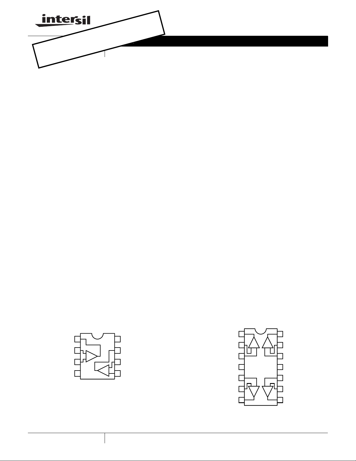
Pinouts
OUT
IN1-
IN1+
1
2
3
4
V-
EL2244
(8-PIN SO, PDIP)
TOP VIEW
-
+
-
+
1
EL2444
[14-PIN SO (0.150”), PDIP]
TOP VIEW
1
8
V+
7
OUT2
IN2-
6
IN2+
5
CAUTION: These devices are sensitive to electrostatic discharge; follow proper IC Handling Procedures.
1-888-INTERSIL or 1-888-352-6832
OUT1
IN1-
2
-+ -+
3
IN1+
V+
4
IN2+
5
-+ -+
6
IN2-
7
OUT2
| Intersil (and design) is a registered trademark of Intersil Americas Inc.
Copyright Intersil Americas Inc. 2004, 2005. All Rights Reserved
All other trademarks mentioned are the property of their respective owners.
14
OUT4
IN4-
13
12
IN4+
V-
11
IN3+
10
9
IN3-
OUT3
8
Page 2
Ordering Information
EL2244, EL2444
TAPE &
PART NUMBER PACKAGE
EL2244CM 16-Pin SO (0.300”) - MDP0027
EL2244CM-T13 16-Pin SO (0.300”) 13” MDP0027
EL2244CMZ
(See Note)
EL2244CMZ-T13
(See Note)
EL2244CN 8-Pin PDIP - MDP0031
EL2244CS 8-Pin SO - MDP0027
EL2244CS-T7 8-Pin SO 7” MDP0027
EL2244CS-T13 8-Pin SO 13” MDP0027
EL2244CSZ
(See Note)
EL2244CSZ-T7
(See Note)
EL2244CSZ-T13
(See Note)
EL2444CN 14-Pin PDIP - MDP0031
EL2444CS 14-Pin SO (0.150") - MDP0027
EL2444CS-T7 14-Pin SO (0.150") 7” MDP0027
EL2444CS-T13 14-Pin SO (0.150") 13” MDP0027
EL2444CSZ
(See Note)
EL2444CSZ-T7
(See Note)
EL2444CSZ-T13
(See Note)
NOTE: Intersil Pb-free products employ special Pb-free material sets;
molding compounds/die attach materials and 100% matte tin plate
termination finish, which are RoHS compliant and compatible with
both SnPb and Pb-free soldering operations. Intersil Pb-free products
are MSL classified at Pb-free peak reflow temperatures that meet or
exceed the Pb-free requirements of IPC/JEDEC J STD-020.
16-Pin SO (0.300”)
(Pb-free)
16-Pin SO (0.300”)
(Pb-free)
8-Pin SO
(Pb-free)
8-Pin SO
(Pb-free)
8-Pin SO
(Pb-free)
14-Pin SO (0.150")
(Pb-free)
14-Pin SO (0.150")
(Pb-free)
14-Pin SO (0.150")
(Pb-free)
REEL
- MDP0027
13” MDP0027
- MDP0027
7” MDP0027
13” MDP0027
- MDP0027
7” MDP0027
13” MDP0027
PKG.
DWG. #
2
Page 3
EL2244, EL2444
Absolute Maximum Ratings (T
Supply Voltage (V
Input Voltage (V
Differential Input Voltage (dVIN) . . . . . . . . . . . . . . . . . . . . . . . .±10V
Continuous Output Current . . . . . . . . . . . . . . . . . . . . . . . . . . . 40mA
CAUTION: Stresses above those listed in “Absolute Maximum Ratings” may cause permanent damage to the device. This is a stress only rating and operation of the
device at these or any other conditions above those indicated in the operational sections of this specification is not implied .
IMPORTANT NOTE: All parameters having Min/Max specifications are guaranteed. Typical values are for information purposes only. Unless otherwise noted, all tests
are at the specified temperature and are pulsed tests, therefore: T
). . . . . . . . . . . . . . . . . . . . . . . . . . . .±18V or 36V
S
. . . . . . . . . . . . . . . . . . . . . . . . . . . . . . . . . . . ±V
IN)
DC Electrical Specifications V
= 25°C)
A
Power Dissipation (P
S
Operating Temperature Range (T
Operating Junction Temperature (T
Storage Temperature (T
= TC = T
J
= ±15V, RL = 1kΩ, unless otherwise specified.
S
A
) . . . . . . . . . . . . . . . . . . . . . . . . . See Curves
D
ST
) . . . . . . . . . . . . .-40°C to +85°C
A
) . . . . . . . . . . . . . . . . . . +150°C
J
). . . . . . . . . . . . . . . . . . .-65°C to +150°C
PARAMETER DESCRIPTION CONDITION TEMP MIN TYP MAX UNIT
V
OS
TCV
I
B
I
OS
OS
Input Offset Voltage VS = ±15V 25°C 0.5 4.0 mV
T
Average Offset Voltage
, T
MIN
MAX
(Note 1) All 10.0 µV/°C
9.0 mV
Drift
Input Bias Current VS = ±15V 25°C 2.8 8.2 µA
T
, T
MIN
MAX
V
= ±5V 25°C 2.8 µA
S
11.2 µA
Input Offset Current VS = ±15V 25°C 50 300 nA
T
MIN
, T
MAX
500 nA
VS = ±5V 25°C 50 nA
TCI
OS
Average Offset Current
(Note 1) All 0.3 nA/°C
Drift
A
VOL
PSRR Power Supply Rejection
CMRR Common-mode
CMIR Common-mode Input
V
OUT
I
SC
Open-Loop Gain VS = ±15V, V
V
= ±5V, V
S
VS = ±5V, V
V
= ±5V to ±15V 25°C 65 80 dB
S
Ratio
= ±12V, V
V
Rejection Ratio
Range
CM
V
= ±15V 25°C ±14.0 V
S
VS = ±5V 25°C ±4.2 V
V
= +5V 25°C 4.2/0.1 V
S
= ±10V, RL = 1kΩ 25°C 800 1500 V/V
OUT
T
, T
MIN
MAX
= ±2.5V, RL = 500Ω 25°C 1200 V/V
OUT
= ±2.5V, RL = 150Ω 25°C 1000 V/V
OUT
T
, T
MIN
MAX
= 0V 25°C 70 90 dB
OUT
T
, T
MIN
MAX
600 V/V
60 dB
70 dB
Output Voltage Swing VS = ±15V, RL = 1kΩ 25°C ±13.4 ±13.6 V
Output Short Circuit
Current
, T
T
MIN
MAX
V
= ±15V, RL = 500Ω 25°C ±12.0 ±13.4 V
S
V
= ±5V, RL = 500Ω 25°C ±3.4 ±3.8 V
S
= ±5V, RL = 150Ω 25°C ±3.2 V
V
S
V
= +5V, RL = 500Ω 25°C 3.6/0.4 3.8/0.3 V
S
T
, T
MIN
MAX
25°C 40 75 mA
T
, T
MIN
MAX
±13.1 V
3.5/0.5 V
35 mA
3
Page 4
EL2244, EL2444
DC Electrical Specifications V
= ±15V, RL = 1kΩ, unless otherwise specified. (Continued)
S
PARAMETER DESCRIPTION CONDITION TEMP MIN TYP MAX UNIT
I
S
R
IN
Supply Current
(per amplifier)
VS = ±15V, no load 25°C 5.2 7 mA
T
MIN
T
MAX
= ±5V, no load 25°C 5.0 mA
V
S
7.6 mA
7.6 mA
Input Resistance Differential 25°C 150 kΩ
Common-mode 25°C 15 MΩ
C
IN
R
OUT
PSOR Power-Supply Operating
Input Capacitance AV = +1 @10MHz 25°C 1.0 pF
Output Resistance AV = +1 25°C 50 mΩ
Dual-supply 25°C ±2.0 ±18.0 V
Range
Single-supply 25°C 2.5 36.0 V
NOTE:
1. Measured from T
Closed-Loop AC Electrical Specifications V
MIN
to T
MAX
.
= ±15V, AV = +1, RL = 1kΩ, unless otherwise specified.
S
PARAMETER DESCRIPTION CONDITION TEMP MIN TYP MAX UNIT
BW -3dB Bandwidth
(V
= 0.4VPP)
OUT
GBWP Gain-Bandwidth Product V
PM Phase Margin R
= ±15V, AV = +1 25°C 120 MHz
V
S
= ±15V, AV = -1 25°C 60 MHz
V
S
= ±15V, AV = +2 25°C 60 MHz
V
S
= ±15V, AV = +5 25°C 12 MHz
V
S
= ±15V, AV = +10 25°C 6 MHz
V
S
= ±5V, AV = +1 25°C 80 MHz
V
S
= ±15V 25°C 60 MHz
S
= ±5V 25°C 45 MHz
V
S
= 1kΩ, CL = 10pF 25°C 50 °
L
CS Channel Separation f = 5MHz 25°C 85 dB
SR Slew Rate (Note 1) V
FPBW Full-Power Bandwidth
(Note 2)
, t
t
R
F
Rise Time, Fall Time 0.1V step 25°C 3.0 ns
= ±15V, RL = 1kΩ 25°C 250 325 V/µs
S
= ±5V, RL = 500Ω 25°C 200 V/µs
V
S
= ±15V 25°C 4.0 5.2 MHz
V
S
= ±5V 25°C 12.7 MHz
V
S
OS Overshoot 0.1V step 25°C 20 %
t
PD
t
S
Propagation Delay 25°C 2.5 ns
Settling to +0.1% (AV = +1) VS = ±15V, 10V step 25°C 80 ns
V
= ±5V, 5V step 25°C 60 ns
S
dG Differential Gain (Note 3) NTSC/PAL 25°C 0.04 %
dP Differential Phase (Note 3) NTSC/PAL 25°C 0.15 °
eN Input Noise Voltage 10kHz 25°C 15.0 nV/√Hz
iN Input Noise Current 10kHz 25°C 1.50 pA/√Hz
NOTES:
1. Slew rate is measured on rising edge
2. For V
= ±15V, V
S
(2π * Vpeak).
3. Video performance measured at V
= 20VPP. For VS = ±5V, V
OUT
= ±15V, AV = +2 with 2 times normal video level across RL = 150Ω. This corresponds to standard video
S
= 5VPP. Full-power bandwidth is based on slew rate measurement using: FPBW = SR /
OUT
levels across a back-terminated 75Ω load. For other values of R
4
, see curves.
L
Page 5

Typical Performance Curves
EL2244, EL2444
Non-Inverting
Frequency Response
Open-Loop Gain and
Phase vs Frequency
CMRR, PSRR and Closed-Loop
Output Resistance vs Frequency
Inverting Frequency Response
Output Voltage Swing
vs Frequency
2nd and 3rd Harmonic
Distortion vs Frequency
Frequency Response for
Various Load Resistances
Equivalent Input Noise
Settling Time vs
Output Voltage Change
Supply Current vs
Supply Voltage
5
Common-Mode Input Range
vs Supply Voltage
Output Voltage Range
vs Supply Voltage
Page 6

Typical Performance Curves (Continued)
EL2244, EL2444
Gain-Bandwidth Product
vs Supply Voltage
Bias and Offset Current
vs Input Common-Mode Voltage
Offset Voltage
vs Temperature
Open-Loop Gain
vs Supply Voltage
Open-Loop Gain
vs Load Resistance
Bias and Offset
Current vs Temperature
Slew-Rate vs
Supply Voltage
Voltage Swing
vs Load Resistance
Supply Current
vs Temperature
Gain-Bandwidth Product
vs Temperature
Short-Circuit Current
vs Temperature
Open-Loop Gain, PSRR
and CMRR vs Temperature
Small-Signal
Step Response
Slew Rate vs
Temperature
Large-Signal
Step Response
6
Page 7

Typical Performance Curves (Continued)
EL2244, EL2444
Differential Gain and
Phase vs DC Input
Offset at 3.58MHz
Differential Gain and
Phase vs Number of
150Ω Loads at 4.43MHz
Differential Gain and
Phase vs DC Input
Offset at 4.43MHz
Channel Separation
vs Frequency
Differential Gain and
Phase vs Number of
150Ω Loads at 3.58MHz
Overshoot vs Load Capacitance
60
VS=±15V
RG=Open
50
40
30
20
Overshoot (%)
10
0
510 30 5015 3525 4520 40
Load Capacitance (pF)
Package Power Dissipation vs Ambient Temperature
JEDEC JESD51-7 High Effective Thermal Conductivity Test
Board
2
1.786W
1.8
1.6
1.471W
1.4
1.420W
1.2
1.136W
1
0.8
0.6
Power Dissipation (W)
0.4
0.2
0
0 255075100 150
PDIP14
θJA=70°C/W
θJA=85°C/W
SO14
=88°C/W
θ
JA
85
Ambient Temperature (°C)
PDIP8
SO8
θJA=110°C/W
125
Gain-Bandwidth Product vs Load Capacitance
60
50
40
30
20
10
VS=±15V
Gain-Bandwidth Product (MHz)
AV=-2
0
110 10k100 1k
Load Capacitance (pF)
Package Power Dissipation vs Ambient Temperature
JEDEC JESD51-3 Low Effective Thermal Conductivity Test
Board
1.8
1.54W
1.6
1.4
1.25W
1.2
1
1.042W
0.8
781mW
0.6
Power Dissipation (W)
0.4
0.2
0
0 255075100 150
PDIP14
θ
=81°C/W
JA
SO8
θJA=160°C/W
85
Ambient Temperature (°C)
PDIP8
θ
=100°C/W
JA
SO14
θJA=120°C/W
125
7
Page 8

EL2244, EL2444
Simplified Schematic (Per Amplifier)
Burn-In Circuit (Per Amplifier)
calculate the maximum junction temperature (T
JMAX
) for all
applications to determine if power supply voltages, load
conditions, or package type need to be modified for the
EL2244 and EL2444 to remain in the safe operating area.
These parameters are related as follows:
T
JMAXTMAXΘJAPDMAXTOTAL
×()+=
where:
PD
MAXTOTAL
of each amplifier in the package (PD
is the sum of the maximum power dissipation
MAX
). PD
MAX
for each
amplifier can be calculated as follows:
V
PD
MAX
2VSI
SMAXVS
( - V
OUTMAX
)
OUTMAX
----------------------------×+××=
R
L
where:
T
= Maximum ambient temperature
MAX
θJA = Thermal resistance of the package
PD
= Maximum power dissipation of each amplifier
MAX
VS = Supply voltage
I
= Maximum supply current of each amplifier
SMAX
V
OUTMAX
= Maximum output voltage swing of the
application
ALL PACKAGES USE THE SAME SCHEMATIC
Applications Information
Product Description
The EL2244 and EL2444 are low-power wideband
monolithic operational amplifiers built on Elantec's
proprietary high-speed complementary bipolar process. The
EL2244 and EL2444 use a classical voltage-feedback
topology which allows them to be used in a variety of
applications where current-feedback amplifiers are not
appropriate because of restrictions placed upon the
feedback element used with the amplifier. The conventional
topology of the EL2244 and EL2444 allows, for example, a
capacitor to be placed in the feedback path, making it an
excellent choice for applications such as active filters,
sample-and-holds, or integrators. Similarly, because of the
ability to use diodes in the feedback network, the EL2244
and EL2444 are an excellent choice for applications such as
fast log amplifiers.
Power Dissipation
With the wide power supply range and large output drive
capability of the EL2244 and EL2444, it is possible to exceed
the 150°C maximum junction temperatures under certain
load and power-supply conditions. It is therefore important to
R
= Load resistance
L
To serve as a guide for the user, we can calculate maximum
allowable supply voltages for the example of the video
cable-driver below since we know that T
T
= 85°C, I
MAX
package θ
s are shown in Table 1. If we assume (for this
JA
= 7.6mA per amplifier, and the
SMAX
JMAX
= 150°C,
example) that we are driving a back-terminated video cable,
then the maximum average value (over duty-cycle) of
V
OUTMAX
is 1.4V, and RL = 150Ω, giving the results seen in
Table 1.
TABLE 1.
MAX PDISS
PART PACKAGE Θ
DUALS
EL2244CN PDIP8 100°C/W 0.650W @85°C ±16.6V
EL2244CS SO8 160°C/W 0.406W @85°C ±10.5V
QUADS
EL2444CN PDIP14 81°C/W 0.802W @85°C ±11.5V
EL2444CS SO14 120°C/W 0.542W @85°C ±7.5V
JA
@T
MAX
MAX V
Single-Supply Operation
The EL2244 and EL2444 have been designed to have a
wide input and output voltage range. This design also makes
the EL2244 and EL2444 an excellent choice for singlesupply operation. Using a single positive supply, the lower
S
8
Page 9

EL2244, EL2444
input voltage range is within 100mV of ground (RL = 500Ω),
and the lower output voltage range is within 300mV of
ground. Upper input voltage range reaches 4.2V, and output
voltage range reaches 3.8V with a 5V supply and R
This results in a 3.5V output swing on a single 5V supply.
This wide output voltage range also allows single-supply
operation with a supply voltage as high as 36V or as low as
2.5V. On a single 2.5V supply, the EL2244 and EL2444 still
have 1V of output swing.
= 500Ω.
L
Gain-Bandwidth Product and the -3dB Bandwidth
The EL2244 and EL2444 have a gain-bandwidth product of
120MHz while using only 5.2mA of supply current per
amplifier. For gains greater than 4, their closed-loop -3dB
bandwidth is approximately equal to the gain-bandwidth
product divided by the noise gain of the circuit. For gains
less than 4, higher-order poles in the amplifiers' transfer
function contribute to even higher closed loop bandwidths.
For example, the EL2244 and EL2444 have a -3dB
bandwidth of 120MHz at a gain of +1, dropping to 60MHz at
a gain of +2. It is important to note that the EL2244 and
EL2444 have been designed so that this “extra” bandwidth in
low-gain applications does not come at the expense of
stability. As seen in the typical performance curves, the
EL2244 and EL2444 in a gain of +1 only exhibit 1.0dB of
peaking with a 1kΩ load.
Video Performance
An industry-standard method of measuring the video
distortion of components such as the EL2244 and EL2444 is
to measure the amount of differential gain (dG) and
differential phase (dP) that they introduce. To make these
measurements, a 0.286V
device with 0V DC offset (0 IRE) at either 3.58MHz for NTSC
or 4.43MHz for PAL. A second measurement is then made
at 0.714V DC offset (100 IRE). Differential gain is a measure
of the change in amplitude of the sine wave, and is
measured in percent. Differential phase is a measure of the
change in phase, and is measured in degrees.
For signal transmission and distribution, a back-terminated
cable (75Ω in series at the drive end, and 75Ω to ground at
the receiving end) is preferred since the impedance match at
both ends will absorb any reflections. However, when double
termination is used, the received signal is halved; therefore a
gain of 2 configuration is typically used to compensate for
the attenuation.
The EL2244 and EL2444 have been designed as an
economical solution for applications requiring low video
distortion. They have been thoroughly characterized for
video performance in the topology described above, and the
results have been included as typical dG and dP
specifications and as typical performance curves. In a gain
of +2, driving 150Ω, with standard video test levels at the
input, the EL2244 and EL2444 exhibit dG and dP of only
0.04% and 0.15° at NTSC and PAL. Because dG and dP
(40 IRE) signal is applied to the
PP
can vary with different DC offsets, the video performance of
the EL2244 and EL2444 has been characterized over the
entire DC offset range from -0.714V to +0.714V. For more
information, refer to the curves of dG and dP vs DC Input
Offset.
Output Drive Capability
The EL2244 and EL2444 have been designed to drive low
impedance loads. They can easily drive 6V
load. This high output drive capability makes the EL2244
and EL2444 an ideal choice for RF, IF and video
applications. Furthermore, the current drive of the EL2244
and EL2444 remains a minimum of 35mA at low
temperatures.
into a 150Ω
PP
Printed-Circuit Layout
The EL2244 and EL2444 are well behaved, and easy to
apply in most applications. However, a few simple
techniques will help assure rapid, high quality results. As
with any high-frequency device, good PCB layout is
necessary for optimum performance. Ground-plane
construction is highly recommended, as is good power
supply bypassing. A 0.1µF ceramic capacitor is
recommended for bypassing both supplies. Lead lengths
should be as short as possible, and bypass capacitors
should be as close to the device pins as possible. For good
AC performance, parasitic capacitances should be kept to a
minimum at both inputs and at the output. Resistor values
should be kept under 5kΩ because of the RC time constants
associated with the parasitic capacitance. Metal-film and
carbon resistors are both acceptable, use of wire-wound
resistors is not recommended because of their parasitic
inductance. Similarly, capacitors should be low-inductance
for best performance.
The EL2244 and EL2444 Macromodel
This macromodel has been developed to assist the user in
simulating the EL2244 and EL2444 with surrounding
circuitry. It has been developed for the PSPICE simulator
(copywritten by the Microsim Corporation), and may need to
be rearranged for other simulators. It approximates DC, AC,
and transient response for resistive loads, but does not
accurately model capacitive loading. This model is slightly
more complicated than the models used for low-frequency
op-amps, but it is much more accurate for AC analysis.
The model does not simulate these characteristics
accurately:
•Noise
•Settling time
• Non-linearities
• Temperature effects
• Manufacturing variations
•CMRR
• PSRR
9
Page 10

EL2244 and EL244C Macromodel
* Connections: +input
* | -input
* | | +Vsupply
* | | | -Vsupply
* | | | | output
* | | | | |
.subckt M2244 3 2 7 4 6
*
* Input stage
*
ie 7 37 1mA
r6 36 37 800
r7 38 37 800
rc1 4 30 850
rc2 4 39 850
q1 30 3 36 qp
q2 39 2 38 qpa
ediff 33 0 39 30 1.0
rdiff 33 0 1Meg
*
* Compensation Section
*
ga 0 34 33 0 1m
rh 34 0 2Meg
ch 34 0 1.3pF
rc 34 40 1K
cc 40 0 1pF
*
* Poles
*
ep 41 0 40 0 1
rpa 41 42 200
cpa 42 0 1pF
rpb 42 43 200
cpb 43 0 1pF
*
* Output Stage
*
ios1 7 50 1.0mA
ios2 51 4 1.0mA
q3 4 43 50 qp
q4 7 43 51 qn
q5 7 50 52 qn
q6 4 51 53 qp
ros1 52 6 25
ros2 6 53 25
*
* Power Supply Current
*
ips 7 4 2.7mA
*
* Models
*
.model qn npn(is=800E-18 bf=200 tf=0.2nS)
.model qpa pnp(is=864E-18 bf=100 tf=0.2nS)
.model qp pnp(is=800E-18 bf=125 tf=0.2nS)
.ends
EL2244, EL2444
10
Page 11

EL2244, EL2444
EL2244 and EL2444 Macromodel (Continued)
All Intersil U.S. products are manufactured, assembled and tested utilizing ISO9000 quality systems.
Intersil Corporation’s quality certifications can be viewed at www.intersil.com/design/quality
Intersil products are sold by description only. Intersil Corporation reserves the right to make changes in circuit design, software and/or specifications at any time without
notice. Accordingly, the reader is cautioned to verify that data she ets are current before placin g orders. Information furn ished by Intersil is believed to be accurate and
reliable. However, no responsibility is assumed by Intersil or its subsidiaries for its use; nor for any infringements of patents or other rights of third parties which may result
from its use. No license is granted by implication or othe rwise under any patent or patent righ ts of Intersil or its subsidiaries.
For information regarding Intersil Corporation and its products, see www.intersil.com
11
Page 12

WWW.ALLDATASHEET.COM
Copyright © Each Manufacturing Company.
All Datasheets cannot be modified without permission.
This datasheet has been download from :
www.AllDataSheet.com
100% Free DataSheet Search Site.
Free Download.
No Register.
Fast Search System.
www.AllDataSheet.com
 Loading...