

Datasheet EL2228CY-T7, EL2228CY-T13, EL2228CY, EL2228CS-T7, EL2228CS-T13 Datasheet (ELANT)
...Page 1
EL2228C - Preliminary
Dual Low Noise Amplifier
EL2228C - Preliminary
Features
• Voltage noise of only 4.9nV/√Hz
• Current noise of only 1.2pA/√Hz
• Bandwidth (-3dB) of 80MHz -
@AV = +1
• Gain-of-1 stable
• Just 4.5mA per amplifier
• 8-pin MSOP package
• ±2.5V to ±12V operation
Applications
• ADSL Filters
• HDSLII Filters
• Ultrasound input amplifiers
• Wideband Instrumentation
• Communications equipment
• Wideband sensors
Ordering Information
Part No. Temp. Range Package Outline #
EL2228CY 8-Pin MSOP - MDP0043
EL2228CY-T13 8-Pin MSOP 13” MDP0043
EL2228CY-T7 8-Pin MSOP 7” MDP0043
EL2228CS 8-Pin SO - MDP0027
EL2228CS-T13 8-Pin SO 13” MDP0027
EL2228CS-T7 8-Pin SO 7” MDP0027
General Description
The EL2228C is a dual, low-noise amplifier, ideally suited to filtering
applications in ADSL and HDSLII designs. It feature low noise speci-
fication of just 4.9nV/√Hz and 1.2pA/√Hz, making it ideal for
processing low voltage waveforms.
The EL2228C has a -3dB bandwidth of 80MHz and is gain-of-1 stable. It also affords minimal power dissipation with a supply current of
just 4.5mA per amplifier. The amplifier can be powered from supplies
ranging from ±2.5V to ±12V.
The EL2228C is available in a space saving 8-Pin MSOP package as
well as the industry standard 8-Pin SO. It can operate over the -40°C to
+85°C temperature range.
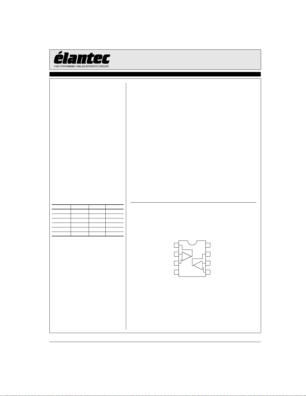
Connection Diagram
1
VOUTA
2
VINA-
VINA+
Note: All information contained in this data sheet has been carefully checked and is believed to be accurate as of the date of publication; however, this data sheet cannot be a “controlled document”. Current revisions, if any, to these
specifications are maintained at the factory and are available upon your request. We recommend checking the revision level before finalization of your design documentation.
© 2001 Elantec Semiconductor, Inc.
+
3
4
VS-
EL2228C
8-Pin SO and 8-Pin MSOP
8
VS+
7
VOUTB
65-
VINB-
+
VINB+
September 25, 2001
Page 2
EL2228C - Preliminary
Dual Low Noise Amplifier
Absolute Maximum Ratings (T
Values beyond absolute maximum ratings can cause the device to be prematurely damaged. Absolute maximum ratings are stress ratings only
and functional device operation is not implied.
Supply Voltage between VS+ and VS- +28V
EL2228C - Preliminary
Input Voltage VS- - 0.3V, VS +0.3V
Maximum Continuous Output Current 40mA
= 25°C)
A
Maximum Die Temperature +125°C
Storage Temperature -65°C to +150°C
Operating Temperature -40°C to +85°C
Lead Temperature 260°C
Power Dissipation See Curves
ESD Voltage 2kV
Important Note:
All parameters having Min/Max specifications are guaranteed. Typ values are for information purposes only. Unless otherwise noted, all tests are at the
specified temperature and are pulsed tests, therefore: TJ = TC = T
A
Electrical Characteristics
VS+= +12V, VS - = -12V, R
Parameter Description Condition Min Typ Max Unit
Input Characteristics
V
OS
TCV
I
B
R
IN
C
IN
Input Offset Voltage V
Average Offset Voltage Drift
OS
Input Bias Current V
Input Impedance 8 MΩ
Input Capacitance 1 pF
CMIR Common-Mode Input Range -11.8 +10.4 V
CMRR Common-Mode Rejection Ratio for VIN from -11.8V to +10.4V 60 90 dB
A
VOL
e
n
i
n
Open-Loop Gain -5V ≤ V
Voltage Noise f = 100kHz 4.9 nV/√Hz
Current Noise f = 100kHz 1.2 pA/√Hz
Output Characteristics
V
OL
V
OH
I
SC
Output Swing Low R
Output Swing High R
Short Circuit Current R
Power Supply Performance
PSRR Power Supply Rejection Ratio VS is moved from ±10.8V to ±13.2V 65 83 dB
I
S
Supply Current (Per Amplifier) No load 4 5 6 mA
Dynamic Performance
SR Slew Rate
t
S
Settling to +0.1% (AV = +1) (AV = +1), VO = 2V step 50 ns
BW -3dB Bandwidth 80 MHz
HD2 2nd Harmonic Distortion f = 1MHz, VO = 2V
HD3 3rd Harmonic Distortion f = 1MHz, VO = 2V
1. Measured over operating temperature range
2. Slew rate is measured on rising and falling edges
= 500Ω and C
L
[2]
= 3pF to 0V, R
L
= 420Ω & T
F
= 0V 0.2 3 mV
CM
[1]
= 0V -9 -4.5 -1 µA
CM
= 25°C unless otherwise specified.
A
-4 µV/°C
for VIN from -10V to +10V 60 75 dB
≤ 5V 60 75 dB
OUT
= 500Ω -10.3 -10 V
L
R
= 250Ω -9.5 -9 V
L
= 500Ω 10 10.3 V
L
R
= 250Ω 9.5 10 V
L
= 10Ω 140 180 mA
L
±2.5V square wave, measured 25%-75% 44 65 V/µs
, R
f = 1MHz, VO = 2V
f = 1MHz, VO = 2V
P-P
P-P
P-P
P-P
L
, R
L
, R
L
, R
L
= 500Ω, A
= 150Ω, A
= 500Ω, A
= 150Ω, A
= 2 -86 dBc
V
= 2 -79 dBc
V
= 2 -93 dBc
V
= 2 -70 dBc
V
2
Page 3
EL2228C - Preliminary
Dual Low Noise Amplifier
Electrical Characteristics
VS+= +5V, VS - = -5V, R
Parameter Description Condition Min Typ Max Unit
Input Characteristics
V
OS
TCV
OS
I
B
R
IN
C
IN
CMIR Common-Mode Input Range -4.7 +3.4 V
CMRR Common-Mode Rejection Ratio for VIN from -4.7V to +3.4V 60 90 dB
A
VOL
e
n
i
n
Output Characteristics
V
OL
V
OH
I
SC
Power Supply Performance
PSRR Power Supply Rejection Ratio VS is moved from ±4.5V to ±5.5V 65 83 dB
I
S
Dynamic Performance
SR Slew Rate
t
S
BW -3dB Bandwidth 75 MHz
HD2 2nd Harmonic Distortion f = 1MHz, VO = 2V
HD3 3rd Harmonic Distortion f = 1MHz, VO = 2V
1. Measured over operating temperature range
2. Slew rate is measured on rising and falling edges
= 500Ω and C
L
Input Offset Voltage V
Average Offset Voltage Drift
Input Bias Current V
= 3pF to 0V, R
L
= 420Ω & T
F
CM
[1]
CM
= 25°C unless otherwise specified.
A
= 0V 0.6 3 mV
4.9 µV/°C
= 0V -9 -4.5 -1 µA
Input Impedance 6 MΩ
Input Capacitance 1.2 pF
for VIN from -2V to +2V dB
Open-Loop Gain -2.5V ≤ V
≤ 2.5V 60 72 dB
OUT
Voltage Noise f = 100kHz 4.7 nV/√Hz
Current Noise f = 100kHz 1.2 pA/√Hz
Output Swing Low R
Output Swing High R
Short Circuit Current R
= 500Ω -3.8 -3.5 V
L
R
= 250Ω -3.7 -3.5 V
L
= 500Ω 3.5 3.7 V
L
R
= 250Ω 3.5 3.6 V
L
= 10Ω 60 100 mA
L
Supply Current (Per Amplifier) No load 3.5 4.5 5.5 mA
[2]
±2.5V square wave, measured 25%-75% 35 50 V/µs
Settling to +0.1% (AV = +1) (AV = +1), VO = 2V step 50 ns
, R
f = 1MHz, VO = 2V
f = 1MHz, VO = 2V
P-P
P-P
P-P
P-P
= 500Ω, A
L
, R
= 150Ω, A
L
, R
= 500Ω, A
L
, R
= 150Ω, A
L
= 2 -90 dBc
V
= 2 -71 dBc
V
= 2 -99 dBc
V
= 2 -69 dBc
V
EL2228C - Preliminary
3
Page 4
EL2228C - Preliminary
Dual Low Noise Amplifier
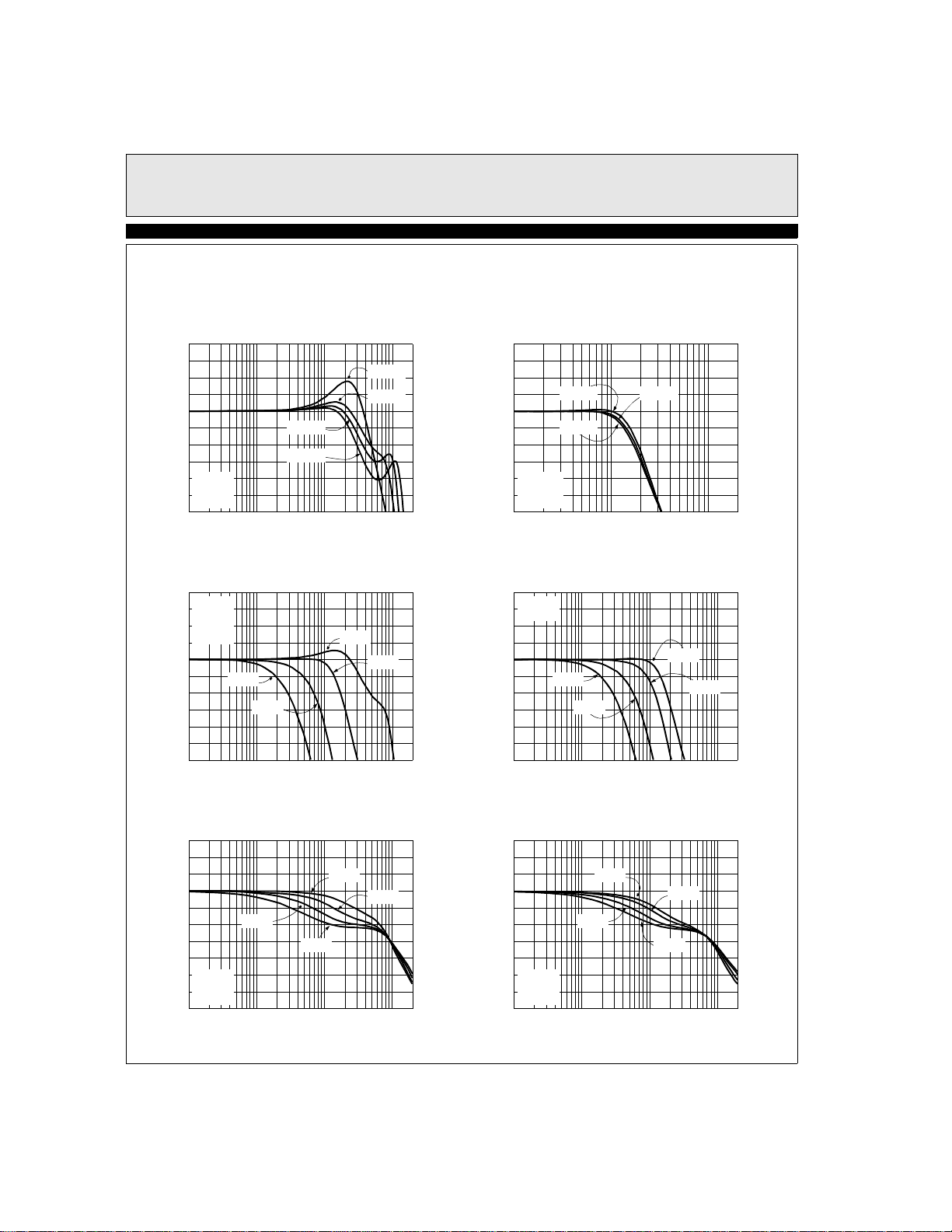
Typical Performance Curves
Non-inverting Frequency Response for Various R
EL2228C - Preliminary
4
3
2
1
0
-1
-2
-3
Normalized Gain (dB)
-4
VS=±12V
AV=+1
-5
RL=500Ω
-6
100k 1M
Non-inverting Frequency Response (Gain)
4
VS=±12V
3
RF=420Ω
RL=500Ω
2
AV=+1
1
0
-1
-2
-3
Normalized Gain (dB)
-4
-5
-6
100k 1M 10M
AV=10
RF=200Ω
RF=0Ω
Frequency (Hz)
AV=5
Frequency (Hz)
10M
AV=1
F
RF=1kΩ
RF=420Ω
100M
AV=2
100M
Inverting Frequency Response for Various R
4
3
2
1
0
-1
-2
-3
Normalized Gain (dB)
-4
-5
-6
1M 10M
Inverting Frequency Response (Gain)
4
3
2
1
0
-1
-2
-3
Normalized Gain (dB)
-4
-5
-6
100k 1M 10M
RF=100Ω RF=420Ω
RF=1kΩ
VS=±12V
AV=-1
RL=500Ω
VS=±12V
RF=420Ω
AV=-10
AV=-5
Frequency (Hz)
Frequency (Hz)
F
100M
AV=-1
AV=-2
100M
Non-inverting Frequency Response (Phase)
135
90
45
0
-45
-90
Phase (°)
-135
-180
-225
VS=±12V
RF=420Ω
-270
RL=500Ω
-315
100k 1M 10M
AV=5
AV=10
Frequency (Hz)
AV=1
AV=2
100M
Inverting Frequency Response (Phase)
135
90
45
0
-45
-90
Phase (°)
-135
-180
-225
VS=±12V
RF=420Ω
-270
RL=500Ω
-315
100k
AV=-1
AV=-2
AV=-5
AV=-10
10M1M 100M
Frequency (Hz)
4
Page 5

Typical Performance Curves
EL2228C - Preliminary
EL2228C - Preliminary
Dual Low Noise Amplifier
Non-inverting Frequency Response for Various
Input Signal Levels
4
VS=±12V
3
RF=420Ω
RL=500Ω
2
AV=+1
1
0
-1
-2
-3
Normalized Gain (dB)
-4
-5
-6
100k 1M
Non-inverting Frequency Response for Various C
4
3
2
1
0
-1
-2
-3
Normalized Gain (dB)
VS=±12V
RF=420Ω
-4
RL=500Ω
-5
AV=+1
-6
100k 1M 10M
VIN=1V
PP
VIN=2V
PP
VIN=500mV
Frequency (Hz)
CL=3pF
Frequency (Hz)
PP
10M
CL=30pF
CL=10pF
VIN=100mV
100M
100M
Non-inverting Frequency Response for Various R
4
3
2
1
PP
L
0
-1
-2
-3
Normalized Gain (dB)
-4
VS=±12V
AV=+1
-5
RF=420Ω
-6
100k 1M
Non-inverting Frequency Response for Various
Output DC Levels
4
3
2
1
0
-1
-2
-3
Normalized Gain (dB)
VS=±12V
RF=420Ω
-4
RL=500Ω
-5
AV=+1
-6
100k 1M 10M
RL=50Ω
RL=150Ω
RL=500Ω
10M
Frequency (Hz)
VO=-10
VO=+5
VO=-5
Frequency (Hz)
VO=+10
L
RL=1kΩ
100M
VO=0
100M
-3dB Bandwidth vs ±Supply Voltage for Noninverting Gains
80
G=1
60
40
-3dB Bandwidth (MHz)
20
0
2.5 4.5 8.5
G=2
G=5 G=10
6.5 10.5
Supply Voltage (±V)
VS=±12V
RF=420Ω
RL=500Ω
AV=+1
12.5
-3dB Bandwidth vs ±Supply Voltage for Inverting
Gains
25
VS=±12V
20
RF=420Ω
RL=500Ω
AV=+1
15
10
-3dB Bandwidth (MHz)
5
0
2.5
Supply Voltage (±V)
G=-1
G=-2
G=-5
G=-10
8.54.5 12.5
10.56.5
5
Page 6

EL2228C - Preliminary
Dual Low Noise Amplifier
Typical Performance Curves
Peaking vs ±Supply Voltage for Non-inverting
EL2228C - Preliminary
Gains
1
0.8
0.6
0.4
Peaking (dB)
0.2
G=10
0
2.5 4.5
Small Signal Step Response
VS=±12V
20mV/div
G=1
G=2
8.56.5 10.5
Supply Voltage (±V)
VS=±12V
RF=420Ω
RL=500Ω
AV=+1
RF=420Ω
AV=1
RL=500Ω
12.5
Peaking vs ±Supply Voltage for Inverting Gains
0.2
0.16
0.12
0.08
Peaking (dB)
0.04
0
2.5 8.54.5 10.56.5 12.5
Small Signal Step Response
VS=±2.5V
20mV/div
G=-1
Supply Voltage (±V)
G=-10
RF=420Ω
AV=1
RL=500Ω
VS=±12V
RF=420Ω
RL=500Ω
AV=+1
G=-2
Large Signal Step Response
VS=±12V
0.5V/div
50ns/div
50ns/div
RF=420Ω
AV=1
RL=500Ω
50ns/div
Large Signal Step Response
VS=±2.5V
RF=420Ω
AV=1
RL=500Ω
0.5V/div
50ns/div
6
Page 7

Typical Performance Curves
EL2228C - Preliminary
EL2228C - Preliminary
Dual Low Noise Amplifier
Group Delay vs Frequency
20
16
12
8
4
0
-4
Group Delay (ns)
-8
-12
-16
-20
1M
Supply Current vs Supply Voltage
13.2
12
10.8
9.6
8.4
7.2
6
4.8
Supply Current (mA)
3.6
2.4
1.2
0
0
VS=±12V
RF=420Ω
AV=1
RL=500Ω
AV=2
AV=1
Frequency (Hz)
5.6 11.22.8 8.4 12.64.2 9.81.4 7
VS (±V)
Differential Gain/Phase vs DC Input Voltage at
3.58MHz
0.2
VS=±12V
RF=420Ω
0.15
RL=150Ω
AV=2
0.1
0.05
0
dG (%) or dP (°)
-0.05
-0.1
100M10M
200M
14
-0.15
-1 -0.5 0
DC Input Voltage (V)
Closed Loop Output Impedance vs Frequency
100
10
1
Output Impedance (Ω)
0.1
0.01
10k
dP
dG
10.5
100M1M 10M100k
Frequency (Hz)
CMRR
100
80
60
40
-CMRR (dB)
20
VS=±12
0
10
100k 100M1k 1M10k 10M100
Frequency (Hz)
-10
-30
-50
-70
-90
PSRR
10
VS-
VS+
100M10k 100k 1M 10M1k
Frequency (Hz)
7
Page 8

EL2228C - Preliminary
Dual Low Noise Amplifier
Typical Performance Curves
1MHz 2nd and 3rd Harmonic Distortion vs Output
EL2228C - Preliminary
Swing (VS=±12V)
-40
-50
-60
-70
Distortion (dB)
-80
-90
-100
0 8
Output Swing (VPP)
1MHz 2nd and 3rd Harmonic Distortion vs Output
Swing (single-ended)
-50
-60
-70
3rd HD
-80
-90
Distortion (dBc)
-100
-110
-120
2nd HD
Output Swing (VPP)
2ndH
3rdH
VS=±12V
AV=2
RF=420Ω
20124 16
204 8 12 160
1MHz 2nd and 3rd Harmonic Distortion vs Output
Swing (VS=±2.5V)
-50
-60
-70
-80
Distortion (dB)
-90
-100
-110
0 1 2.51.50.5 2
1MHz 2nd and 3rd Harmonic Distortion vs Output
Swing (single-ended)
-50
VS=±2.5V
AV=2
-60
RF=420Ω
-70
-80
Distortion (dBc)
-90
-100
-110
3rdH
Output Swing (VPP)
2nd D
UT
3rd D
Output Swing (VPP)
2ndH
UT
2.50.5 1 1.5 20
Voltage and Current Noise vs Frequency
18
16
14
12
10
8
6
4
2
Voltage Noise (nV√Hz), Current Noise
0
10 100 10k
E
N
I
N
Frequency (Hz)
Channel to Channel Isolation vs Frequency
0
-20
-40
Gain (dB)
-60
-80
1k
100k
-100
100k 1M 10M
Frequency (Hz)
A → B
B → C
100M
8
Page 9

Typical Performance Curves
EL2228C - Preliminary
EL2228C - Preliminary
Dual Low Noise Amplifier
IS vs Tempertaure
VS=±12V
11
10
S
I
9
0
IB vs Temperature
-2
-4
(µA)
B
I
-6
-8
50
Temperature (mA)
Temperature (°C)
3dB Bandwidth vs Temperature
VS=±5V
100
90
80
70
Bandwidth (MHz)
60
1500 100-50
1500 50 100-50
50
VOS vs Temperature
2
1
0
(mV)
OS
V
-1
-2
Junction Temperature (°C)
10.1
Temperature (°C)
16010 60 110-40
1010.1
SR vs Temperature
76
74
72
70
68
SR (V/µs)
66
64
62
Temperature (°C)
Package Power Dissipation vs Ambient Temp.
JEDEC JESD51-3 Low Effective Thermal Conductivity Test Board
0.7
0.6
625mW
0.5
486mW
0.4
0.3
0.2
Power Dissipation (W)
0.1
1500 50 100-50
0
MSOP8
206°C/W
SO8
160°C/W
10085
Ambient Temperature (°C)
15025 50 75 1250
9
Page 10

EL2228C - Preliminary
Dual Low Noise Amplifier
Pin Descriptions
EL2228C - Preliminary
EL2228CY
8-Pin MSOP
EL2228CS 8-
Pin SO Pin Name Pin Function Equivalent Circuit
10
Page 11

Applications Information
Product Description
EL2228C - Preliminary
EL2228C - Preliminary
Dual Low Noise Amplifier
11
Page 12

EL2228C - Preliminary
Dual Low Noise Amplifier
EL2228C - Preliminary
General Disclaimer
Specifications contained in this data sheet are in effect as of the publication date shown. Elantec, Inc. reserves the right to make changes in the circuitry or specifications contained herein at any time without notice. Elantec, Inc. assumes no responsibility for the use of any circuits described
herein and makes no representations that they are free from patent infringement.
WARNING - Life Support Policy
Elantec, Inc. products are not authorized for and should not be used
within Life Support Systems without the specific written consent of
Elantec, Inc. Life Support systems are equipment intended to sup-
Elantec Semiconductor, Inc.
675 Trade Zone Blvd.
Milpitas, CA 95035
Telephone: (408) 945-1323
(888) ELANTEC
Fax: (408) 945-9305
European Office: +44-118-977-6020
Japan Technical Center: +81-45-682-5820
port or sustain life and whose failure to perform when properly used
in accordance with instructions provided can be reasonably
expected to result in significant personal injury or death. Users contemplating application of Elantec, Inc. Products in Life Support
Systems are requested to contact Elantec, Inc. factory headquarters
to establish suitable terms & conditions for these applications. Elantec, Inc.’s warranty is limited to replacement of defective
components and does not cover injury to persons or property or
other consequential damages.
September 25, 2001
12
Printed in U.S.A.
 Loading...