

Datasheet EDS5116ABTA-7A, EDS5116ABTA-75, EDS5116ABTA-6B, EDS5108ABTA-7A, EDS5108ABTA-75 Datasheet (ELPID)
...Page 1
PRELIMINARY DATA SHEET
512M bits SDRAM
EDS5104ABTA (128M words ×××× 4 bits)
EDS5108ABTA (64M words ×××× 8 bits)
EDS5116ABTA (32M words ×××× 16 bits)
Description
The EDS5104AB is a 512M bits SDRAM organized as
33,554,432 words × 4 bits × 4 banks. The EDS5108AB
is a 512M bits SDRAM organized as 16,777,216 words
× 8 bits × 4 banks. The EDS5116AB is a 512M bits
SDRAM organized as 8,388,608 words × 16 bits × 4
banks. All inputs and outputs are referred to the rising
edge of the clock input. It is packaged in standard 54pin plastic TSOP (II).
Features
• 3.3V power supply
• Clock frequency: 166MHz/133MHz (max.)
• LVTTL interface
• Single pulsed /RAS
• 4 banks can operate simultaneously and
independently
• Burst read/write operation and burst read/single write
operation capability
• Programmable burst length (BL): 1, 2, 4, 8, full page
• 2 variations of burst sequence
Sequential (BL = 1, 2, 4, 8, full page)
Interleave (BL = 1, 2, 4, 8)
• Programmable /CAS latency (CL): 2, 3
• Byte control by DQM
: DQM (EDS5104AB, EDS5108AB)
: UDQM, LDQM (EDS5116AB)
• Refresh cycles: 8192 refresh cycles/64ms
• 2 variations of refresh
Auto refresh
Self refresh
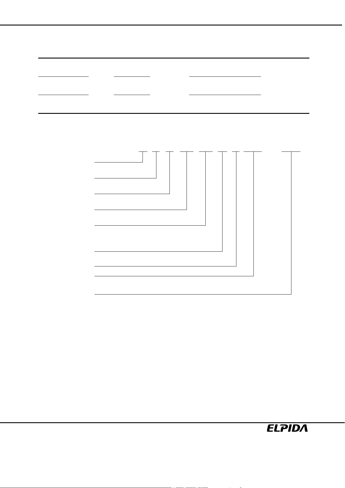
Pin Configurations
/xxx indicates active low signal.
54-pin Plastic TSOP (II)
VDD
NC
VDDQ
NC
DQ0
VSSQ
NC
NC
VDDQ
NC
DQ1
VSSQ
NC
VDD
NC
/WE
/CAS
/RAS
/CS
BA0
BA1
A10
A0
A1
A2
A3
VDD
A0 to A12,
BA0, BA1
DQ0 to DQ15
/CS
/RAS
/CAS
/WE
VDD
VDD
DQ0
VDDQ
NC
DQ1
VSSQ
NC
DQ2
VDDQ
NC
DQ3
VSSQ
NC
VDD
LDQM
NC
/WE
/CAS
/RAS
/CS
BA0
BA1
A10
A0
A1
A2
A3
VDD
Address input
Bank select address
Data-input/output
Chip select
Row address strobe
Column address strobe
Write enable
DQ0
VDDQ
DQ1
DQ2
VSSQ
DQ3
DQ4
VDDQ
DQ5
DQ6
VSSQ
DQ7
VDD
/WE
/CAS
/RAS
/CS
BA0
BA1
A10
A0
A1
A2
A3
VDD
1
2
3
4
5
6
7
8
9
10
11
12
13
14
15
16
17
18
19
20
21
22
23
24
25
26
27
(Top view)
X 16
X 8
X 4
DQM
CKE
CLK
VDD
VSS
VDDQ
VSSQ
NC
54
53
52
51
50
49
48
47
46
45
44
43
42
41
40
39
38
37
36
35
34
33
32
31
30
29
28
DQ7
DQ15
VSSQ
VSSQ
DQ14
NC
DQ13
DQ6
VDDQ
VDDQ
DQ12
NC
DQ11
DQ5
VSSQ
VSSQ
DQ10
NC
DQ9
DQ4
VDDQ
VDDQ
DQ8
NC
VSS
VSS
NC
NC
UDQM
DQM
CLK
CLK
CKE
CKE
A12
A12
A11
A11
A9
A9
A8
A8
A7
A7
A6
A6
A5
A5
A4
A4
VSS
VSS
Input/output mask
Clock enable
Clock input
Power for internal circuit
Ground for internal circuit
Power for DQ circuit
Ground for DQ circuit
No connection
VSS
VSS
VSS
NC
VSSQ
NC
DQ3
VDDQ
NC
NC
VSSQ
NC
DQ2
VDDQ
NC
VSS
NC
DQM
CLK
CKE
A12
A11
A9
A8
A7
A6
A5
A4
VSS
Document No. E0250E20 (Ver. 2.0)
Date Published October 2002 (K) Japan
URL: http://www.elpida.com
Elpida Memory, Inc. 2002
Page 2
EDS5104ABTA, EDS5108ABTA, EDS5116ABTA
Ordering Information
Part number
EDS5104ABTA-6B
EDS5104ABTA-7A
EDS5104ABTA-75*
EDS5108ABTA-6B
EDS5108ABTA-7A
EDS5108ABTA-75*
EDS5116ABTA-6B
EDS5116ABTA-7A
EDS5116ABTA-75*
Note: 100MHz operation at /CAS latency = 2.
Mask
Version
B 128M × 4 4
64M × 8
32M × 16
Organization
(words × bits)
Part Number
E D S 51 04 A B TA - 6B
Elpida Memory
Type
D: Monolithic Device
Internal Banks
Clock frequency
MHz (max.)
166
133
133
166
133
133
166
133
133
/CAS latency Package
3
2, 3
3
3
2, 3
3
3
2, 3
3
54-pin Plastic
TSOP (II)
Product Code
S: SDRAM
Density / Bank
51: 512M/4-Bank
Bit Organization
04: x4
08: x8
16: x16
Voltage,Interface
A: 3.3V, LVTTL
Die Rev.
Package
TA: TSOP (II)
Speed
6B: 166MHz/CL3
7A: 133MHz/CL2, 3
75: 133MHz/CL3
100MHz/CL2
Preliminary Data Sheet E0250E20 (Ver. 2.0)
2
Page 3

CONTENTS
EDS5104ABTA, EDS5108ABTA, EDS5116ABTA
Description.....................................................................................................................................................1
Features.........................................................................................................................................................1
Pin Configurations .........................................................................................................................................1
Ordering Information......................................................................................................................................2
Part Number ..................................................................................................................................................2
Electrical Specifications.................................................................................................................................4
Block Diagram .............................................................................................................................................12
Pin Function.................................................................................................................................................13
Command Operation ...................................................................................................................................15
Simplified State Diagram .............................................................................................................................23
Mode Register Configuration.......................................................................................................................24
Power-up Sequence ....................................................................................................................................26
Operation of the SDRAM .............................................................................................................................27
Timing Waveforms.......................................................................................................................................43
Package Drawing ........................................................................................................................................49
Recommended Soldering Conditions ..........................................................................................................50
Preliminary Data Sheet E0250E20 (Ver. 2.0)
3
Page 4
EDS5104ABTA, EDS5108ABTA, EDS5116ABTA
Electrical Specifications
• All voltages are referenced to VSS (GND).
• After power up (refer to the Power-up Sequence).
Absolute Maximum Ratings
Parameter Symbol Rating Unit Note
Voltage on any pin relative to VSS VT –0.5 to VDD + 0.5 (≤ 4.6 (max.)) V
Supply voltage relative to VSS VDD –0.5 to +4.6 V
Short circuit output current IOS 50 mA
Power dissipation PD 1.0 W
Operating temperature TA 0 to +70 °C
Storage temperature Tstg –55 to +125 °C
Caution
Exposing the device to stress above those listed in Absolute Maximum Ratings could cause
permanent damage. The device is not meant to be operated under conditions outside the limits
described in the operational section of this specification. Exposure to Absolute Maximum Rating
conditions for extended periods may affect device reliability.
Recommended Operating Conditions (TA = 0 to 70°°°°C)
Parameter Symbol min. max. Unit Notes
Supply voltage VDD, VDDQ 3.0 3.6 V 1
VSS, VSSQ 0 0 V 2
Input high voltage VIH 2.0 VDD + 0.3 V 3
Input low voltage VIL –0.3 0.8 V 4
Notes: 1. The supply voltage with all VDD and VDDQ pins must be on the same level.
2. The supply voltage with all VSS and VSSQ pins must be on the same level.
3. VIH (max.) = VDD + 2.0 V for pulse width ≤ 3ns at VDD.
4. VIL (min.) = VSS – 2.0 V for pulse width ≤ 3ns at VSS.
Preliminary Data Sheet E0250E20 (Ver. 2.0)
4
Page 5
EDS5104ABTA, EDS5108ABTA, EDS5116ABTA
DC Characteristics 1 (TA = 0 to +70°°°°C, VDD, VDDQ = 3.3V ± 0.3V, VSS, VSSQ = 0V)
Parameter max.
/CAS latency Symbol Grade × 4 × 8 × 16 Unit Test condition Notes
Operating current ICC1
Standby current in power
down
Standby current in power
down (input signal stable)
Standby current in non
power down
Standby current in non
power down (input signal
stable)
Active standby current in
power down
Active standby current in
power down (input signal
stable)
Active standby current in
non power down
Active standby current in
non power down (input
signal stable)
Burst operating current ICC4
Refresh current ICC5
Self refresh current ICC6 4 4 4 mA
ICC2P 3 3 3 mA
ICC2PS 2 2 2 mA CKE = VIL, tCK = ∞ 7
ICC2N
ICC2NS 9 9 9 mA
ICC3P 4 4 4 mA
ICC3PS 3 3 3 mA CKE = VIL, tCK = ∞ 2, 7
ICC3N
ICC3NS 20 20 20 mA
-6B,-7A
-75
-6B
-7A, -75
-6B
-7A, -75
-6B
-7A, -75
-6B,-7A
-75
Notes: 1. ICC depends on output load condition when the device is selected. ICC (max.) is specified at the output
open condition.
2. One bank operation.
3. Input signals are changed once per one clock.
4. Input signals are changed once per two clocks.
5. Input signals are changed once per four clocks.
6. After power down mode, CLK operating current.
7. After power down mode, no CLK operating current.
8. Input signals are VIH or VIL fixed.
160
140
30
25
45
40
160
130
320
280
165
145
30
25
45
40
170
140
320
280
175
155
30
25
45
40
190
160
320
280
mA
mA
mA
mA tCK = tCK (min.), BL = 4 1, 2, 5
mA tRC = tRC (min.) 3
Burst length = 1
tRC = tRC (min.)
CKE = VIL,
tCK = tCK (min.)
CKE, /CS = VIH,
tCK = tCK (min.)
CKE = VIH, tCK = ∞,
/CS = VIH
CKE = VIL,
tCK = tCK (min.)
CKE, /CS = VIH,
tCK = tCK (min.)
CKE = VIH, tCK = ∞,
/CS = VIH
VIH ≥ VDD – 0.2V
VIL ≤ 0.2V
1, 2, 3
6
4
8
1, 2, 6
1, 2, 4
2, 8
DC Characteristics 2 (TA = 0 to +70°°°°C, VDD, VDDQ = 3.3V ± 0.3V, VSS, VSSQ = 0V)
Parameter Symbol min. max. Unit Test condition Notes
Input leakage current ILI –1 1 µA 0 ≤ VIN ≤ VDD
Output leakage current ILO –1.5 1.5 µA 0 ≤ VOUT ≤ VDD, DQ = disable
Output high voltage VOH 2.4 — V IOH = –4 mA
Output low voltage VOL — 0.4 V IOL = 4 mA
Preliminary Data Sheet E0250E20 (Ver. 2.0)
5
Page 6
EDS5104ABTA, EDS5108ABTA, EDS5116ABTA
Pin Capacitance (TA = 25°C, VDD, VDDQ = 3.3V ± 0.3V)
Parameter Symbol Pins min. Typ max. Unit
Input capacitance CI1 CLK 2.5 — 3.5 pF
CI2
Data input/output capacitance CI/O DQ 4 — 6.5 pF
Address, CKE, /CS, /RAS,
/CAS, /WE, DQM,
2.5 — 3.8 pF
Notes: 1. Capacitance measured with Boonton Meter or effective capacitance measuring method.
2. Measurement condition: f = 1MHz, 1.4V bias, 200mV swing.
3. DQM = VIH to disable DOUT.
4. This parameter is sampled and not 100% tested.
AC Characteristics (TA = 0 to +70°°°°C, VDD, VDDQ = 3.3V ± 0.3V, VSS, VSSQ = 0V)
-6B -7A -75
Parameter Symbol min. max. min. max. min. max. Unit Notes
System clock cycle time tCK 6.0 — 7.5 — 7.5 — ns 1
CLK high pulse width tCH 2.5 — 2.5 — 2.5 — ns 1
CLK low pulse width tCL 2.5 — 2.5 — 2.5 — ns 1
Access time from CLK tAC — 5.0 — 5.4 — 5.4 ns 1, 2
Data-out hold time tOH 2.5 — 3.0 — 3.0 — ns 1, 2
CLK to Data-out low impedance tLZ 1 — 1 — 1 — ns 1, 2, 3
CLK to Data-out high impedance tHZ — 5.4 — 5.4 — 5.4 ns 1, 4
Input setup time tSI 1.5 — 1.5 — 1.5 — ns 1
Input hold time tHI 0.8 — 0.8 — 0.8 — ns 1
Ref/Active to Ref/Active command
period
Active to Precharge command
period
Active command to column
command (same bank)
Precharge to active command
period
Write recovery or data-in to
precharge lead time
Last data into active latency tDAL
Active (a) to Active (b) command
period
Transition time (rise and fall) tT 0.5 5 0.5 5 0.5 5 ns
Refresh period
(8192 refresh cycles)
tRC 60 — 60 — 67.5 — ns 1
tRAS 42 120000 45 120000 45 120000 ns 1
tRCD 18 — 15 — 20 — ns 1
tRP 18 — 15 — 20 — ns 1
tDPL 12 — 15 — 15 — ns 1
2CLK +
18ns
tRRD 12 — 15 — 15 — ns 1
tREF — 64 — 64 — 64 ms
—
2CLK +
15ns
—
2CLK +
20ns
—
Notes: 1. AC measurement assumes tT = 0.5ns. Reference level for timing of input signals is 1.4V.
2. Access time is measured at 1.4V. Load condition is CL = 50pF.
3. tLZ (min.) defines the time at which the outputs achieves the low impedance state.
4. tHZ (max.) defines the time at which the outputs achieves the high impedance state.
Notes
1, 2, 4
1, 2, 4
1, 2, 3, 4
Preliminary Data Sheet E0250E20 (Ver. 2.0)
6
Page 7
EDS5104ABTA, EDS5108ABTA, EDS5116ABTA
Test Conditions
• Input and output timing reference levels: 1.4V
• Input waveform and output load: See following figures
2.4 V
0.4 V
2.0 V
0.8 V
t
T
tT
input
Output load
Relationship Between Frequency and Minimum Latency
Parameter -6B -7A -75
Frequency (MHz) 166 133
tCK (ns) Symbol 6.0 7.5 7.5 Notes
Active command to column command
(same bank)
Active command to active command
(same bank)
Active command to precharge command
(same bank)
Precharge command to active command
(same bank)
Write recovery or data-in to precharge
command (same bank)
Active command to active command
(different bank)
Self refresh exit time lSREX 1 1 1 2
Last data in to active command
(Auto precharge, same bank)
Self refresh exit to command input lSEC 10 8 9
Precharge command to high impedance
(CL = 2)
(CL = 3) lHZP 3 3 3
Last data out to active command
(Auto precharge, same bank)
Last data out to precharge (early precharge)
(CL = 2)
(CL = 3) lEP –2 –2 –2
Column command to column command lCCD 1 1 1
Write command to data in latency lW CD 0 0 0
DQM to data in lDID 0 0 0
DQM to data out lDOD 2 2 2
CKE to CLK disable lCLE 1 1 1
Register set to active command lMRD 2 2 2
/CS to command disable lCDD 0 0 0
Power down exit to command input lPEC 1 1 1
lRCD 3 2 3 1
lRC 10 8 9 1
lRAS 7 6 6 1
lRP 3 2 3 1
lDPL 2 2 2 1
lRRD 2 2 2 1
lDAL 5 4 5 = [lDPL + lRP]
lHZP
lAPR 1 1 1
lEP
—
—
2
–1
Notes: 1. IRCD to IRRD are recommended value.
2. Be valid [DESL] or [NOP] at next command of self refresh exit.
3. Except [DESL] and [NOP]
I/O
2
–1
CL
= [lRC]
3
Preliminary Data Sheet E0250E20 (Ver. 2.0)
7
Page 8
EDS5104ABTA, EDS5108ABTA, EDS5116ABTA
VIL/VIH Clamp
This SDRAM component has VIL and VIH clamp for CLK, CKE, /CS, DQM and DQ pins.
[Minimum VIL Clamp Current]
VIL (V) I (mA)
–2 –32
–1.8 –25
–1.6 –19
–1.4 –13
–1.2 –8
–1 –4
–0.9 –2
–0.8 –0.6
–0.6 0
–0.4 0
–0.2 0
0 0
–5
–10
–15
–20
I (mA)
–25
–30
–35
0
–2
–1.5 –1 –0.5
VIL (V)
0
Minimum VIL Clamp Current
Preliminary Data Sheet E0250E20 (Ver. 2.0)
8
Page 9
EDS5104ABTA, EDS5108ABTA, EDS5116ABTA
[Minimum VIH Clamp Current]
VIH (V) I (mA)
VDD + 2 10
VDD + 1.8 8
VDD + 1.6 5.5
VDD + 1.4 3.5
VDD + 1.2 1.5
VDD + 1 0.3
VDD + 0.8 0
VDD + 0.6 0
VDD + 0.4 0
VDD + 0.2 0
VDD + 0 0
10
8
6
I (mA)
4
2
0
VDD + 0 VDD + 1 VDD + 2VDD + 0.5 VDD + 1.5
VIH (V)
Minimum VIH Clamp Current
Preliminary Data Sheet E0250E20 (Ver. 2.0)
9
Page 10
EDS5104ABTA, EDS5108ABTA, EDS5116ABTA
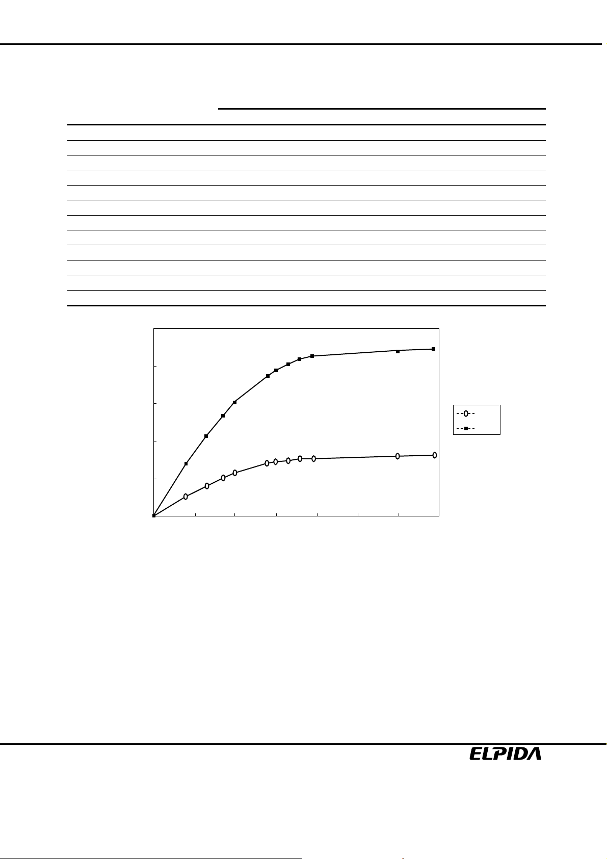
IOL/IOH Characteristics
[Output Low Current (IOL)]
IOL IOL
VOUT (V) min. (mA) max. (mA)
0 0 0
0.4
0.65
0.85
1
1.4
1.5
1.65
1.8
1.95
3
3.45
250
27.5 70.2
41.8 107.5
51.6 133.8
58.0 151.2
70.7 187.7
72.9 194.4
75.4 202.5
77.0 208.6
77.6 212.0
80.3 219.6
81.4 222.6
200
150
IOL (mA)
100
50
0
0 0.5 1 1.5 2 2.5 3 3.5
VOUT (V)
Output Low Current (IOL)
min.
max.
Preliminary Data Sheet E0250E20 (Ver. 2.0)
10
Page 11
EDS5104ABTA, EDS5108ABTA, EDS5116ABTA
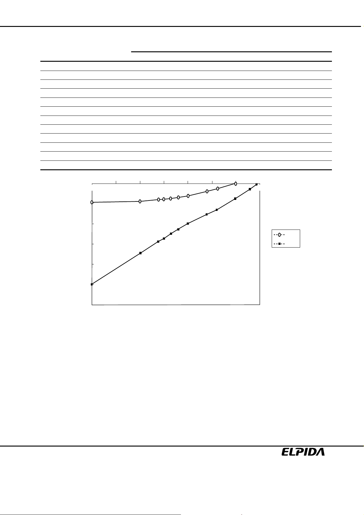
[Output High Current (IOH)]
IOH IOH
VOUT (V) min. (mA) max. (mA)
3.45 —
3.3 —
3 0
2.6
2.4
2
1.8
1.65
1.5
1.4
1
0
−21.1 −129.2
−34.1 −153.3
−58.7 −197.0
−67.3 −226.2
−73.0 −248.0
−77.9 −269.7
−80.8 −284.3
−88.6 −344.5
−93.0 −502.4
0
0.5 1 1.5 2 2.5 3
−2.4
−27.3
−74.1
3.50
–100
–200
IOH (mA)
–300
–400
–500
–600
VOUT(V)
Output High Current (IOH)
min.
max.
Preliminary Data Sheet E0250E20 (Ver. 2.0)
11
Page 12
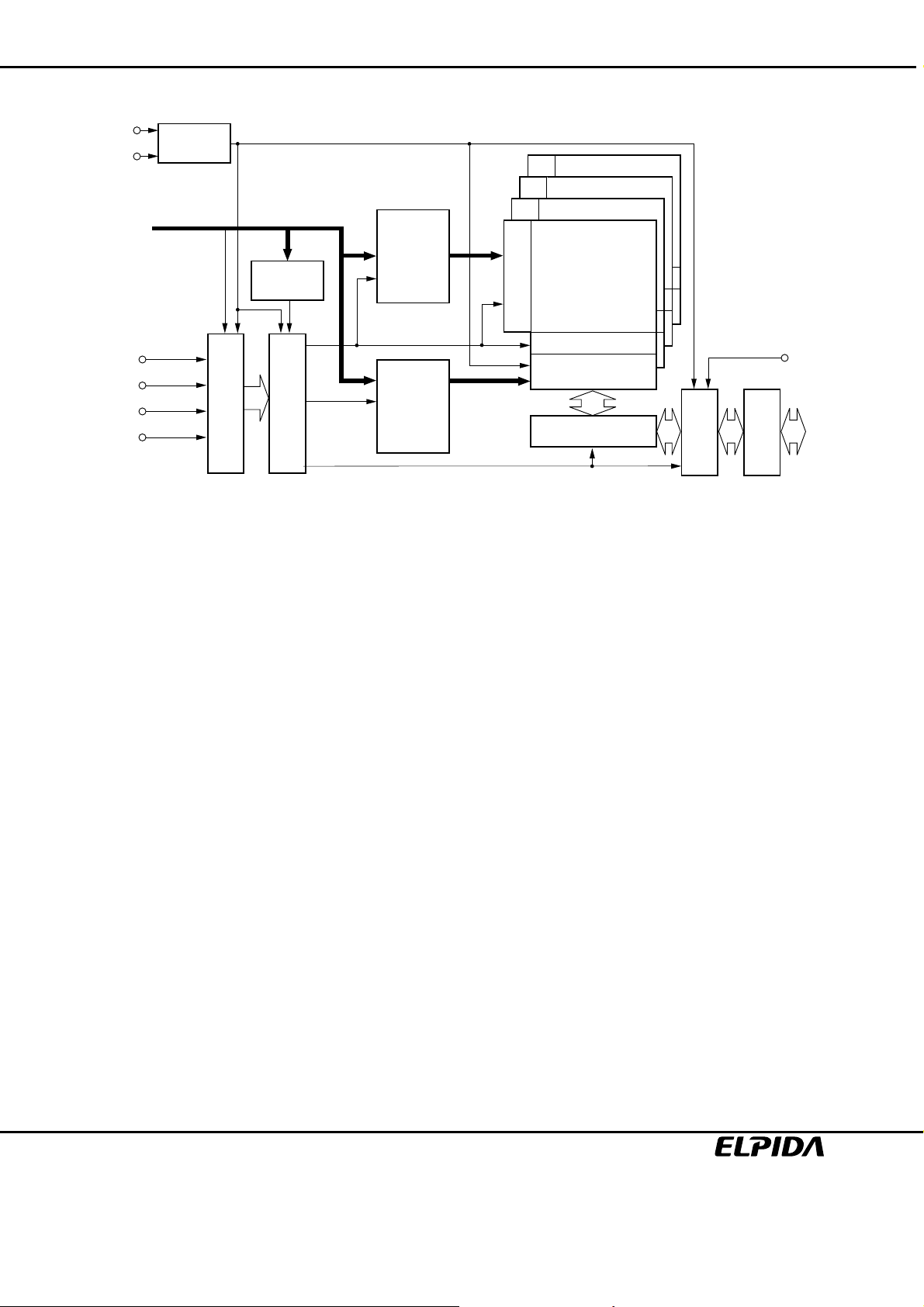
Block Diagram
CLK
CKE
Address
/CS
/RAS
/CAS
/WE
Clock
Generator
Mode
Register
Control Logic
Command Decoder
EDS5104ABTA, EDS5108ABTA, EDS5116ABTA
Bank 3
Bank 2
Row
Address
Buffer
&
Refresh
Counter
Row Decoder
Column
Address
Buffer
&
Burst
Counter
Bank 1
Bank 0
Sense Amplifier
Column Decoder &
Latch Circuit
Data Control Circuit
Latch Circuit
DQM
DQ
Input & Output
Buffer
Preliminary Data Sheet E0250E20 (Ver. 2.0)
12
Page 13
EDS5104ABTA, EDS5108ABTA, EDS5116ABTA
Pin Function
CLK (input pin)
CLK is the master clock input to this pin. The other input signals are referred at CLK rising edge.
/CS (input pin)
When /CS is Low, the command input cycle becomes valid. When /CS is High, all inputs are ignored. However,
internal operations (bank active, burst operations, etc.) are held.
/RAS, /CAS, and /WE (input pins)
Although these pin names are the same as those of conventional DRAMs, they function in a different way. These
pins define operation commands (read, write, etc.) depending on the combination of their voltage levels. For details,
refer to the command operation section.
A0 toA12 (input pins)
Row address (AX0 to AX12) is determined by A0 to A12 at the bank active command cycle CLK rising edge.
Column address is determined by A0 to A9, A11 or A12 (see Address Pins Table) at the read or write command
cycle CLK rising edge. And this column address becomes burst access start address.
[Address Pins Table]
Address (A0 to A12)
Part number Row address Column address
EDS5104AB AX0 to AX12 AY0 to AY9, AY11, AY12
EDS5108AB AX0 to AX12 AY0 to AY9, AY11
EDS5116AB AX0 to AX12 AY0 to AY9
A10 defines the precharge mode. When A10 = High at the precharge command cycle, all banks are precharged.
But when A10 = Low at the precharge command cycle, only the bank that is selected by BA0 and BA1 (BS) is
precharged. For details refer to the command operation section.
BA0 and BA1 (input pin)
BA0 and BA1 are bank select signal (BS). (See Bank Select Signal Table)
[Bank Select Signal Table]
BA0 BA1
Bank 0 L L
Bank 1 H L
Bank 2 L H
Bank 3 H H
Remark: H: VIH. L: VIL.
CKE (input pin)
This pin determines whether or not the next CLK is valid. If CKE is High, the next CLK rising edge is valid. If CKE is
Low, the next CLK rising edge is invalid. This pin is used for power-down mode, clock suspend mode and self
refresh mode.
Preliminary Data Sheet E0250E20 (Ver. 2.0)
13
Page 14

EDS5104ABTA, EDS5108ABTA, EDS5116ABTA
DQM, UDQM and LDQM (input pins)
DQM controls input/output buffers. In 32M × 16 products, UDQM and LDQM control upper byte (DQ8 to DQ15) and
lower byte (DQ0 to DQ7).
Read operation: If DQM is High, the output buffer becomes High-Z. If the DQM is Low, the output buffer becomes
Low-Z. (The latency of DQM during reading is 2 clocks.)
Write operation: If DQM is High, the previous data is held (the new data is not written). If DQM is Low, the data is
written. (The latency of DQM during writing is 0 clock.)
DQ0 toDQ15 (input/output pins)
Data is input to and output from these pins (DQ0 to DQ3; EDS5104AB , DQ0 to DQ7; EDS5108AB, DQ0 to DQ15;
EDS5116AB).
VDD, VSS, VDDQ, VSSQ (Power supply)
VDD and VSS are power supply pins for internal circuits. VDDQ and VSSQ are power supply pins for the output
buffers.
Preliminary Data Sheet E0250E20 (Ver. 2.0)
14
Page 15
EDS5104ABTA, EDS5108ABTA, EDS5116ABTA
Command Operation
Command Truth Table
The SDRAM recognizes the following commands specified by the /CS, /RAS, /CAS, /WE and address pins.
CKE
Function Symbol n – 1 n /CS /RAS /CAS /WE BA1,BA0 A10
Device deselect DESL H × H × × × × × ×
No operation NOP H × L H H H × × ×
Burst stop BST H × L H H L × × ×
Read READ H × L H L H V L V
Read with auto precharge READA H × L H L H V H V
Write WRIT H × L H L L V L V
Write with auto precharge WRITA H × L H L L V H V
Bank activate ACT H × L L H H V V V
Precharge select bank PRE H × L L H L V L ×
Precharge all banks PALL H × L L H L × H ×
Mode register set MRS H × L L L L L L V
Remark: H: VIH. L: VIL. ×: VIH or VIL. V: Valid address input.
Device deselect command [DESL]
When this command is set (/CS is High), the SDRAM ignore command input at the clock. However, the internal
status is held.
No operation [NOP]
This command is not an execution command. However, the internal operations continue.
Burst stop command [BST]
This command can stop the current burst operation.
Column address strobe and read command [READ]
This command starts a read operation. In addition, the start address of burst read is determined by the column
address (see Address Pins Table in Pin Function) and the bank select address (BA0, BA1). After the read operation,
the output buffer becomes High-Z.
Read with auto-precharge [READA]
This command automatically performs a precharge operation after a burst read with a burst length of 1, 2, 4 or 8.
Column address strobe and write command [WRIT]
This command starts a write operation. When the burst write mode is selected, the column address (see Address
Pins Table in Pin Function) and the bank select address (BA0, BA1) become the burst write start address. When the
single write mode is selected, data is only written to the location specified by the column address (see Address Pins
Table in Pin Function) and the bank select address (BA0, BA1).
Write with auto-precharge [WRITA]
This command automatically performs a precharge operation after a burst write with a length of 1, 2, 4 or 8, or after a
single write operation.
A0 to A12
Preliminary Data Sheet E0250E20 (Ver. 2.0)
15
Page 16
EDS5104ABTA, EDS5108ABTA, EDS5116ABTA
Row address strobe and bank activate [ACT]
This command activates the bank that is selected by BA0, BA1 and determines the row address (AX0 to AX12).
(See Bank Select Signal Table)
Precharge selected bank [PRE]
This command starts precharge operation for the bank selected by BA0, BA1. (See Bank Select Signal Table)
[Bank Select Signal Table]
BA0 BA1
Bank 0 L L
Bank 1 H L
Bank 2 L H
Bank 3 H H
Remark: H: VIH. L: VIL.
Precharge all banks [PALL]
This command starts a precharge operation for all banks.
Refresh [REF/SELF]
This command starts the refresh operation. There are two types of refresh operation, the one is auto-refresh, and
the other is self-refresh. For details, refer to the CKE truth table section.
Mode register set [MRS]
The SDRAM has a mode register that defines how it operates. The mode register is specified by the address pins
(A0 to A12, BA0 and BA1) at the mode register set cycle. For details, refer to the mode register configuration. After
power on, the contents of the mode register are undefined, execute the mode register set command to set up the
mode register.
Preliminary Data Sheet E0250E20 (Ver. 2.0)
16
Page 17

EDS5104ABTA, EDS5108ABTA, EDS5116ABTA
DQM Truth Table
CKE DQM
Commands Symbol n – 1 n UDQM LDQM
Write enable/output enable ENB H × L
Write inhibit/output disable MASK H × H
Upper byte write enable/output enable ENBU H × L ×
Lower byte write enable/output enable ENBL H × × L
Upper byte write inhibit/output disable MASKU H × H ×
Lower byte write inhibit/output disable MASKL H × × H
Remark: H: VIH. L: VIL. ×: VIH or VIL
Write: IDID is needed.
Read: IDOD is needed.
CKE Truth Table
CKE
Current state Function Symbol n – 1 n /CS /RAS /CAS /WE Address
Activating Clock suspend mode entry H L × × × × ×
Any Clock suspend mode L L × × × × ×
Clock suspend Clock suspend mode exit L H × × × × ×
Idle CBR (auto) refresh command REF H H L L L H ×
Idle Self refresh entry SELF H L L L L H ×
Self refresh Self refresh exit L H L H H H ×
L H H × × × ×
Idle Power down entry H L L H H H ×
H L H × × × ×
Power down Power down exit L H H × × × ×
L H L H H H ×
Remark: H: VIH. L: VIL. ×: VIH or VIL
Preliminary Data Sheet E0250E20 (Ver. 2.0)
17
Page 18

EDS5104ABTA, EDS5108ABTA, EDS5116ABTA
Function Truth Table
The following table shows the operations that are performed when each command is issued in each mode of the
SDRAM.
The following table assumes that CKE is high.
Current state /CS /RAS /CAS /WE Address Command Operation
Precharge H × × × × DESL Enter IDLE after tRP
L H H H × NOP Enter IDLE after tRP
L H H L × BST ILLEGAL
L H L H BA, CA, A10 READ/READA ILLEGAL*3
L H L L BA, CA, A10 WRIT/WRITA ILLEGAL*3
L L H H BA, RA ACT ILLEGAL*3
L L H L BA, A10 PRE, PALL NOP*5
L L L H × REF, SELF ILLEGAL
L L L L MODE MRS ILLEGAL
Idle H × × × × DESL NOP
L H H H × NOP NOP
L H H L × BST ILLEGAL
L H L H BA, CA, A10 READ/READA ILLEGAL*4
L H L L BA, CA, A10 WRIT/WRITA ILLEGAL*4
L L H H BA, RA ACT Bank and row active
L L H L BA, A10 PRE, PALL NOP
L L L H × REF, SELF Refresh
L L L L MODE MRS Mode register set*8
Row active H × × × × DESL NOP
L H H H × NOP NOP
L H H L × BST ILLEGAL
L H L H BA, CA, A10 READ/READA Begin read*6
L H L L BA, CA, A10 WRIT/WRITA Begin write*6
L L H H BA, RA ACT
L L H L BA, A10 PRE, PALL Precharge*7
L L L H × REF, SELF ILLEGAL
L L L L MODE MRS ILLEGAL
Read H × × × × DESL Continue burst to end
L H H H × NOP Continue burst to end
L H H L × BST Burst stop
L H L H BA, CA, A10 READ/READA
L H L L BA, CA, A10 WRIT/WRITA Term burst read/start write
L L H H BA, RA ACT
L L H L BA, A10 PRE, PALL Term burst read and Precharge
L L L H × REF, SELF ILLEGAL
L L L L MODE MRS ILLEGAL
Other bank active
ILLEGAL on same bank*
Continue burst read to /CAS
latency and New read
Other bank active
ILLEGAL on same bank*
2
2
Preliminary Data Sheet E0250E20 (Ver. 2.0)
18
Page 19

EDS5104ABTA, EDS5108ABTA, EDS5116ABTA
Current state /CS /RAS /CAS /WE Address Command Operation
Read with autoprecharge
L H H H × NOP
L H H L × BST ILLEGAL
L H L H BA, CA, A10 READ/READA ILLEGAL*3
L H L L BA, CA, A10 WRIT/WRITA ILLEGAL*3
L L H H BA, RA ACT
L L H L BA, A10 PRE, PALL ILLEGAL*3
L L L H × REF, SELF ILLEGAL
L L L L MODE MRS ILLEGAL
Write H × × × × DESL Continue burst to end
L H H H × NOP Continue burst to end
L H H L × BST Burst stop
L H L H BA, CA, A10 READ/READA Term burst and New read
L H L L BA, CA, A10 WRIT/WRITA Term burst and New write
L L H H BA, RA ACT
L L H L BA, A10 PRE, PALL Term burst write and Precharge*1
L L L H × REF, SELF ILLEGAL
L L L L MODE MRS ILLEGAL
Write with autoprecharge
L H H H × NOP
L H H L × BST ILLEGAL
L H L H BA, CA, A10 READ/READA ILLEGAL*3
L H L L BA, CA, A10 WRIT/WRITA ILLEGAL*3
L L H H BA, RA ACT
L L H L BA, A10 PRE, PALL ILLEGAL*3
L L L H × REF, SELF ILLEGAL
L L L L MODE MRS ILLEGAL
Refresh (auto-refresh) H × × × × DESL Enter IDLE after tRC
L H H H × NOP Enter IDLE after tRC
L H H L × BST ILLEGAL
L H L H BA, CA, A10 READ/READA ILLEGAL*4
L H L L BA, CA, A10 WRIT/WRITA ILLEGAL*4
L L H H BA, RA ACT ILLEGAL*4
L L H L BA, A10 PRE, PALL ILLEGAL*4
L L L H × REF, SELF ILLEGAL
L L L L MODE MRS ILLEGAL
H × × × × DESL
H × × × × DESL
Continue burst to end and
precharge
Continue burst to end and
precharge
Other bank active
ILLEGAL on same bank*
Other bank active
ILLEGAL on same bank*
Continue burst to end and
precharge
Continue burst to end and
precharge
Other bank active
ILLEGAL on same bank*
2
3
3
Preliminary Data Sheet E0250E20 (Ver. 2.0)
19
Page 20

EDS5104ABTA, EDS5108ABTA, EDS5116ABTA
Current state /CS /RAS /CAS /WE Address Command Operation
Mode register set H × × × × DESL NOP
L H H H × NOP NOP
L H H L × BST ILLEGAL
L H L H BA, CA, A10 READ/READA ILLEGAL*4
L H L L BA, CA, A10 WRIT/WRITA ILLEGAL*4
L L H H BA, RA ACT Bank and row active*9
L L H L BA, A10 PRE, PALL NOP
L L L H × REF, SELF Refresh*
L L L L MODE MRS Mode register set*8
Remark: H: VIH. L: VIL. ×: VIH or VIL
Notes: 1. An interval of tDPL is required between the final valid data input and the precharge command.
2. If tRRD is not satisfied, this operation is illegal.
3. Illegal for same bank, except for another bank.
4. Illegal for all banks.
5. NOP for same bank, except for another bank.
6. Illegal if tRCD is not satisfied.
7. Illegal if tRAS is not satisfied.
8. MRS command must be issued after DOUT finished, in case of DOUT remaining.
9. Illegal if lMRD is not satisfied.
9
Preliminary Data Sheet E0250E20 (Ver. 2.0)
20
Page 21

EDS5104ABTA, EDS5108ABTA, EDS5116ABTA
Command Truth Table for CKE
CKE
Current State n – 1 n /CS /RAS /CAS /WE Address Operation Notes
Self refresh H × × × × × × INVALID, CLK (n – 1) would exit self refresh
L H H × × × × Self refresh recovery
L H L H H × × Self refresh recovery
L H L H L × × ILLEGAL
L H L L × × × ILLEGAL
L L × × × × × Continue self refresh
Self refresh recovery H H H × × × × Idle after t
H H L H H × × Idle after t
H H L H L × × ILLEGAL
H H L L × × × ILLEGAL
H L H × × × × ILLEGAL
H L L H H × × ILLEGAL
H L L H L × × ILLEGAL
H L L L × × × ILLEGAL
Power down H × × × × × INVALID, CLK (n – 1) would exit power down
L H H × × × × EXIT power down
L H L H H H × EXIT power down
L L × × × × × Continue power down mode
All banks idle H H H × × × Refer to operations in Function Truth Table
H H L H × × Refer to operations in Function Truth Table
H H L L H × Refer to operations in Function Truth Table
H H L L L H × CBR (auto) Refresh
H H L L L L OPCODE Refer to operations in Function Truth Table
H L H × × × Begin power down next cycle
H L L H × × Refer to operations in Function Truth Table
H L L L H × Refer to operations in Function Truth Table
H L L L L H × Self refresh 1
H L L L L L OPCODE Refer to operations in Function Truth Table
L H × × × × × Exit power down next cycle
L L × × × × × Power down 1
Row active H × × × × × × Refer to operations in Function Truth Table
L × × × × × × Clock suspend 1
Any state other than H H × × × × Refer to operations in Function Truth Table
listed above H L × × × × × Begin clock suspend next cycle 2
L H × × × × × Exit clock suspend next cycle
L L × × × × × Maintain clock suspend
Remark: H: VIH. L: VIL. ×: VIH or VIL
Notes: 1. Self refresh can be entered only from the all banks idle state. Power down can be entered only from all
banks idle. Clock suspend can be entered only from following states, row active, read, read with autoprecharge, write and write with auto precharge.
2. Must be legal command as defined in Function Truth Table.
RC
RC
Preliminary Data Sheet E0250E20 (Ver. 2.0)
21
Page 22

EDS5104ABTA, EDS5108ABTA, EDS5116ABTA
Clock suspend mode entry
The SDRAM enters clock suspend mode from active mode by setting CKE to Low. If command is input in the clock
suspend mode entry cycle, the command is valid. The clock suspend mode changes depending on the current
status (1 clock before) as shown below.
ACTIVE clock suspend
This suspend mode ignores inputs after the next clock by internally maintaining the bank active status.
READ suspend and READ with Auto-precharge suspend
The data being output is held (and continues to be output).
WRITE suspend and WRIT with Auto-precharge suspend
In this mode, external signals are not accepted. However, the internal state is held.
Clock suspend
During clock suspend mode, keep the CKE to Low.
Clock suspend mode exit
The SDRAM exits from clock suspend mode by setting CKE to High during the clock suspend state.
IDLE
In this state, all banks are not selected, and completed precharge operation.
Auto-refresh command [REF]
When this command is input from the IDLE state, the SDRAM starts auto-refresh operation. (The auto-refresh is the
same as the CBR refresh of conventional DRAMs.) During the auto-refresh operation, refresh address and bank
select address are generated inside the SDRAM. For every auto-refresh cycle, the internal address counter is
updated. Accordingly, 8192 times are required to refresh the entire memory. Before executing the auto-refresh
command, all the banks must be in the IDLE state. In addition, since the precharge for all banks is automatically
performed after auto-refresh, no precharge command is required after auto-refresh.
Self-refresh entry [SELF]
When this command is input during the IDLE state, the SDRAM starts self-refresh operation. After the execution of
this command, self-refresh continues while CKE is Low. Since self-refresh is performed internally and automatically,
external refresh operations are unnecessary.
Power down mode entry
When this command is executed during the IDLE state, the SDRAM enters power down mode. In power down
mode, power consumption is suppressed by cutting off the initial input circuit.
Self-refresh exit
When this command is executed during self-refresh mode, the SDRAM can exit from self-refresh mode. After exiting
from self-refresh mode, the SDRAM enters the IDLE state.
Power down exit
When this command is executed at the power down mode, the SDRAM can exit from power down mode. After
exiting from power down mode, the SDRAM enters the IDLE state.
Preliminary Data Sheet E0250E20 (Ver. 2.0)
22
Page 23

Simplified State Diagram
EDS5104ABTA, EDS5108ABTA, EDS5116ABTA
SELF
REFRESH
SR ENTRY
SR EXIT
WRITE
SUSPEND
WRITEA
SUSPEND
MODE
REGISTER
SET
Write
CKE_
CKE
WRITE
WITH AP
CKE_
CKE
BST
MRS
ACTIVE
CLOCK
SUSPEND
CKE
WRITE
WRITE
WITH
AP
WRITE
READ
WITH AP
WRITEA
PRECHARGE PRECHARGE
IDLE
ACTIVE
CKE_
ROW
ACTIVE
READ
WRITE
PRECHARGE
CKE_
READ
WITH
AP
WRITE
WITH AP
REFRESH
CKE
READ
AUTO
REFRESH
IDLE
POWER
DOWN
BST
READ
READ
WITH AP
READA
*1
Read
CKE_
CKE
CKE_
CKE
READ
SUSPEND
READA
SUSPEND
POWER
APPLIED
POWER
ON
PRECHARGE
PRECHARGE
Automatic transition after completion of command.
Transition resulting from command input.
Note: 1. After the auto-refresh operation, precharge operation is performed automatically and
enter the IDLE state.
Preliminary Data Sheet E0250E20 (Ver. 2.0)
23
Page 24

EDS5104ABTA, EDS5108ABTA, EDS5116ABTA
Mode Register Configuration
The mode register is set by the input to the address pins (A0 to A12, BA0 and BA1) during mode register set cycles.
The mode register consists of five sections, each of which is assigned to address pins.
BA1, BA0, A8, A9, A10, A11, A12: (OPCODE): The SDRAM has two types of write modes. One is the burst write
mode, and the other is the single write mode. These bits specify write mode.
Burst read and burst write: Burst write is performed for the specified burst length starting from the column address
specified in the write cycle.
Burst read and single write: Data is only written to the column address specified during the write cycle, regardless of
the burst length.
A7: Keep this bit Low at the mode register set cycle. If this pin is high, the vender test mode is set.
A6, A5, A4: (LMODE): These pins specify the /CAS latency.
A3: (BT): A burst type is specified.
A2, A1, A0: (BL): These pins specify the burst length.
BA1
0
X
X
X
BA0BA1
BA0
0
X
X
X
A12
A12
0
X
X
X
A11
A10
A9 A8 A7 A6 A5 A4 A3 A2 A1 A0
OPCODE 0 LMODE BT BL
A3
A10
A11
00
X
X
X
X
X
X
000
001
010
011 3
1XX R
A9
0
0R
1 Burst read and single write
1R1
Write modeA8
Burst read and burst write
0
1
0
R
R
2
0 Sequential
1 Interleave
Burst typeA6 A5 A4 CAS latency
F.P.: Full Page
R is Reserved (inhibit)
X: 0 or 1
A2 A1 A0
000
001
010
011 8
100 R
101 R R
110 R
111
Mode Register Set Timing
Burst length
BT=0 BT=1
1
1
2
2
4
4
8
R
R
F.P.
R
Preliminary Data Sheet E0250E20 (Ver. 2.0)
24
Page 25

EDS5104ABTA, EDS5108ABTA, EDS5116ABTA
Burst length = 2
Starting Ad.
A0
0
1
Burst length = 8
Starting Ad.
A2 A1 A0
000
001
010
011
100
101
110
111
Addressing(decimal)
InterleaveSequential
0, 1,
1, 0,
Addressing(decimal)
0, 1, 2, 3, 4, 5, 6, 7,
1, 2, 3, 4, 5, 6, 7,
2, 3, 4, 5, 6, 7,
3, 4, 5, 6, 7,
4, 5, 6, 7,
5, 6, 7,
6, 7,
7,
0, 1,
1, 0,
0, 1, 2, 3,
0, 1, 2, 3, 4,
0, 1, 2, 3, 4, 5,
0, 1, 2, 3, 4, 5, 6,
Burst length = 4
Starting Ad.
A1 A0
00
01
10
11
InterleaveSequential
0, 1, 2, 3, 4, 5, 6, 7,
0,
1, 0, 3, 2, 5, 4, 7,
0, 1,
0, 1, 2,
Burst Sequence
2, 3, 0, 1, 6, 7,
3, 2, 1, 0, 7,
4, 5, 6, 7,
5, 4, 7,
6, 7,
7,
Addressing(decimal)
InterleaveSequential
0, 1, 2, 3,
1, 2, 3, 0,
2, 3, 0, 1,
3,
0, 1, 2,
0, 1, 2, 3,
6, 1, 0, 3, 2,
4, 5, 2, 3, 0, 1,
6, 5, 4, 3, 2, 1, 0,
0, 1, 2, 3,
1, 0, 3, 2,
2, 3, 0, 1,
3, 2, 1, 0,
4, 5,
6, 5, 4,
6,
Full page burst is available only for sequential addressing. The addressing sequence is started from the column
address that is asserted by read/write command. And the address is increased one by one.
It is back to the address 0 when the address reaches at the end of address 4,095 (for 128M ×4 device), 2,047 (for
64M × 8 device) and 1,023 (for 32M × 16 device). “Full page” never stops the burst read/write.
Preliminary Data Sheet E0250E20 (Ver. 2.0)
25
Page 26

EDS5104ABTA, EDS5108ABTA, EDS5116ABTA
Power-up Sequence
Power-up Sequence
The SDRAM should be goes on the following sequence with power up.
The CLK, CKE, /CS, DQM and DQ pins keep low till power stabilizes.
The CLK pin is stabilized within 100 µs after power stabilizes before the following initialization sequence.
The CKE and DQM is driven to high between power stabilizes and the initialization sequence.
This SDRAM has VDD clamp diodes for CLK, CKE, /CS DQM and DQ pins. If these pins go high before power up,
the large current flows from these pins to VDD through the diodes.
Initialization Sequence
When 200 µs or more has past after the above power-up sequence, all banks must be precharged using the
precharge command (PALL). After tRP delay, set 8 or more auto refresh commands (REF). Set the mode register
set command (MRS) to initialize the mode register. We recommend that by keeping DQM and CKE to High, the
output buffer becomes High-Z during Initialization sequence, to avoid DQ bus contention on memory system formed
with a number of device.
Power up sequence
Initialization sequence
VDD, VDDQ
CKE, DQM
CLK
/CS, DQ
100 µs
0 V
Low
Low
Low
Power stabilize
Power-up sequence and Initialization sequence
200 µs
Preliminary Data Sheet E0250E20 (Ver. 2.0)
26
Page 27

EDS5104ABTA, EDS5108ABTA, EDS5116ABTA
Operation of the SDRAM
Read/Write Operations
Bank active
Before executing a read or write operation, the corresponding bank and the row address must be activated by the
bank active (ACT) command. An interval of tRCD is required between the bank active command input and the
following read/write command input.
Read operation
A read operation starts when a read command is input. Output buffer becomes Low-Z in the (/CAS Latency - 1)
cycle after read command set. The SDRAM can perform a burst read operation.
The burst length can be set to 1, 2, 4 and 8. The start address for a burst read is specified by the column address
and the bank select address at the read command set cycle. In a read operation, data output starts after the number
of clocks specified by the /CAS Latency. The /CAS Latency can be set to 2 or 3.
When the burst length is 1, 2, 4 and 8 the DOUT buffer automatically becomes High-Z at the next clock after the
successive burst-length data has been output.
The /CAS latency and burst length must be specified at the mode register.
CLK
tRCD
Command
ACT
READ
Address
DQ
CLK
Command
Address
DQ
BL = 1
BL = 2
BL = 4
BL = 8
CL = 2
CL = 3
ACT
Row
Row
tRCD
READ
Column
Column
out 0
out 0 out 1
out 0 out 1 out 2
out 0 out 1 out 2
out 0 out 1 out 2
out 0 out 1 out 2
/CAS Latency
out 3
out 4
out 5
out 3
Burst Length
out 6 out 7
out 3
out 3
CL = /CAS latency
Burst Length = 4
BL : Burst Length
/CAS Latency = 2
Preliminary Data Sheet E0250E20 (Ver. 2.0)
27
Page 28

EDS5104ABTA, EDS5108ABTA, EDS5116ABTA
Write operation
Burst write or single write mode is selected by the OPCODE of the mode register.
1. Burst write: A burst write operation is enabled by setting OPCODE (A9, A8) to (0, 0). A burst write starts in the
same clock as a write command set. (The latency of data input is 0 clock.) The burst length can be set to 1, 2, 4
and 8, like burst read operations. The write start address is specified by the column address and the bank select
address at the write command set cycle.
CLK
tRCD
Command
ACT
WRIT
Address
DQ
Row
BL = 1
BL = 2
BL = 4
BL = 8
Column
in 0
in 0
in 0
in 0
in 1
in 1
in 1
in 2
in 2
in 3
in 3
in 4
in 5
in 6 in 7
CL = 2, 3
Burst write
2. Single write: A single write operation is enabled by setting OPCODE (A9, A8) to (1, 0). In a single write
operation, data is only written to the column address and the bank select address specified by the write
command set cycle without regard to the burst length setting. (The latency of data input is 0 clock).
CLK
tRCD
Command
Address
DQ
ACT
Row
WRIT
Column
in 0
Single write
Preliminary Data Sheet E0250E20 (Ver. 2.0)
28
Page 29

EDS5104ABTA, EDS5108ABTA, EDS5116ABTA
Auto Precharge
Read with auto-precharge
In this operation, since precharge is automatically performed after completing a read operation, a precharge
command need not be executed after each read operation. The command executed for the same bank after the
execution of this command must be the bank active (ACT) command. In addition, an interval defined by lAPR is
required before execution of the next command.
[Clock cycle time]
/CAS latency Precharge start cycle
3 2 cycle before the final data is output
2 1 cycle before the final data is output
CLK
CL=2 Command
CL=3 Command
ACT READA ACT
DQ
ACT READA ACT
DQ
lRAS
lRAS
out3out2out1out0
lAPR
out3out2out1out0
Note: Internal auto-precharge starts at the timing indicated by " ".
And an interval of tRAS (lRAS) is required between previous active (ACT) command and internal precharge " ".
lAPR
Burst Read (BL = 4)
Write with auto-precharge
In this operation, since precharge is automatically performed after completing a burst write or single write operation,
a precharge command need not be executed after each write operation. The command executed for the same bank
after the execution of this command must be the bank active (ACT) command. In addition, an interval of lDAL is
required between the final valid data input and input of next command.
CLK
Command
DQ
ACT
WRITA
I
RAS
in0 in1 in2 in3
ACT
lDAL
Note: Internal auto-precharge starts at the timing indicated by " ".
and an interval of tRAS (lRAS) is required between previous active (ACT) command
and internal precharge " ".
Burst Write (BL = 4)
Preliminary Data Sheet E0250E20 (Ver. 2.0)
29
Page 30

EDS5104ABTA, EDS5108ABTA, EDS5116ABTA
CLK
Command
Note: Internal auto-precharge starts at the timing indicated by " ".
ACT
IRAS
DQ
and an interval of tRAS (lRAS) is required between previous active (ACT) command
and internal precharge " ".
WRITA
in
Single Write
ACT
lDAL
Preliminary Data Sheet E0250E20 (Ver. 2.0)
30
Page 31

EDS5104ABTA, EDS5108ABTA, EDS5116ABTA
Burst Stop Command
During a read cycle, when the burst stop command is issued, the burst read data are terminated and the data bus
goes to High-Z after the /CAS latency from the burst stop command.
CLK
Command
DQ
(CL = 2)
DQ
(CL = 3)
READ BST
out outout
High-Z
out outout
High-Z
Burst Stop at Read
During a write cycle, when the burst stop command is issued, the burst write data are terminated and data bus goes
to High-Z at the same clock with the burst stop command.
CLK
Command
DQ
WRITE
in
in in in
BST
High-Z
Burst Stop at Write
Preliminary Data Sheet E0250E20 (Ver. 2.0)
31
Page 32

EDS5104ABTA, EDS5108ABTA, EDS5116ABTA
Command Intervals
Read command to Read command interval
1. Same bank, same ROW address: When another read command is executed at the same ROW address of the
same bank as the preceding read command execution, the second read can be performed after an interval of no
less than 1 clock. Even when the first command is a burst read that is not yet finished, the data read by the
second command will be valid.
CLK
Command
ACT
READ READ
Address
Row
Column A
Column B
BS
DQ
Bank0
Active
Column =A
Read
Column =B
Read
out A0
Column =A
Dout
out B0
Column =B
Dout
out B1
out B2
CL = 3
BL = 4
Bank 0
out B3
READ to READ Command Interval (same ROW address in same bank)
2. Same bank, different ROW address: When the ROW address changes on same bank, consecutive read
commands cannot be executed; it is necessary to separate the two read commands with a precharge command
and a bank active command.
3. Different bank: When the bank changes, the second read can be performed after an interval of no less than 1
clock, provided that the other bank is in the bank active state. Even when the first command is a burst read that
is not yet finished, the data read by the second command will be valid.
CLK
Command
Address
ACT
Row 0
ACT
Row 1
READ
Column A
READ
Column B
BS
out B3
DQ
Bank0
Active
Bank3
Active
Bank0
Read
Bank3
Read
out A0
Bank0
Dout
out B0
Bank3
Dout
out B1
out B2
CL = 3
BL = 4
READ to READ Command Interval (different bank)
Preliminary Data Sheet E0250E20 (Ver. 2.0)
32
Page 33

EDS5104ABTA, EDS5108ABTA, EDS5116ABTA
Write command to Write command interval
1. Same bank, same ROW address: When another write command is executed at the same ROW address of the
same bank as the preceding write command, the second write can be performed after an interval of no less than
1 clock. In the case of burst writes, the second write command has priority.
CLK
Command
Address
ACT
Row
WRIT
Column A
WRIT
Column B
BS
DQ
Bank0
Active
in A0
Column =A
Write
in B0
Column =B
Write
in B1
in B2
Burst Write Mode
BL = 4
Bank 0
in B3
WRITE to WRITE Command Interval (same ROW address in same bank)
2. Same bank, different ROW address: When the ROW address changes, consecutive write commands cannot be
executed; it is necessary to separate the two write commands with a precharge command and a bank active
command.
3. Different bank: When the bank changes, the second write can be performed after an interval of no less than 1
clock, provided that the other bank is in the bank active state. In the case of burst write, the second write
command has priority.
CLK
Command
Address
BS
ACT
Row 0
ACT
Row 1
WRIT
Column A
WRIT
Column B
DQ
Bank0
Active
in B1
in B2
Bank3
Active
in A0
Bank0
Write
in B0
Bank3
Write
in B3
WRITE to WRITE Command Interval (different bank)
Burst Write Mode
BL = 4
Preliminary Data Sheet E0250E20 (Ver. 2.0)
33
Page 34

EDS5104ABTA, EDS5108ABTA, EDS5116ABTA
Read command to Write command interval
1. Same bank, same ROW address: When the write command is executed at the same ROW address of the same
bank as the preceding read command, the write command can be performed after an interval of no less than 1
clock. However, DQM must be set High so that the output buffer becomes High-Z before data input.
CLK
Command
READ
WRIT
CL=2
DQM
CL=3
DQ (input)
DQ (output)
in B0
High-Z
in B1
in B2
in B3
BL = 4
Burst write
READ to WRITE Command Interval (1)
CLK
Command
READ
WRIT
DQM
2 clock
CL=2
out out out
DQ
CL=3
out outinininininininin
READ to WRITE Command Interval (2)
2. Same bank, different ROW address: When the ROW address changes, consecutive write commands cannot be
executed; it is necessary to separate the two commands with a precharge command and a bank active
command.
3. Different bank: W hen the bank changes, the write command can be performed after an interval of no less than 1
cycle, provided that the other bank is in the bank active state. However, DQM must be set High so that the
output buffer becomes High-Z before data input.
Preliminary Data Sheet E0250E20 (Ver. 2.0)
34
Page 35

EDS5104ABTA, EDS5108ABTA, EDS5116ABTA
Write command to Read command interval:
1. Same bank, same ROW address: When the read command is executed at the same ROW address of the same
bank as the preceding write command, the read command can be performed after an interval of no less than 1
clock. However, in the case of a burst write, data will continue to be written until one clock before the read
command is executed.
CLK
Command
DQM
DQ (input)
DQ (output)
CLK
Command
DQM
DQ (input)
WRIT READ
in A0
Column = A
Write
Column = B
Read
WRITE to READ Command Interval (1)
WRIT
in A0
Column = A
Write
in A1
WRITE to READ Command Interval (2)
READ
Column = B
Read
out B0
/CAS Latency
Column = B
Dout
out B0DQ (output)
/CAS Latency
Column = B
Dout
out B1 out B2 out B3
out B1 out B2 out B3
Burst Write Mode
CL = 2
BL = 4
Bank 0
Burst Write Mode
CL = 2
BL = 4
Bank 0
2. Same bank, different ROW address: When the ROW address changes, consecutive read commands cannot be
executed; it is necessary to separate the two commands with a precharge command and a bank active
command.
3. Different bank: When the bank changes, the read command can be performed after an interval of no less than 1
clock, provided that the other bank is in the bank active state. However, in the case of a burst write, data will
continue to be written until one clock before the read command is executed (as in the case of the same bank and
the same address).
Preliminary Data Sheet E0250E20 (Ver. 2.0)
35
Page 36

EDS5104ABTA, EDS5108ABTA, EDS5116ABTA
Read with auto precharge to Read command interval
1. Different bank: When some banks are in the active state, the second read command (another bank) is executed.
Even when the first read with auto-precharge is a burst read that is not yet finished, the data read by the second
command is valid. The internal auto-precharge of one bank starts at the next clock of the second command.
CLK
Command
BS
READA READ
DQ
bank0
Read A
Note: Internal auto-precharge starts at the timing indicated by " ".
bank3
Read
out A0 out A1 out B0 out B1
CL= 3
BL = 4
Read with Auto Precharge to Read Command Interval (Different bank)
2. Same bank: The consecutive read command (the same bank) is illegal.
Write with auto precharge to Write command interval
1. Different bank: When some banks are in the active state, the second write command (another bank) is executed.
In the case of burst writes, the second write command has priority. The internal auto-precharge of one bank
starts 2 clocks later from the second command.
CLK
Command
BS
DQ
Note: Internal auto-precharge starts at the timing indicated by " ".
WRITA WRIT
bank0
Write A
bank3
Write
in B1 in B2 in B3in A0 in A1 in B0
BL= 4
Write with Auto Precharge to Write Command Interval (Different bank)
2. Same bank: The consecutive write command (the same bank) is illegal.
Preliminary Data Sheet E0250E20 (Ver. 2.0)
36
Page 37

EDS5104ABTA, EDS5108ABTA, EDS5116ABTA
Read with auto precharge to Write command interval
1. Different bank: When some banks are in the active state, the second write command (another bank) is executed.
However, DQM must be set High so that the output buffer becomes High-Z before data input. The internal autoprecharge of one bank starts at the next clock of the second command.
CLK
Command
BS
READA WRIT
DQM
2. Same bank: The consecutive write command from read with auto precharge (the same bank) is illegal. It is
necessary to separate the two commands with a bank active command.
Write with auto precharge to Read command interval
1. Different bank: When some banks are in the active state, the second read command (another bank) is executed.
However, in case of a burst write, data will continue to be written until one clock before the read command is
executed. The internal auto-precharge of one bank starts at 2 clocks later from the second command.
Command
CL = 2
CL = 3
DQ (input)
DQ (output)
bank0
ReadA
Note: Internal auto-precharge starts at the timing indicated by " ".
Read with Auto Precharge to Write Command Interval (Different bank)
CLK
WRITA READ
BS
in B0 in B1 in B2 in B3
High-Z
bank3
Write
BL = 4
DQM
DQ (input)
DQ (output)
2. Same bank: The consecutive read command from write with auto precharge (the same bank) is illegal. It is
necessary to separate the two commands with a bank active command.
Preliminary Data Sheet E0250E20 (Ver. 2.0)
in A0
out B0 out B1 out B2 out B3
bank0
WriteA
Note: Internal auto-precharge starts at the timing indicated by " ".
Write with Auto Precharge to Read Command Interval (Different bank)
bank3
Read
37
CL = 3
BL = 4
Page 38

EDS5104ABTA, EDS5108ABTA, EDS5116ABTA
Read command to Precharge command interval (same bank)
When the precharge command is executed for the same bank as the read command that preceded it, the minimum
interval between the two commands is one clock. However, since the output buffer then becomes High-Z after the
clocks defined by lHZP, there is a case of interruption to burst read data output will be interrupted, if the precharge
command is input during burst read. To read all data by burst read, the clocks defined by lEP must be assured as
an interval from the final data output to precharge command execution.
CLK
Command
DQ
READ
out A0 out A1 out A2 out A3
CL=2
PRE/PALL
lEP = -1 cycle
READ to PRECHARGE Command Interval (same bank): To output all data (CL = 2, BL = 4)
CLK
Command
DQ
READ
CL=3 lEP = -2 cycle
PRE/PALL
out A0 out A1 out A2 out A3
READ to PRECHARGE Command Interval (same bank): To output all data (CL = 3, BL = 4)
CLK
Command
DQ
READ
PRE/PALL
out A0
High-Z
lHZP = 2
READ to PRECHARGE Command Interval (same bank): To stop output data (CL = 2, BL = 1, 2, 4, 8)
CLK
Command
DQ
READ
PRE/PALL
lHZP =3
out A0
High-Z
READ to PRECHARGE Command Interval (same bank): To stop output data (CL = 3, BL = 1, 2, 4, 8)
Preliminary Data Sheet E0250E20 (Ver. 2.0)
38
Page 39

EDS5104ABTA, EDS5108ABTA, EDS5116ABTA
Write command to Precharge command interval (same bank)
When the precharge command is executed for the same bank as the write command that preceded it, the minimum
interval between the two commands is 1 clock. However, if the burst write operation is unfinished, the input data
must be masked by means of DQM for assurance of the clock defined by tDPL.
CLK
PRE/PALL
Command
DQM
DQ
WRIT
tDPL
CLK
Command
DQM
DQ
WRIT
in A0 in A1
PRE/PALL
tDPL
WRITE to PRECHARGE Command Interval (same bank) (BL = 4 (To stop write operation))
CLK
Command
DQM
DQ
WRIT
in A0 in A1 in A2
in A3
tDPL
PRE/PALL
WRITE to PRECHARGE Command Interval (same bank) (BL = 4 (To write all data))
Preliminary Data Sheet E0250E20 (Ver. 2.0)
39
Page 40

EDS5104ABTA, EDS5108ABTA, EDS5116ABTA
Bank active command interval
1. Same bank: The interval between the two bank active commands must be no less than tRC.
2. In the case of different bank active commands: The interval between the two bank active commands must be no
less than tRRD.
CLK
Command
Address
BS
ACT
ROW
Bank 0
Active
tRC
ACT
ROW
Bank 0
Active
Bank Active to Bank Active for Same Bank
CLK
Command
Address
BS
ACT
ROW:0
tRRD
Bank 0
Active
ACT
ROW:1
Bank 3
Active
Bank Active to Bank Active for Different Bank
Mode register set to Bank active command interval
The interval between setting the mode register and executing a bank active command must be no less than lMRD.
CLK
Command
Address
MRS
OPCODE
Mode
Register Set
IMRD
ACT
BS & ROW
Bank
Active
Mode register set to Bank active command interval
Preliminary Data Sheet E0250E20 (Ver. 2.0)
40
Page 41

EDS5104ABTA, EDS5108ABTA, EDS5116ABTA
DQM Control
The DQM mask the DQ data. The UDQM and LDQM mask the upper and lower bytes of the DQ data, respectively.
The timing of UDQM/LDQM is different during reading and writing.
Reading
When data is read, the output buffer can be controlled by DQM. By setting DQM to Low, the output buffer becomes
Low-Z, enabling data output. By setting DQM to High, the output buffer becomes High-Z, and the corresponding
data is not output. However, internal reading operations continue. The latency of DQM during reading is 2 clocks.
Writing
Input data can be masked by DQM. By setting DQM to Low, data can be written. In addition, when DQM is set to
High, the corresponding data is not written, and the previous data is held. The latency of DQM during writing is 0
clock.
CLK
DQM
DQ
out 0 out 1
lDOD = 2 Latency
Reading
High-Z
out 3
CLK
DQM
DQ
in 0 in 1
Writing
lDID = 0 Latency
in 3
Preliminary Data Sheet E0250E20 (Ver. 2.0)
41
Page 42

EDS5104ABTA, EDS5108ABTA, EDS5116ABTA
Refresh
Auto-refresh
All the banks must be precharged before executing an auto-refresh command. Since the auto-refresh command
updates the internal counter every time it is executed and determines the banks and the ROW addresses to be
refreshed, external address specification is not required. The refresh cycles are required to refresh all the ROW
addresses within tREF (max.). The output buffer becomes High-Z after auto-refresh start. In addition, since a
precharge has been completed by an internal operation after the auto-refresh, an additional precharge operation by
the precharge command is not required.
Self-refresh
After executing a self-refresh command, the self-refresh operation continues while CKE is held Low. During selfrefresh operation, all ROW addresses are refreshed by the internal refresh timer. A self-refresh is terminated by a
self-refresh exit command. Before and after self-refresh mode, execute auto-refresh to all refresh addresses in or
within tREF (max.) period on the condition 1 and 2 below.
1. Enter self-refresh mode within time as below* after either burst refresh or distributed refresh at equal interval to
all refresh addresses are completed.
2. Start burst refresh or distributed refresh at equal interval to all refresh addresses within time as below*after
exiting from self-refresh mode.
Note: tREF (max.) / refresh cycles.
Others
Power-down mode
The SDRAM enters power-down mode when CKE goes Low in the IDLE state. In power down mode, power
consumption is suppressed by deactivating the input initial circuit. Power down mode continues while CKE is held
Low. In addition, by setting CKE to High, the SDRAM exits from the power down mode, and command input is
enabled from the next clock. In this mode, internal refresh is not performed.
Clock suspend mode
By driving CKE to Low during a bank active or read/write operation, the SDRAM enters clock suspend mode. During
clock suspend mode, external input signals are ignored and the internal state is maintained. When CKE is driven
High, the SDRAM terminates clock suspend mode, and command input is enabled from the next clock. For details,
refer to the "CKE Truth Table".
Preliminary Data Sheet E0250E20 (Ver. 2.0)
42
Page 43

Timing Waveforms
Read Cycle
CLK
CKE
/CS
/RAS
/CAS
/WE
A10
Address
DQM
VIH
BS
tCH t
tHItSI
tHItSI
tHItSI
tHItSI
tHItSI
tHItSI
tHItSI
tCK
CL
tRCD
EDS5104ABTA, EDS5108ABTA, EDS5116ABTA
tRC
tRAS
tHItSI
tHItSI
tHItSI
tHItSI
tHItSI
tHItSI
tHItSI
tHI
tSI
tHItSI
tHItSI
tHItSI
tHItSI
tHItSI
tHItSI
t
RP
tHItSI
tHItSI
tHItSI
tHItSI
tHItSI
tHItSI
tHItSI
DQ (input)
DQ (output)
Bank 0
Active
Bank 0
Read
t
AC
t
AC
t
LZ
t
OH
OH
t
t
AC
t
AC
t
OH
Bank 0
Precharge
t
HZ
t
OH
/CAS latency = 2
Burst length = 4
Bank 0 access
= VIH or VIL
Preliminary Data Sheet E0250E20 (Ver. 2.0)
43
Page 44

Write Cycle
/RAS
/CAS
Address
DQM
DQ (input)
DQ (output)
CLK
CKE
/CS
/WE
BS
A10
VIH
tCK
tCH t
CL
tRCD
tHItSI tHItSI
tHItSI
tHItSI
tHItSI
tHItSI
tHItSI
tHItSI
EDS5104ABTA, EDS5108ABTA, EDS5116ABTA
tRC
tRP
tHItSI
tHItSI
tHItSI
tHItSI
tHItSI
tHItSI
tHItSI
tHItSI
tHItSI
tHI
tSI
tSI
tHI tHItSItSI tSItSI
tRAS
tHItSI tHItSI
tHItSI tHItSI
tHItSI tHItSI
tHItSI
tHItSI
tHItSI
tHI
tHI tHI
tDPL
Bank 0
Active
Mode Register Set Cycle
0 1 2 3 4 5 6 7 8 9 10 11 12 13 14 15 16 17 18 19
CLK
/CS
BS
VIL
valid
Precharge
If needed
CKE
/RAS
/CAS
/WE
Address
DQM
DQ (output)
DQ (input)
Mode
register
Set
code
Bank 0
Write
lMRD
R: b
Bank 3
Active
Bank 0
Precharge
C: b
High-Z
lRCDlRP
Bank 3
Read
Output mask
C: b’
b b+3 b’ b’+1 b’+2 b’+3
CL = 2
BL = 4
Bank 0 access
= VIH or VIL
RCD
= 3
l
/CAS latency = 3
Burst length = 4
= VIH or VIL
Preliminary Data Sheet E0250E20 (Ver. 2.0)
44
Page 45

Read Cycle/Write Cycle
CLK
CKE
/CS
/RAS
/CAS
/WE
BS
Address
DQM
DQ (output)
DQ (input)
CKE
/CS
/RAS
/CAS
/WE
BS
Address
DQM
DQ (output)
DQ (input)
Read/Single Write Cycle
CLK
CKE
/RAS
/CAS
/WE
Address
DQM
DQ (input)
DQ (output)
CKE
/RAS
/CAS
/WE
Address
DQM
DQ (input)
DQ (output)
0 1 2 3 4 5 6 7 8 9 1011121314151617181920
VIH
R:a C:a R:b C:b C:b' C:b"
Bank 0
Active
VIH
R:a C:a R:b C:b C:b' C:b"
Bank 0
Active
0 1 2 3 4 5 6 7 8 9 10 11 12 13 14 15 16 17 18 19 20
V
IH
/CS
BS
R:a C:a R:b C:a'
Bank 0
Active
V
IH
/CS
BS
R:a C:a C:a
Bank 0
Active
EDS5104ABTA, EDS5108ABTA, EDS5116ABTA
a a+1 a+2 a+3 b b+1 b+2 b+3 b' b'+1 b" b"+1 b"+2 b"+3
Bank 0
Read
Bank 3
Active
Bank 3
Read
a a+1 a+2 a+3 b b+1 b+2 b+3 b' b'+1 b" b"+1b"+2 b"+3
Bank 0
Write
Bank 3
Active
Bank 3
Write
a
Bank 0
Read
Bank 3
Active
R:b
a
Bank 0
Read
Bank 3
Active
High-Z
Bank 0
Precharge
High-Z
Bank 0
Precharge
a+1 a+2 a+3
a+1 a+3
Bank 3
Read
Bank 3
Write
a
Bank 0
Write
a
Bank 0
Write
Bank 3
Read
Bank 3
Write
C:a
Bank 0
Read
C:b
bc
Bank 0
Bank 0
Write
Write
Bank 3
Precharge
Bank 3
Precharge
a a+1 a+2 a+3
C:c
Read cycle
/RAS-/CAS delay = 3
/CAS latency = 3
Burst length = 4
VIH or VIL
=
Write cycle
/RAS-/CAS delay = 3
/CAS latency = 3
Burst length = 4
= VIH or VIL
Bank 0
Precharge
Bank 0
Precharge
Bank 3
Precharge
Read/Single write
/RAS-/CAS delay = 3
/CAS latency = 3
Burst length = 4
=
VIH or VIL
Preliminary Data Sheet E0250E20 (Ver. 2.0)
45
Page 46

Read/Burst Write Cycle
CLK
CKE
/CS
/RAS
/CAS
/WE
BS
Address
DQM
DQ (input)
DQ (output)
CKE
/CS
/RAS
/CAS
/WE
BS
Address
DQM
DQ (input)
DQ (output)
Auto Refresh Cycle
CLK
CKE
/CS
/RAS
/CAS
/WE
BS
Address
DQM
DQ (input)
DQ (output)
0 1 2 3 4 5 6 7 8 9 10 11 12 13 14 15 16 17 18 19 20
R:a C:a R:b C:a'
Bank 0
Active
VIH
R:a C:a C:a
Bank 0
Active
0 1 2 3 4 5 6 7 8 9 10 11 12 13 14 15 16 17 18
VIH
A10=1
Precharge
If needed
t
RP
Bank 0
Read
Bank 0
Read
Auto Refresh
EDS5104ABTA, EDS5108ABTA, EDS5116ABTA
a a+1 a+2 a+3
a+1 a+2 a+3
a
Bank 3
Active
R:b
a a+3
Bank 3
Active
t
RC
a+1
Clock
suspend
Auto Refresh
High-Z
Bank 0
Write
a a+1 a+2 a+3
Bank 0
Write
t
RC
Active
Bank 0
R:a
Bank 0
Precharge
Bank 0
Precharge
Read/Burst write
/RAS-/CAS delay = 3
/CAS latency = 3
Burst length = 4
=
VIH or VIL
19
C:a
a a+1
Refresh cycle and
Read
Read cycle
Bank 0
/RAS-/CAS delay = 2
/CAS latency = 2
Burst length = 4
= VIH or VIL
Bank 3
Precharge
20
Preliminary Data Sheet E0250E20 (Ver. 2.0)
46
Page 47

Self Refresh Cycle
EDS5104ABTA, EDS5108ABTA, EDS5116ABTA
CLK
CKE
/CS
/RAS
/CAS
/WE
BS
Address
A10=1
DQM
DQ (input)
DQ (output)
Precharge command
If needed
Clock Suspend Mode
CLK
CKE
/CS
/RAS
/CAS
/WE
BS
Address
DQM
DQ (output)
DQ (input)
CKE
/CS
/RAS
/CAS
/WE
BS
Address
DQM
DQ (output)
DQ (input)
01234 5 6 7 8 9 1011121314151617181920
R:a C:a R:b
Bank0
Active
R:a C:a
Bank0
Active
t
RP
Active clock
suspend start
Active clock
suspend start
CKE Low
Self refresh entry
command
tSI tSI
a a+1 a+2 a+3 b b+1 b+2
Bank0
Active clock
suspend end
Read
Bank3
Active
R:b
a a+1
a+2
Bank0
Write
Bank3
Active
Active clock
supend end
Self refresh exit
ignore command
or No operation
tHI
Read suspend
High-Z
Write suspend
start
lSREX
start
High-Z
t
RC
High-Z
Read suspend
a+3
Write suspend
Next
Self refresh entry
clock
command
enable
C:b
Bank3
end
Read
C:b
b b+1 b+2 b+3
Bank0
Bank3
Precharge
end
Write
Bank0
Precharge
t
RC
Next
clock
enable
b+3
Earliest Bank3
Precharge
Earliest Bank3
Precharge
Self refresh cycle
Auto
refresh
/RAS-/CAS delay = 3
CL = 3
BL = 4
=
Read cycle
/RAS-/CAS delay = 2
/CAS latency = 2
Burst length = 4
= VIH or VIL
Write cycle
/RAS-/CAS delay = 2
/CAS latency = 2
Burst length = 4
= VIH or VIL
VIH or VIL
Preliminary Data Sheet E0250E20 (Ver. 2.0)
47
Page 48

Power Down Mode
CLK
CKE
/CS
/RAS
/CAS
/WE
BS
EDS5104ABTA, EDS5108ABTA, EDS5116ABTA
CKE Low
Address
DQM
DQ (input)
DQ (output)
Initialization Sequence
CLK
CKE
/CS
/RAS
/CAS
/WE
Address
DQM
DQ
VIH
V
IH
All banks
Precharge
A10=1
RPt
Precharge command
If needed
0123456
valid
tRP
Auto Refresh
Power down entry
t
RC
High-Z
Power down
mode exit
78910
Auto Refresh
R: a
Active Bank 0
48 49 50 51
High-Z
t
RC
Power down cycle
/RAS-/CAS delay = 3
/CAS latency = 3
Burst length = 4
= VIH or VIL
52
code
l
MRD
Mode register
Set
53
54
Valid
Bank active
If needed
55
Preliminary Data Sheet E0250E20 (Ver. 2.0)
48
Page 49

Package Drawing
54-pin Plastic TSOP (II)
54 28
PIN#1 ID
127
EDS5104ABTA, EDS5108ABTA, EDS5116ABTA
Unit: mm
22.22 ± 0.10
A
10.16
11.76 ± 0.20
B
0.80
0.25 to 0.40
0.16
0.91 max.
MS
A
B
0.80
Nom
0.25
0 to 8°
S
S
1.0 ± 0.05
0.10
1.2 max.
0.09 to 0.20
+0.08
−0.05
0.10
0.60 ± 0.15
Note: Dimension "A" does not include mold flash, protrusions or gate burrs. Mold flash, protrusions or
gate burrs shall not exceed 0.20mm per side.
ECA-TS2-0016-01
Preliminary Data Sheet E0250E20 (Ver. 2.0)
49
Page 50

EDS5104ABTA, EDS5108ABTA, EDS5116ABTA
Recommended Soldering Conditions
Please consult with our sales offices for soldering conditions of the EDS51XXABTA.
Type of Surface Mount Device
EDS51XXABTA: 54-pin Plastic TSOP (II)
Preliminary Data Sheet E0250E20 (Ver. 2.0)
50
Page 51

EDS5104ABTA, EDS5108ABTA, EDS5116ABTA
NOTES FOR CMOS DEVICES
1 PRECAUTION AGAINST ESD FOR MOS DEVICES
Exposing the MOS devices to a strong electric field can cause destruction of the gate
oxide and ultimately degrade the MOS devices operation. Steps must be taken to stop
generation of static electricity as much as possible, and quickly dissipate it, when once
it has occurred. Environmental control must be adequate. When it is dry, humidifier
should be used. It is recommended to avoid using insulators that easily build static
electricity. MOS devices must be stored and transported in an anti-static container,
static shielding bag or conductive material. All test and measurement tools including
work bench and floor should be grounded. The operator should be grounded using
wrist strap. MOS devices must not be touched with bare hands. Similar precautions
need to be taken for PW boards with semiconductor MOS devices on it.
2 HANDLING OF UNUSED INPUT PINS FOR CMOS DEVICES
No connection for CMOS devices input pins can be a cause of malfunction. If no
connection is provided to the input pins, it is possible that an internal input level may be
generated due to noise, etc., hence causing malfunction. CMOS devices behave
differently than Bipolar or NMOS devices. Input levels of CMOS devices must be fixed
high or low by using a pull-up or pull-down circuitry. Each unused pin should be connected
to V
DD
or GND with a resistor, if it is considered to have a possibility of being an output
pin. The unused pins must be handled in accordance with the related specifications.
3 STATUS BEFORE INITIALIZATION OF MOS DEVICES
Power-on does not necessarily define initial status of MOS devices. Production process
of MOS does not define the initial operation status of the device. Immediately after the
power source is turned ON, the MOS devices with reset function have not yet been
initialized. Hence, power-on does not guarantee output pin levels, I/O settings or
contents of registers. MOS devices are not initialized until the reset signal is received.
Reset operation must be executed immediately after power-on for MOS devices having
reset function.
CME0107
Preliminary Data Sheet E0250E20 (Ver. 2.0)
51
Page 52

EDS5104ABTA, EDS5108ABTA, EDS5116ABTA
The information in this document is subject to change without notice. Before using this document, confirm that this is the latest version.
No part of this document may be copied or reproduced in any form or by any means without the prior
written consent of Elpida Memory, Inc.
Elpida Memory, Inc. does not assume any liability for infringement of any intellectual property rights
(including but not limited to patents, copyrights, and circuit layout licenses) of Elpida Memory, Inc. or
third parties by or arising from the use of the products or information listed in this document. No license,
express, implied or otherwise, is granted under any patents, copyrights or other intellectual property
rights of Elpida Memory, Inc. or others.
Descriptions of circuits, software and other related information in this document are provided for
illustrative purposes in semiconductor product operation and application examples. The incorporation of
these circuits, software and information in the design of the customer's equipment shall be done under
the full responsibility of the customer. Elpida Memory, Inc. assumes no responsibility for any losses
incurred by customers or third parties arising from the use of these circuits, software and information.
[Product applications]
Elpida Memory, Inc. makes every attempt to ensure that its products are of high quality and reliability.
However, users are instructed to contact Elpida Memory's sales office before using the product in
aerospace, aeronautics, nuclear power, combustion control, transportation, traffic, safety equipment,
medical equipment for life support, or other such application in which especially high quality and
reliability is demanded or where its failure or malfunction may directly threaten human life or cause risk
of bodily injury.
[Product usage]
Design your application so that the product is used within the ranges and conditions guaranteed by
Elpida Memory, Inc., including the maximum ratings, operating supply voltage range, heat radiation
characteristics, installation conditions and other related characteristics. Elpida Memory, Inc. bears no
responsibility for failure or damage when the product is used beyond the guaranteed ranges and
conditions. Even within the guaranteed ranges and conditions, consider normally foreseeable failure
rates or failure modes in semiconductor devices and employ systemic measures such as fail-safes, so
that the equipment incorporating Elpida Memory, Inc. products does not cause bodily injury, fire or other
consequential damage due to the operation of the Elpida Memory, Inc. product.
[Usage environment]
This product is not designed to be resistant to electromagnetic waves or radiation. This product must be
used in a non-condensing environment.
If you export the products or technology described in this document that are controlled by the Foreign
Exchange and Foreign Trade Law of Japan, you must follow the necessary procedures in accordance
with the relevant laws and regulations of Japan. Also, if you export products/technology controlled by
U.S. export control regulations, or another country's export control laws or regulations, you must follow
the necessary procedures in accordance with such laws or regulations.
If these products/technology are sold, leased, or transferred to a third party, or a third party is granted
license to use these products, that third party must be made aware that they are responsible for
compliance with the relevant laws and regulations.
M01E0107
Preliminary Data Sheet E0250E20 (Ver. 2.0)
52
 Loading...