

Page 1
TRIPLE INDEPENDENT LOGIC INTERFACED HALF BRIDGES
MICROTECHNOLOGY
HTTP://WWW.APEXMICROTECH.COM (800) 546-APEX (800) 546-2739
FEATURES
• COMPATIBLE WITH PWM FREQUENCIES UP TO 50KHZ
• 10V TO 200V MOTOR SUPPLY
• 5A CONTINUOUS OUTPUT CURRENT
• HCMOS COMPATIBLE SCHMITT TRIGGER LOGIC INPUTS
• SEPARATE SOURCE OUTPUTS FOR NEGATIVE RAIL
CURRENT SENSE
• SLEEP MODE
• WIDE RANGE FOR GATE DRIVE AND LOGIC SUPPLIES
APPLICATIONS
HIGH POWER CIRCUITS FOR DIGITAL CONTROL OF:
• THREE AXIS MOTION USING BRUSH TYPE MOTORS
• THREE PHASE BRUSHLESS DC MOTOR DRIVE
• THREE PHASE AC MOTOR DRIVE
• THREE PHASE HIGH POWER MICROSTEPPING STEP
MOTORS
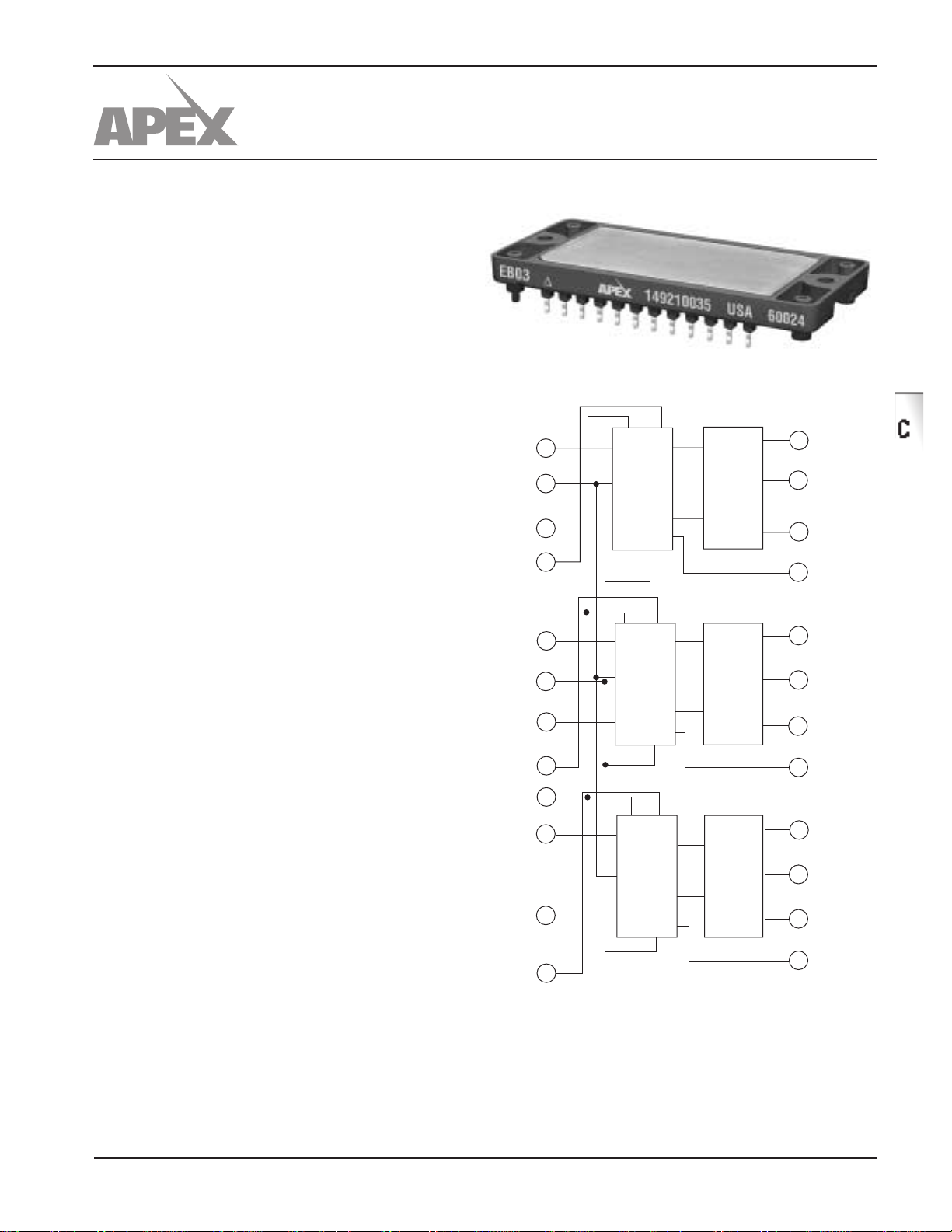
EBO3
12
Hin 1
SD
11
Lin 1
10
Half
Bridge
Driver
FET
Half
Bridge
Output
13
14
15
HV1
OUT1
S1
DESCRIPTION
The EB03 consists of three independent FET half
bridges with drivers. The drivers may be interfaced with
CMOS or HCMOS level logic.
V
,Logic Ground
ss
V
,Logic Supply
dd
V 1
cc
Hin 2
Lin2
V 2
cc
Hin3
Lin 3
V 3
cc
9
8
Half
7
6
5
4
3
2
1
Bridge
Driver
Half
Bridge
Driver
FET
Half
Bridge
Output
FET
Half
Bridge
Output
16
17
18
19
20
21
22
23
24
HVRTN1
HV2
OUT2
S2
HVRTN2
HV3
OUT3
S3
HVRTN3
FIGURE 1. BLOCK DIAGRAM
APEX MICROTECHNOLOGY CORPORATION • TELEPHONE (520) 690-8600 • FAX (520) 888-3329 • ORDERS (520) 690-8601 • EMAIL prodlit@apexmicrotech.com
1
Page 2

EB03
ABSOLUTE MAXIMUM RATINGS
SPECIFICATIONS
ABSOLUTE MAXIMUM RATINGS
MOTOR VOLTAGE SUPPLY, HV 200V
OUTPUT CURRENT, peak 10A
OUTPUT CURRENT, continuous1 5A
GATE SUPPLY VOLTAGE, Vcc 20V
LOGIC SUPPLY VOLTAGE, Vdd 20V
POWER DISSIPATION, internal1 40W
LOGIC INPUT VOLTAGE -0.3V to Vdd + 0.3V
THERMAL RESISTANCE TO CASE3 2.1°C/Watt
TEMPERATURE, pin solder, 10s 300°C
TEMPERATURE, junction2 150°C
TEMPERATURE RANGE, storage –55 to +150°C
OPERATING TEMPERATURE, case –25 to +85°C
SPECIFICATIONS
PARAMETER TEST CONDITIONS MIN TYP MAX UNITS
POSITIVE OUTPUT VOLTAGE I
HV=100V, Fpwm=50kHz, L=100 µH
NEGATIVE OUTPUT VOLTAGE " -1.7 1.9 Volts
POSITIVE EDGE DELAY " 310 n-second
RISETIME " 50 n-second
NEGATIVE EDGE DELAY " 290 n-second
FALLTIME " 50 n-second
PWM FREQUENCY Set by external circuitry 50 kHz
INPUT IMPEDANCE Set by internal resistors 50 k-ohm
INPUT AND OUTPUT SIGNALS
PIN SYMBOL FUNCTION PIN SYMBOL FUNCTION
1 V
2 Lin3 Low drive logic in 3 14 OUT1 Section 1 output
3 Hin3 High drive logic in 3 15 S1 Section 1 source
4 V
5 V
6 Lin2 Low drive logic in 2 18 OUT 2 Section 2 output
7 V
8 Hin2 High drive logic in 2 20 HVRTN2 Section 2 return
9 V
10 Lin1 Low drive logic in 1 22 OUT 3 Section 3 output
11 SD Shut down logic in 23 S3 Section 3 source
12 Hin1 High drive logic in 1 24 HVRTN 3 Section 3 return
3 Gate supply 3 13 HV1 High Voltage supply 1
cc
Logic supply 16 HVRTN1 Section 1 return
dd
2 Gate supply 2 17 HV2 High voltage supply 2
cc
Signal ground 19 S2 Section 2 source
ss
1 Gate supply 1 21 HV3 High voltage supply 3
cc
=5A; Vcc=10.8V , Vdd=5V; 198.1 201.9 Volts
OUT
NOTES: 1. Over Entire Environmental Range.
2. Long term operation at the maximum junction temperature will result in reduced product life. Lower internal temperature by
reducing internal dissipation or using better heatsinking to achieve high MTTF.
3. Each FET.
INPUT
A logic level input independently controls each FET in
the half bridge. A logic level high turns on the FET and
However, input impedance is 50k on all inputs; therefore if
one input is open circuited a high radiated noise level could
spuriously turn on a FET.
low turns it off. A common shut down input turns off all
FETs when high.
All inputs are Schmitt triggers with the upper threshold at
and the lower threshold at 1/3 Vdd. This comfortably
2/3 V
dd
interfaces with CMOS or HCMOS provided that the Vdd for
the logic family and the EB03 are the same.
TTL families may be used if a pull-up to Vcc is added to
the TTL gates driving the EB03, and Vdd for the EB03 is the
same supply as V
An open signal connector pulls the shut down input high
for the TTL family.
cc
OUTPUT
Each output section consists of a switching mode FET half
bridge. Separate HV supply, emitter, and HV return lines are
provided for each section.
The FETs are conservatively rated to carry 5A. At 5A the
saturation voltage is 1.9V maximum.
Each FET has an intrinsic diode connected in anti-parallel.
When switching an inductive load this diode will conduct, and
the drop at 5A will be 1.9V maximum.
and all other inputs low, insuring that all outputs are off.
APEX MICROTECHNOLOGY CORPORATION • 5980 NORTH SHANNON ROAD • TUCSON, ARIZONA 85741 • USA • APPLICATIONS HOTLINE: 1 (800) 546-2739
2
Page 3

PACKAGE
SPECIFICATIONS
PACKAGE SPECIFICATIONS
DIP9 PACKAGE
EB03
WEIGHT: 69 g or 2.4 oz
DIMENSIONS ARE IN INCHES
ALTERNATE UNITS ARE [MM]
APEX MICROTECHNOLOGY CORPORATION • TELEPHONE (520) 690-8600 • FAX (520) 888-3329 • ORDERS (520) 690-8601 • EMAIL prodlit@apexmicrotech.com
3
Page 4

OPERATING
CONSIDERATIONS
EB03
POWER SUPPLY REQUIREMENTS
SUPPLY VOLTAGE MAX CURRENT
HV1 50V to 200V 5A, continuous, 10A peak
HV2 50V to 200V 5A, continuous, 10A peak
HV3 50V to 200V 5A, continuous, 10A peak
Vcc1 10V to 20V 10mA
Vcc2 10V to 20V 10mA
Vcc3 10V to 20V 10mA
Vdd 4.5 to 20V 10mA
HV1, HV2, and HV3 may be used independently, or may
be one supply. Also V
independently or tied together. The V
compatible with the input logic. If a high v oltage logic such as
CMOS is used it may be tied with the V
requires a 5V±10% supply
1, Vcc2, and Vcc3 may be used
cc
supply must be
dd
supplies. HCMOS
cc
SPECIAL CONSIDERATIONS
GENERAL
The EB03 is designed to give the user maximum fl exibility
in a digital or DSP based motion control system. Ther mal,
overvoltage, overcurrent, and crossfi re protection circuits are
part of the user’s design.
Users should read Application Note 1, "General Operating
Considerations;” and Application Note 30, “PWM Basics”
for much useful information in applying this part. These
Application Notes are in the “Power Integrated Circuits Data
Book” and on line at www.apexmicrotech.com.
GROUNDING AND BYPASSING
As in any high power PWM system, grounding and
bypassing are one of the keys to success. The EB03 is
capable of generating 2 kW pulses with 40 n-second rise and
fall times. If improperly grounded or bypassed this can cause
horrible conducted and radiated EMI.
In order to reduce conducted EMI, the EB03 provides a
separate power ground, named HVRTN, f or each high voltage
supply. These grounds are electrically isolated from the logic
ground and each other. This isolation eliminates high current
ground loops. However, more than 5V offset between the
grounds will destroy the EB03. Apex recommends back
to back high current diodes between logic and power
grounds; this will maintain isolation but keep offset at a
safe level. All grounds should tie together at one common
point in the system.
In order to reduce radiated EMI, Apex recommends a 50 µF
or larger capacitor between HV and HVRTN. This capacitor
should be a switching power grade electrolytic capacitor
with ESR rated at 20 kHz. This capacitor should be placed
physically as close to the EB03 as possible.
However, such a capacitor will typically have a few
hundred milli-ohms or so ESR. Therefore, each section
must also be bypassed with a low ESR 1µF or larger
ceramic capacitor.
In order to minimize radiated noise it is necessary to
minimize the area of the loop containing high frequency
current. (The siz e of the antenna.) Theref ore the 1µF ceramic
capacitors should bypass each HV to its return right at
the pins the EB03.
SHOOT THROUGH PROTECTION
Power FETs have a relatively short turn on delay, and a
longer turn off delay. Therefore, if the turn on input to an FET
in a half bridge circuit is applied simultaneously with the turn
off input to the other FET in that half bridge, there will be a time
when both FETs are simultaneoulsy on. This "shoot through
condition" will short the power rails through the FETS, causing
excessive power dissipation and a very high EMI.
T o a void the shoot through condition the turn on of one FET
must be delayed long enough for the other FET in the same
half bridge to have completely turned off.
A delay of at least .5 µ-seconds is required for the EB03. This
delay is required for both the Hin and Lin inputs.
PROTECTION CIRCUITS
The EB03 does not include protection circuits.
However, there is a shut down input which will turn off all
FETs when at logic “1”. This input may be used with user
designed temperature sensing and current sensing circuits
to shut down the FETs in the event of a detected unsafe
condition. This is recommended since the FETs may be
turned off this way even if the normal input logic or DSP
programming is faulty.
START UP CONSIDERATIONS
The lower rail FET in the half bridge must be turned on
for at least 2 µ-seconds to charge the bootstrap capacitor
before the top rail FET can be turned on. This must be done
no more than 330 µ-seconds prior to turning on the top rail
FET. Howev er , a grounded load will also charge the bootstrap
capacitor. Therefore this consideration may be ignored when
driving a grounded load.
An internal fl oating supply is used to enhance the operation
of the bootstrap bias circuit. This allows the top rail FETs to
be held on indefi nitely once turned on.
HEATSINK
The EB03 should be provided with suffi cient heatsink to
dissipate 40 watts when operating at 200V , 5A, 50kHz, 1000pf
load capacitance per section, and 3 sections simultaneously
providing maximum current.
The dissipation is composed of conduction losses (I
up to 9.45 watts per half bridge and switching losses of
about 3.72 watts per half bridge. The conduction losses
are proportional to HV supply voltage, total capacitance,
and switching frequency.
outxVsat
)
This data sheet has been carefully checked and is believed to be reliable, however, no responsibility is assumed for possible inaccuracies or omissions. All specifi ciations are subject to change without notice.
APEX MICROTECHNOLOGY CORPORATION • 5980 NORTH SHANNON ROAD • TUCSON, ARIZONA 85741 • USA • APPLICATIONS HOTLINE: 1 (800) 546-2739
4
EBO3U REV. B JANUARY 2001 © 2001 Apex Microtechnology Corporation
 Loading...