

Datasheet E28F016XS-25, E28F016XS-20, E28F016XS-15, DA28F016XS-15, DA28F016XS-25 Datasheet (Intel Corporation)
...Page 1

E
November 1996 Order Number: 290532-004
n
Effective Zero Wait-State Performance
up to 33 MHz
Synchronous Pipelined Reads
n
SmartVoltage Technology
User-Selectable 3.3V or 5V V
CC
User-Selectable 5V or 12V V
PP
n
0.33 MB/sec Write Transfer Rate
n
Configurable x8 or x16 Operation
n
56-Lead TSOP and SSOP Type I
Package
n
Backwards-Compatible with 28F008SA
Command-Set
n
2 µA Typical Deep Power-Down
n
1 mA Typical Active I
CC
Current in
Static Mode
n
16 Separately-Erasable/Lockable
128-Kbyte Blocks
n
1 Million Erase Cycles per Block
n
State-of-the-Art 0.6 µm ETOX™ IV Flash
Technology
Intel’s 28F016XS 16-Mbit f lash mem ory is a rev olutionary architec ture whic h is the ideal c hoice for des igning
truly revolutionary high-performance products. Combining very high read performance with the intrinsic
nonvolatility of flash memory, the 28F016XS eliminates the traditional redundant memory paradigm of
shadowing code from a slow nonvolatile storage s ource to a faster execution m emory, such as DRAM, f or
improved system performance. The innovative capabilities of the 28F016XS enable the design of directexecute code and mass storage data/file flash memory systems.
The 28F016XS is the highest performance high-density nonvolatile read/program flash memory solution
available today. Its synchronous pipelined read interface, flexible V
CC
and VPP voltages, extended cycling,
fast program and read performance, s ymmetrically-bloc k ed architecture, and selective block loc k i ng provide a
highly flexible memory component suitable for resident flash component arrays on the system board or
SIMMs. The sync hronous pipelined interface and x8/x 16 architecture of the 28F016XS allow easy interf ace
with minimal glue logic to a wide range of processors/buses, providing effective zero wait-state read
performance up to 33 MHz. The 28F016XS’ s dual read voltage allows the same component to operat e at
either 3.3V or 5.0V V
CC
. Programming voltage at 5V VPP minimizes external c ircuitry in minim al-chip, space
critical designs, whi l e t he 12.0V V
PP
option maximizes program/erase performance. Its high read performance
combined with flexible block locking enable both storage and execution of operating systems/application
software and fast acces s to large data tables. The 28F016XS is manuf actured on Intel’s 0.6 µm ETOX IV
process technology.
28F016XS
16-MBIT (1 MBIT x 16, 2 MBIT x 8)
SYNCHRONOUS FLASH MEMORY
Page 2

COPYRIGHT © INTEL CORPORATION, 1996 CG-041493
Information in this document is provided in connection with Intel products. No license, express or implied, by estoppel or
otherwise, to any intellectual property rights is granted by this document. Except as provi ded in Intel ’s Terms and Condi tions of
Sale for such products, Intel assumes no liability whatsoever, and Intel disclaims any express or implied warranty, relating to
sale and/or use of Intel products including liability or warranties relating to fitness for a particular purpose, merchantability, or
infringement of any patent, copyright or other intellectual property right. Intel products are not intended for use in medical, life
saving, or life sustaining applications.
Intel may make changes to specifications and product descriptions at any time, without notice.
The 28F016XS may contain design defects or errors known as errata. Current characterized errata are available upon request.
*Third-party brands and names are the property of their respective owners.
Contact your local Intel sales office or your distributor to obtain the latest specifications and before placing your product order.
Copies of documents which have an ordering number and are referenced in this document, or other Intel literature, may be
obtained from:
Intel Corporation
P.O. Box 7641
Mt. Prospect, IL 60056-7641
or call 1-800-879-4683
Page 3

E 28F016XS FLASH MEMORY
3
CONTENTS
PAGE PAGE
1.0 INTRODUCTION............................................7
1.1 Product Overview ........................................ 7
2.0 DEVICE PINOUT...........................................10
2.1 Lead Descriptions...................................... 12
3.0 MEMORY MAPS........................................... 14
3.1 Extended Status Register Memory Map..... 15
4.0 BUS OPERATIONS, COMMANDS AND
STATUS REGISTER DEFINITIONS.............16
4.1 Bus Operations for Word-Wide Mode
(BYTE# = V
IH
)........................................... 16
4.2 Bus Operations for Byte-Wide Mode
(BYTE# = V
IL
)...........................................17
4.3 28F008SA—Compatible Mode Command
Bus Definitions..........................................18
4.4 28F016XS—Enhanced Command Bus
Definitions.................................................19
4.5 Compatible Status Register .......................20
4.6 Global Status Register............................... 21
4.7 Block Status Register ................................22
4.8 Device Configuration Code........................23
4.9 SFI Configuration Table............................. 23
5.0 ELECTRICAL SPECIFICATIONS .................24
5.1 Absolute Maximum Ratings .......................24
5.2 Capacitance...............................................24
5.3 Transient Input/Output Reference
Waveforms...............................................26
5.4 DC Characteristics (V
CC
= 3.3V)................27
5.5 DC Characteristics (V
CC
= 5.0V)................30
5.6 Timing Nomenclature.................................33
5.7 AC Characteristics—Read Only
Operations................................................34
5.8 AC Characteristics for WE#—Controlled
Write Operations.......................................40
5.9 AC Characteristics for CEX#—Controlled
Write Operations.......................................44
5.10 Power-Up and Reset Timings ..................48
5.11 Erase and Program Performance.............49
6.0 MECHANICAL SPECIFICATIONS................51
APPENDIX A: Device Nomenclature and
Ordering Information..................................53
APPENDIX B: Additional Information...............54
Page 4

28F016XS FLASH MEMORY E
4
REVISION HISTORY
Number Description
-001 Original Version
-002
Removed support of the following features:
• All page buffer operations (read, write, programming, Upload Device Information)
• Command queuing
• Software Sleep and Abort
• Erase all Unlocked Blocks and Two-Byte Write
• RY/BY# Configuration as part of the Device Configuration command
Changed definition of “NC.” Removed “No internal connection to die” from description.
Added “xx” to Upper Byte of Command (Data) Definition in Sections 4.3 and 4.4.
Modified parameters “V” and “I” of Section 5.1 to apply to “NC” pins.
Increased I
PPR
(VPP Read Current) for VPP > VCC to 200 µA at VCC = 3.3V/5.0V.
Changed V
CC
= 5.0V DC Characteristics (Section 5.5) marked with Note 1 to indicate
that these currents are specified for a CMOS rise/fall time (10% to 90%) of <5 ns
and a TTL rise/fall time of <10 ns.
Corrected t
PHCH
(RP# High to CLK) to be a “Min” specification at VCC = 3.3V/5.0V.
Corrected the graphical representation of t
WHCH
and t
EHCH
in Figures 15 and 16.
Increased Typical “Byte/Word Program Times” (t
WHRH1A/tWHRH1B
) for VPP = 5.0V (Sec.
5.13): t
WHRH1A
from 16.5 µs to 29.0 µs and t
WHRH1B
from 24.0 µs to 35.0 µs at VCC =
3.3V
t
WHRH1A
from 11.0 µs to 20.0 µs and t
WHRH1B
from 16.0 µs to 25.0 µs at VCC = 5.0V.
Increased Typical “Block Program Times” (t
WHRH2
/ t
WHRH3
) for VPP = 5.0V (Section 5.13):
t
WHRH2
from 2.2 sec to 3.8 sec and t
WHRH3
from 1.6 sec to 2.4 sec at VCC = 3.3V
t
WHRH2
from 1.6 sec to 2.8 sec and t
WHRH3
from 1.2 sec to 1.7 sec at VCC = 5.0V.
Changed “Time from Erase Suspend Command to WSM Ready” spec name to “Erase
Suspend Latency Time to Read;” Modified typical values and Added Min/Max values
at V
CC
=3.3/5.0V and VPP =5.0/12.0V (Section 5.13).
Minor cosmetic changes throughout document.
-003
Added 3/5# pin to Pinout Configuration (Figure 2), Product Overview (Section 1.1) and
Lead Descriptions (Section 2.1)
Modified Block Diagram (Figure 1): Removed Address Counter; Added 3/5# pin
Added 3/5# pin to Test Conditions of I
CCS
Specifications
Added 3/5# pin (Y) to Timing Nomenclature (Section 5.6)
Removed Note 7 of Section 5.7
Modified Device Configuration Code: Incorporated RY/BY# Configuration (Level Mode
support ONLY)
Modified Power-Up and Reset Timings (Section 5.10) to include 3/5# pin: Removed t
5VPH
and t
3VPH
specifications; Added t
PLYL
, t
PLYH
, t
YLPH
, and t
YHPH
specifications
Added SSOP pinout (Figure 2) and Mechanical Specifications
Corrected TSOP Mechanical Specification A1 from 0.50 mm to 0.050 mm (Section 6.0)
Minor cosmetic changes throughout document.
Page 5

E 28F016XS FLASH MEMORY
5
REVISION HISTORY (Continued)
Number Description
-004
Require all V
CC
Tolerences to be within 5% of Operational Voltage
I
PPES
Is Pushed to 200 µA from 50 Max
I
CCD
Is Pushed to 10 µA from 5 Max
Updated t
AVAV
at 3.3V
Updated t
ELEH
at 3.3V and 5.0V
Page 6

28F016XS FLASH MEMORY E
6
This page intentionally left blank
Page 7

E 28F016XS FLASH MEMORY
7
1.0 INTRODUCTION
The documentation of the Intel 28F016XS Flash
memory device includes this dat asheet, a detailed
user’s manual, a number of applic ation notes and
design tools, all of which are referenced in
Appendix B.
The datasheet is intended to give an overview of
the chip feature-set and of the operating AC/DC
specifications. The
16-Mbit Flash Product Family
User’s Manual
provides complete descriptions of
the user modes, system interface examples and
detailed descriptions of all principles of operation. It
also contains the full list of software algorithm
flowcharts, and a brief sect ion on compatibility with
the Intel 28F008SA.
Significant 28F016XS feature revisions occurred
between datasheet revisions 290532-001 and
290532-002. These revisions center around
removal of the following features:
• All page buffer operations (read, write,
programming, Upload Device Information)
• Command queuing
• Software Sleep and Abort
• Erase all Unlocked Blocks and Two-Byte Write
• RY/BY# Configuration options
In addition, a significant 28F016XS change
occurred between datasheet revis ions 290532-002
and 290532-003. This change centers around the
addition of a 3/5# pin to the device’s pinout
configuration. Figures 2 and 3 show the 3/5# pin
assignment for the TSOP and SSOP Type I
packages.
Intel recommends that all customers obtain the
latest revisions of 28F016XS documentation.
1.1 Product Overview
The 28F016XS is a high-performance, 16-Mbit
(16,777,216-bit) block erasable nonv olatile random
access memory organized as ei ther 1 Mword x 16
or 2 Mbyte x 8, subdivided into even and odd
banks. Address A
1
makes the bank selec tion. The
28F016XS includes sixteen 128-Kbyte (131,072
byte) blocks or sixteen 64-Kword (65,536 word)
blocks. Chip memory maps for x8 and x16 modes
are shown in Figures 4 and 5.
The implementation of a new architecture, with
many enhanced features, will improve the device
operating characteristics and result in greater
product reliability and ease-of-use as compared to
other flash memories. Significant features of the
28F016XS as compared to previous async hronous
flash memories include:
• Synchronous Pipelined Read Interface
• Significantly Improved Read and Program
Performance
• SmartVoltage Technology
Selectable 3.3V or 5.0 V
CC
Selectable 5.0V or 12.0 V
PP
• Block Program/Erase Protection
The 28F016XS’s synchronous pipelined interface
dramatically raises read performance far beyond
previously attainable levels. Addresses are
synchronously latched and data is read from a
28F016XS bank every 30 ns (5V V
CC
, SFI
Configuration = 2). This capability translates to zero
wait-state reads at cloc k rates up to 33 MHz at 5V
V
CC
, after an initial address pipeline fill delay and
assuming even and odd banks within the flash
memory are alternately accessed. Data is latched
and driven valid 20 ns (t
CHQV
) after a rising CLK
edge. The 28F016XS is capable of operating up to
50 MHz (5V V
CC
); its programmable SFI
Configuration enables system design flexibility,
optimizing the 28F016XS to a specific system clock
frequency. See Section 4.9, SFI Configuration
Table, for specific SFI Configurations for given
operating frequencies.
The SFI Configuration optimizes the 28F016XS for
a wide range of system operating frequencies. The
default SFI Configuration is 4, which allows system
boot from the 28F016XS at any frequency up to
50 MHz at 5V V
CC
. After initiating an access, data
is latched and begins driving on the data outputs
after a CLK count corresponding to the SFI
Configuration has elapsed. The 28F016XS will hold
data valid until CE# or OE# is deactiv ated or a CLK
count corresponding to the SFI Configuration for a
subsequent access has elapsed.
The CLK and ADV# inputs, new t o the 28F016XS in
comparison to previous flash memories, control
address latching and device sync hronization during
read operations. The CLK input controls t he device
latencies, times out the SFI Configuration counter
and synchronizes data output s. ADV# indic ates the
presence of a valid address on the 28F016XS
Page 8

28F016XS FLASH MEMORY E
8
address inputs. During read operations, address es
are latched and accesses are i nitiated on a rising
CLK edge in conjunction with ADV# low. Both CLK
and ADV# are ignored by the 28F016XS during
command/data write sequences.
The 28F016XS incorporates SmartVoltage
technology, providing V
CC
operation at both 3.3V
and 5.0V and program and erase capability at
V
PP
= 12.0V or 5.0V. Operating at VCC = 3.3V, the
28F016XS consumes less than one half the power
consumption at 5.0V V
CC
, while 5.0V VCC provides
highest read performance capability. V
PP
operation
at 5.0V eliminates the need for a separate 12.0V
converter, while the V
PP
= 12.0V option maximizes
program/erase performance. In addition to the
flexible program and erase voltages , the dedicated
V
PP
gives complete code protection with VPP ≤
V
PPLK
.
A 3/5# input pin configures the device’s internal
circuitry for optimal 3.3V or 5.0V read/program
operation.
A Command User Interface (CUI) serves as the
system interface between the microprocessor or
microcontroller and the internal memory operation.
Internal Algorithm Automation allows program and
block erase operations to be ex ecut ed using a TwoWrite command sequence to the CUI in the s ame
way as the 28F008SA 8-Mbit FlashFile™ memory.
Software locking of memory blocks is an added
feature of the 28F016XS as compared to the
28F008SA. The 28F016XS provides selectable
block locking to protec t c ode or data s uch as direc texecutable operating systems or application code.
Each block has an associated nonvolatile lock-bit
which determines the lock status of the block. In
addition, the 28F016XS has a mas ter Write Protec t
pin (WP#) which prevents any modifications to
memory blocks whose lock-bits are set.
Writing of memory data is perf ormed in either byte
or word increments, typic ally within 6 µs at 12.0V
V
PP
, which is a 33% improvement over the
28F008SA. A block erase operation erases one of
the 16 blocks in typically 1.2 sec, independent of
the other blocks.
Each block can be written and erased a minimum of
100,000 cycles. Systems can achieve one million
Block Erase Cycles by providing wear-leveling
algorithms and graceful block retirement. These
techniques have already been employed in many
flash file systems and hard disk drive designs.
All operations are started by a sequence of Write
commands to the device. Three Status Registers
(described in detail later in this datasheet) and a
RY/BY# output pin provide information on the
progress of the requested operation.
The following Status Regist ers are used to prov ide
device and WSM operation information to the user:
• A Compatible Status Register (CSR) which is
100% compatible with the 28F008SA FlashFile
memory Status Regist er. The CSR, when used
alone, provides a straightforward upgrade
capability to the 28F016XS from a 28F008SAbased design.
• A Global Status Register (GSR) which also
informs the system of overall Write State
Machine (WSM) status.
• 16 Block Status Registers (BSRs) which
provide block-specific status information such
as the block lock-bit status.
The GSR and BSR memory maps for Byte-Wide
and Word-Wide modes are shown in Figures 5
and 6.
The 28F016XS incorporates an open drain RY/BY #
output pin. This feature allows the user to OR-tie
many RY/BY# pins toget her in a multiple memory
configuration such as a Resident Flash Array.
The 28F016XS also incorporates a dual chipenable function with two input pi ns, CE
0
# and CE1#.
These pins have exactly the same functionality as
the regular chip-enable pin, CE#, on the 28F008SA .
For minimum chip designs, CE
1
# may be tied to
ground and system logic may use CE
0
# as the chip
enable input. The 28F016XS uses the logical
combination of these two signals to enable or
disable the entire chip. Bot h CE
0
# and CE1# must
be active low to enable the device. If either one
becomes inactive, the chip will be disabled. This
feature, along with the open drain RY/BY# pin,
allows the system designer to reduce the number of
control pins used in a large array of 16-Mbit
devices.
Page 9
E 28F016XS FLASH MEMORY
9
4/15/97 9:41 AM 9053204.DOC
INTEL CONFIDENTIAL
(until publication date)
Output
Buffer
Output
Buffer
Input
Buffer
Input
Buffer
I/O L ogic
ID
Register
CSR
ESRs
Data
Comparator
CUI
WSM
Program/Erase
Voltage Sw itch
Address
Register
Input
Buffer
Output Multiplexer
GND
DQ
8-15
DQ
0-7
CE #
CE #
OE#
WE#
WP#
RP#
V
CC
V
RY/BY#
PP
A
0-20
Data
Register
1
0
CLK
ADV#
Y Gating/Sensing
Odd Bank
Y Gating/Sensing
Even Bank
Y
Decoder
X
Decoder
Even Address Latch
Y
Decoder
X
Decoder
Odd Address Latch
Block 0 128-Kbyte
Block 1 128-Kbyte
Block 14 128-Kbyte
Block 15 128-Kbyte
BYTE#
3/5#
3/5#
0532_01
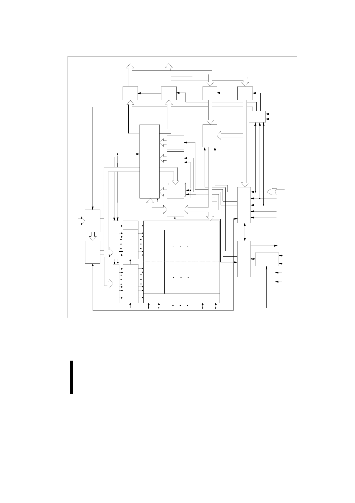
Figure 1. 28F016XS Block Diagram
Architectural Evolution Includes Synchronous Pipelined Read Interface,
SmartVoltage Technology, and Extended Status Registers
Page 10
28F016XS FLASH MEMORY E
10
The BYTE# pin allows either x8 or x16
read/programs to the 28F016XS. BYTE# at logic
low selects 8-bit mode with address A
0
selecting
between low byte and high byte. On the ot her hand,
BYTE# at logic high enables 16-bit operation with
address A
1
becoming the lowest order address and
address A
0
is not used (don’t care). A devic e block
diagram is shown in Figure 1.
The 28F016XS incorporates an Automatic Power
Saving (APS) feature, which substantially reduces
the active current when the device is in st atic mode
of operation (addresses not switching). In APS
mode, the typical I
CC
current is 1 mA at 5.0V (3 mA
at 3.3V).
A deep power-down mode of operation is invoked
when the RP# (called PWD# on the 28F008SA) pin
transitions low. This mode brings the device power
consumption to less than 2.0 µA, typically, and
provides additional write protec tion by acting as a
device reset pin during power transitions. A reset
time of 300 ns (5V V
CC
) is required from RP#
switching high before latching an address i nto the
28F016XS. In the deep power-down state, the
WSM is reset (any current operation will abort) and
the CSR, GSR and BSR registers are cleared.
A CMOS standby mode of operation is enabled
when either CE
0
# or CE1# transitions high and RP#
stays high with all input control pins at CMOS
levels. In this m ode, the device typically draws an
I
CC
standby current of 70 µA at 5V VCC.
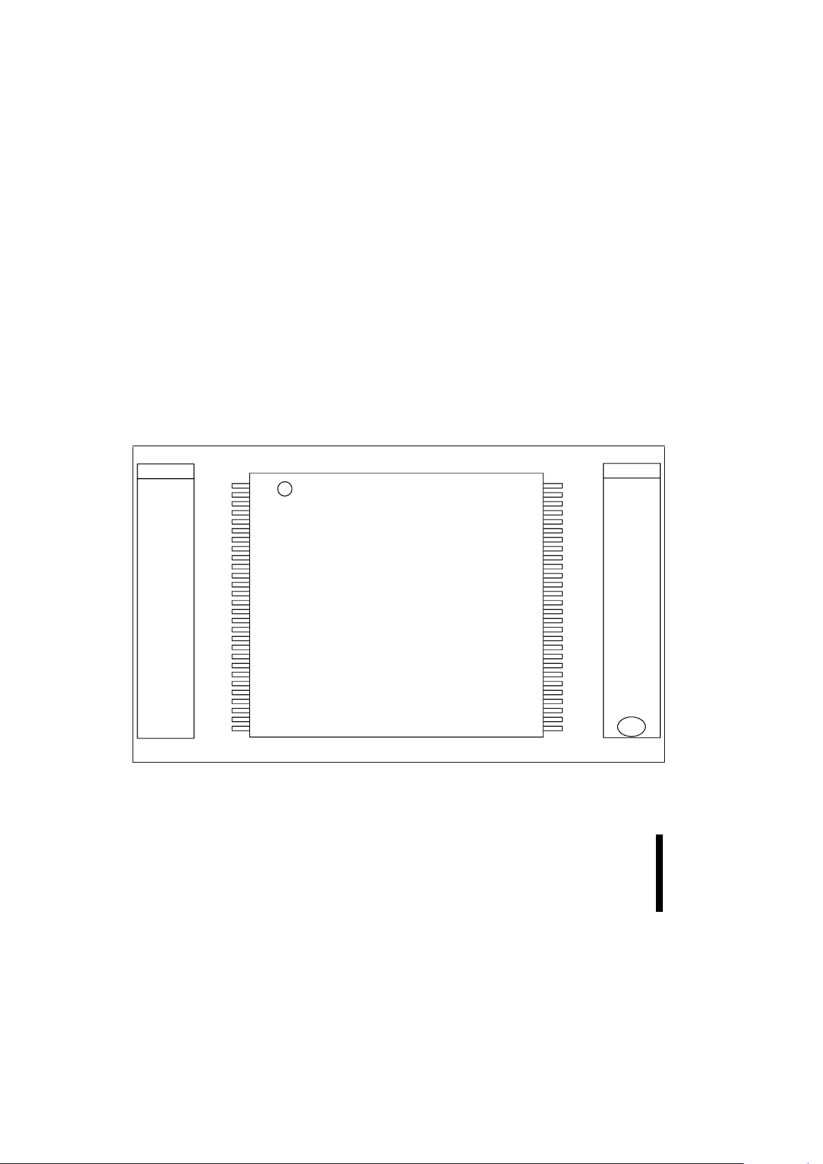
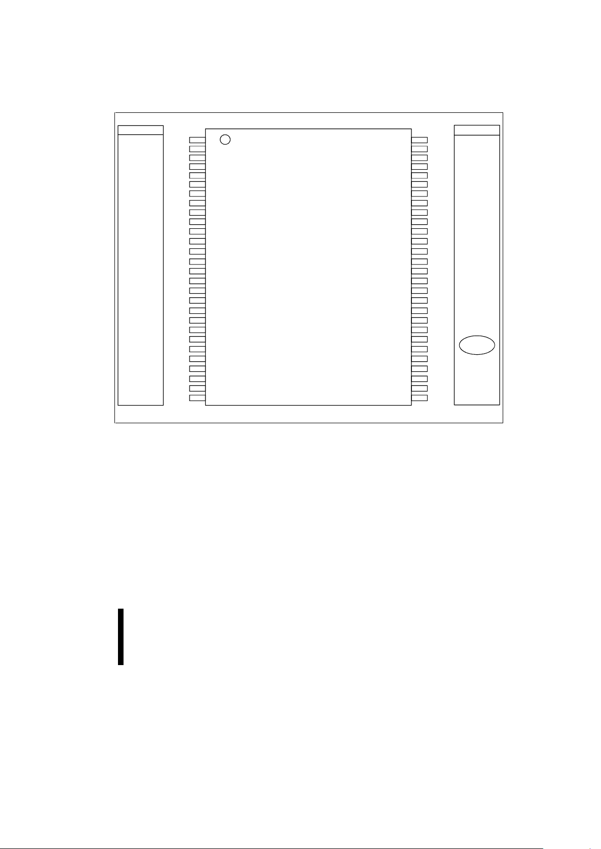
The 28F016XS is available in 56-Lead, 1.2 mm
thick, 14 mm x 20 mm TSOP and 1.8 mm thick, 16
mm x 23.7 mm SSOP Ty pe I packages. The form
factor and pinout of these t wo packages allow for
very high board layout densities.
2.0 DEVICE PINOUT
The 28F016XS is pinout compatible with the
28F016SA/SV 16-Mbit FlashFile memory components, providing a performance upgrade path t o
the 28F016XS. The 28F016XS 56-Lead TSOP and
SSOP pinout configurati ons are shown in Fi gures 2
and 3.
CE #
1
28F016SA/SV
1
2
3
4
5
6
7
8
9
10
11
12
13
14
15
16
17
18
19
20
21
22
23
24
25
26
27
28
29
30
31
32
33
34
56
55
53
54
52
51
50
49
48
47
46
45
44
43
42
41
40
39
38
37
36
35
E28F016XS
56-LEAD TSOP PINOUT
14 mm x 20 mm
TOP VIEW
3/5#
3/5#
NC
WP#
WE#
OE#
RY/BY#
GND
GND
DQ
7
DQ
14
DQ
6
DQ
13
DQ
5
DQ
12
DQ
4
DQ
11
DQ
3
DQ
10
BYTE#
ADV#
CLK
DQ
2
DQ
9
DQ
1
DQ
8
DQ
0
A
0
DQ
15
V
CC
V
CC
A
17
A
18
A
19
A
20
V
CC
A
15
A
14
A
13
A
12
V
PP
RP#
A
11
A
10
A
9
GND
A
7
A
6
A
5
A
4
A
3
A
2
A
1
A
16
28F016SA/SV
A
8
WP#
WE#
OE#
RY/BY#
GND
GND
DQ
7
DQ
14
DQ
6
DQ
13
DQ
5
DQ
12
DQ
4
DQ
11
DQ
3
DQ
10
BYTE#
NC
NC
DQ
2
DQ
9
DQ
1
DQ
8
DQ
0
A
0
DQ
15
V
CC
V
CC
CE #
0
NC
A
17
A
18
A
19
A
20
V
CC
A
15
A
14
A
13
A
12
V
PP
RP#
A
11
A
10
A
9
A
8
GND
A
7
A
6
A
5
A
4
A
3
A
2
A
1
CE #
1
A
16
CE #
0
0532_02
Figure 2. 28F016XS 56-Lead TSOP Pinout Configuration Shows Compatibility with
the 28F016SA/SV, Allowing for Easy Performance Upgrades from Existing 16-Mbit Designs
Page 11
E 28F016XS FLASH MEMORY
11
4/15/97 9:41 AM 9053204.DOC
INTEL CONFIDENTIAL
(until publication date)
NC
RY/BY#
WE#
WP#
OE#
GND
DA28F016XS
56-LEAD SSOP
STANDARD PINOUT
16 mm x 23.7 mm
TOP VIEW
56
55
54
53
52
51
50
49
48
47
46
45
44
43
42
41
40
39
38
37
36
35
34
33
32
31
30
29
1
2
3
4
5
6
7
8
9
10
11
12
13
14
15
16
17
18
19
20
21
22
23
24
25
26
27
28
A
12
CE #
0
A
13
A
14
A
15
CE #
1
A
18
A
17
A
16
V
CC
A
20
A
19
V
CC
DQ
13
DQ
5
DQ
4
DQ
12
DQ
6
DQ
14
DQ
7
DQ
15
RP#
GND
BYTE#
ADV#
CLK
GND
DQ
10
DQ
3
DQ
11
DQ
0
A
0
DQ
8
DQ
1
DQ
9
V
CC
A
8
A
7
A
6
A
5
A
4
A
3
A
2
A
1
A
9
A
10
A
11
V
PP
3/5#
28F016SA/SV
3/5#
NC
WE#
WP#
OE#
GND
A
12
CE #
0
A
13
A
14
A
15
CE #
1
A
20
A
19
A
18
A
17
A
16
V
CC
V
CC
RY/BY#
DQ
13
DQ
5
DQ
12
DQ
4
DQ
6
DQ
14
DQ
7
DQ
15
28F016SA/SV
RP#
GND
BYTE#
NC
NC
GND
DQ
10
DQ
3
DQ
11
DQ
0
DQ
8
DQ
1
DQ
9
V
CC
A
8
A
10
A
11
V
PP
DQ
2
DQ
2
A
7
A
4
A
3
A
2
A
1
A
9
A
5
A
6
A
0
XS_SSOP
Figure 3. 28F016XS 56-Lead SSOP Pinout Configuration Shows Compatibility with the 28F016SA/SV,
Allowing for Easy Performance Upgrades from Existing 16-Mbit Designs
Page 12
28F016XS FLASH MEMORY E
12
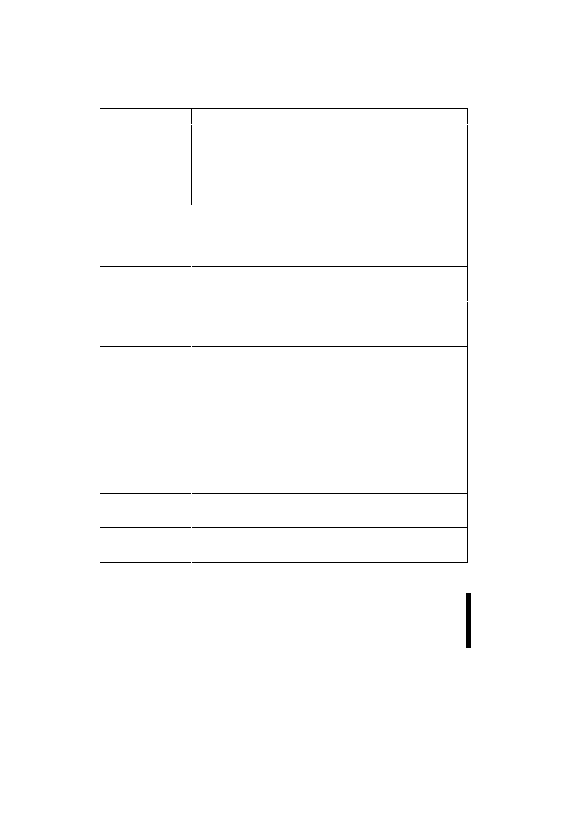
2.1 Lead Descriptions
Symbol Type Name and Function
A
0
INPUT BYTE-SELECT ADDRESS: Selects between high and low byte when device is
in x8 mode. This address is latched in x8 data programs and ignored in x16
mode (i.e., the A
0
input buffer is turned off when BYTE# is high).
A
1
INPUT BANK-SELECT ADDRESS: Selects an even or odd bank in a selected block.
A 128-Kbyte block is subdivided into an even and odd bank. A
= 0 selects the
even bank and A
= 1 selects the odd bank, in both byte-wide mode and word-
wide mode device configurations.
A2–A
16
INPUT WORD-SELECT ADDRESSES: Select a word within one 128-Kbyte block.
Address A
and A
7–16
select 1 of 2048 rows, and A
2–6
select 16 of 512
columns. These addresses are latched during both data reads and programs.
A17–A
20
INPUT BLOCK-SELECT ADDRESSES: Select 1 of 16 erase blocks. These
addresses are latched during data programs, erase and lock-block operations.
DQ0–DQ
7
INPUT/
OUTPUT
LOW-BYTE DATA BUS: Inputs data and commands during CUI write cycles.
Outputs array, identifier or status data in the appropriate read mode. Floated
when the chip is de-selected or the outputs are disabled.
DQ8–DQ
15
INPUT/
OUTPUT
HIGH-BYTE DATA BUS: Inputs data during x16 data program operations.
Outputs array or identifier data in the appropriate read mode; not used for
Status Register reads. Outputs floated when the chip is de-selected, the
outputs are disabled (OE# = V
IH
) or BYTE# is driven active.
CE0#, CE1# INPUT
CHIP ENABLE INPUTS: Activate the device’s control logic, input buffers,
decoders and sense amplifiers. With either CE
0
# or CE1# high, the device is
de-selected and power consumption reduces to standby levels upon
completion of any current data program or erase operations. Both CE
0
# and
CE
1
# must be low to select the device.
All timing specifications are the same for both signals. Device Selection occurs
with the latter falling edge of CE
0
# or CE1#. The first rising edge of CE0# or
CE
1
# disables the device.
RP# INPUT
RESET/POWER-DOWN: RP# low places the device in a deep power-down
state. All circuits that consume static power, even those circuits enabled in
standby mode, are turned off. When returning from deep power-down, a
recovery time of t
PHCH
is required to allow these circuits to power-up.
When RP# goes low, the current WSM operation is terminated, and the device
is reset. All Status Registers return to ready, clearing all status flags. Exit from
deep power-down places the device in read array mode.
OE# INPUT
OUTPUT ENABLE: Drives device data through the output buffers when low.
The outputs float to tri-state off when OE# is high. CEx# overrides OE#, and
OE# overrides WE#.
WE# INPUT WRITE ENABLE: Controls access to the CUI, Data Register and Address
Latch. WE# is active low, and latches both address and data (command or
array) on its rising edge.
Page 13

E 28F016XS FLASH MEMORY
13
4/15/97 9:41 AM 9053204.DOC
INTEL CONFIDENTIAL
(until publication date)
2.1 Lead Descriptions (Continued)
Symbol Type Name and Function
CLK INPUT CLOCK: Provides the fundamental timing and internal operating frequency.
CLK latches input addresses in conjunction with ADV#, times out the desired
output SFI Configuration as a function of the CLK period, and synchronizes
device outputs. CLK can be slowed or stopped with no loss of data or
synchronization. CLK is ignored during program operations.
ADV# INPUT ADDRESS VALID: Indicates that a valid address is present on the address
inputs. ADV# low at the rising edge of CLK latches the address on the address
inputs into the flash memory and initiates a read access to the even or odd
bank depending on the state of A
1
. ADV# is ignored during program operations.
RY/BY# OPEN
DRAIN
OUTPUT
READY/BUSY: Indicates status of the internal WSM. When low, it indicates
that the WSM is busy performing an operation. RY/BY# high indicates that the
WSM is ready for new operations, erase is suspended, or the device is in deep
power-down mode. This output is always active (i.e., not floated to tri-state off
when OE# or CE
0
#, CE1# are high).
WP# INPUT WRITE PROTECT: Erase blocks can be locked by writing a nonvolatile lock-bit
for each block. When WP# is low, those locked blocks as reflected by the
Block-Lock Status bits (BSR.6), are protected from inadvertent data programs
or erases. When WP# is high, all blocks can be written or erased regardless of
the state of the lock-bits. The WP# input buffer is disabled when RP#
transitions low (deep power-down mode).
BYTE# INPUT
BYTE ENABLE: BYTE# low places device in x8 mode. All data is then input or
output on DQ
0–7
, and DQ
8
–15
float. Address A0 selects between the high and
low byte. BYTE# high places the device in x16 mode, and turns off the A
0
input
buffer. Address A
1
then becomes the lowest order address.
3/5# INPUT 3.3/5.0 VOLT SELECT: 3/5# high configures internal circuits for 3.3V
operation. 3/5# low configures internal circuits for 5.0V operation.
NOTE:
Reading the array with 3/5# high in a 5.0V system could damage the device.
Reference the power-up and reset timings (Section 5.10) for 3/5# switching
delay to valid data.
V
PP
SUPPLY PROGRAM/ERASE POWER SUPPLY (12.0V ± 0.6V, 5.0V ± 0.5V) :
For erasing memory array blocks or writing words/bytes into the flash array.
V
= 5.0V ± 0.5V eliminates the need for a 12.0V converter, while the 12.0V ±
0.6V option maximizes program/erase performance.
Successful completion of program and erase attempts is inhibited with V
at
or below 1.5V. Program and erase attempts with V
between 1.5V and 4.5V,
between 5.5V and 11.4V, and above 12.6V produce spurious results and
should not be attempted.
V
CC
SUPPLY
DEVICE POWER SUPPLY (3.3V ± 5%, 5.0V ± 5%):
To switch 3.3V to 5.0V (or vice versa), first ramp V
CC
down to GND, and then
power to the new V
CC
voltage. Do not leave any power pins floating.
Page 14
28F016XS FLASH MEMORY E
14
2.1 Lead Descriptions (Continued)
Symbol Type Name and Function
GND SUPPLY
GROUND FOR ALL INTERNAL CIRCUITRY:
Do not leave any ground pins floating.
NC
NO CONNECT:
Lead may be driven or left floating.
3.0 MEMORY MAPS
0
1
2
3
4
5
6
7
8
9
10
11
12
13
14
15
128-Kbyte Block
128-Kbyte Block
128-Kbyte Block
128-Kbyte Block
128-Kbyte Block
128-Kbyte Block
128-Kbyte Block
128-Kbyte Block
128-Kbyte Block
128-Kbyte Block
128-Kbyte Block
128-Kbyte Block
128-Kbyte Block
128-Kbyte Block
128-Kbyte Block
128-Kbyte Block
x8 Mode
000000
1FFFFF
1BFFFF
1C0000
1DFFFF
1E0000
19FFFF
1A0000
17FFFF
180000
15FFFF
160000
13FFFF
140000
11FFFF
120000
0FFFFF
100000
0DFFFF
0E0000
0BFFFF
0C0000
09FFFF
0A0000
07FFFF
080000
05FFFF
060000
03FFFF
040000
01FFFF
020000
A
20-0
0532_03
Figure 4. 28F016XS Memory Map
(Byte-Wide Mode)
64-Kword Block
64-Kword Block
64-Kword Block
64-Kword Block
64-Kword Block
64-Kword Block
64-Kword Block
64-Kword Block
64-Kword Block
64-Kword Block
64-Kword Block
64-Kword Block
64-Kword Block
64-Kword Block
64-Kword Block
64-Kword Block
0
1
2
3
4
5
6
7
8
9
10
11
12
13
14
15
x16 Mode
FFFFF
00000
EFFFF
F0000
DFFFF
E0000
CFFFF
D0000
BFFFF
C0000
AFFFF
B0000
9FFFF
A0000
8FFFF
90000
7FFFF
80000
6FFFF
70000
5FFFF
60000
4FFFF
50000
3FFFF
40000
2FFFF
30000
1FFFF
20000
0FFFF
10000
A
20-1
0532_04
Figure 5. 28F016XS Memory Map
(Word-Wide Mode)
Page 15
E 28F016XS FLASH MEMORY
15
4/15/97 9:41 AM 9053204.DOC
INTEL CONFIDENTIAL
(until publication date)
3.1 Extended Status Register Memory Map
1E0004H
1E0003H
1E0002H
1E0000H
1E0001H
1E0005H
1E0006H
000004H
000003H
000002H
000000H
000001H
000006H
000005H
01FFFFH
RESERVED
GSR
RESERVED
BSR 0
RESERVED
RESERVED
RESERVED
A
20-0
x8 Mode
.
.
.
RESERVED
1FFFFFH
RESERVED
GSR
RESERVED
BSR 15
RESERVED
RESERVED
0532_05
Figure 6. Extended Status Register Memory
Map (Byte-Wide Mode)
00002H
00000H
00001H
00003H
0FFFFH
RESERVED
GSR
RESERVED
BSR 0
RESERVED
RESERVED
RESERVED
F0002H
F0000H
F0001H
F0003H
RESERVED
GSR
RESERVED
BSR 15
RESERVED
RESERVED
A
20-1
x16 Mode
.
.
.
RESERVED
FFFFFH
0532_06
Figure 7. Extended Status Register Memory
Map (Word-Wide Mode)
Page 16
28F016XS FLASH MEMORY E
16
4.0 BUS OPERATIONS, COMMANDS AND STATUS REGISTER DEFINITIONS
4.1 Bus Operations for Word-Wide Mode (BYTE# = V
IH
)
Mode Notes RP# CE
0–1
# OE# WE# ADV# CLK A1DQ
0–15
RY/BY#
Latch Read
Address
1,9,10 V
IH
V
IL
XVIHV
IL
↑ XX X
Inhibit
Latching
Read Address
1,9 V
IH
V
IL
XVIHV
IH
↑ XX X
Read 1,2,7,9 V
IH
V
IL
V
IL
V
IH
X ↑ XD
OUT
X
Output
Disable
1,6,7,9 V
IH
V
IL
V
IH
V
IH
X X X High Z X
Standby 1,6,7,9 V
IH
V
IL
XXXXXHigh Z X
Deep
Power-Down
1,3 V
IL
XXXXXXHigh Z V
OH
ManufacturerID1,4,9 V
IH
V
IL
V
IL
V
IH
X ↑ V
IL
0089H V
OH
Device ID 1,4,8,9 V
IH
V
IL
V
IL
V
IH
X ↑ V
IH
66A8H V
OH
Write 1,5,6,9 V
IH
V
IL
V
IH
V
IL
XXXDINX
NOTES:
1. X can be V
IH
or V
IL
for address or control pins except for RY/BY#, which is either V
OL
or V
OH
, or High Z or D
OUT
for data
pins depending on whether or not OE# is active.
2. RY/BY# output is open drain. When the WSM is ready, Erase is suspended, or the device is in deep power-down mode,
RY/BY# will be at V
OH
if it is tied to V
CC
through a resistor. RY/BY# at V
OH
is independent of OE# while a WSM operation
is in progress.
3. RP# at GND ± 0.2V ensures the lowest deep power-down current.
4. A
0
and A1 at VIL provide device manufacturer codes in x8 and x16 modes respectively. A0 and A1 at VIH provide device ID
codes in x8 and x16 modes respectively. All other addresses are set to zero.
5. Commands for erase, data program, or lock-block operations can only be completed successfully when V
PP
= V
PPH1
or
V
PP
= V
PPH2
.
6. While the WSM is running, RY/BY# stays at V
OL
until all operations are complete. RY/BY# goes to VOH when the WSM is
not busy or in erase suspend mode.
7. RY/BY# may be at V
OL
while the WSM is busy performing various operations (for example, a Status Register read during a
write operation).
8. The 28F016XS shares an identical device identifier with the 28F016XD.
9. CE
0–1
# at VIL is defined as both CE0# and CE1# low, and CE
0–1
# at VIH is defined as either CE0# or CE1# high.
10. Addresses are latched on the rising edge of CLK in conjunction with ADV# low. Address A
1
= 0 selects the even bank and
A
1
= 1 selects the odd bank, in both byte-wide mode and word-wide mode device configurations.
Page 17
E 28F016XS FLASH MEMORY
17
4/15/97 9:41 AM 9053204.DOC
INTEL CONFIDENTIAL
(until publication date)
4.2 Bus Operations for Byte-Wide Mode (BYTE# = VIL)
Mode Notes RP# CE
0–1
# OE# WE# ADV# CLK A
0
DQ
0–7
RY/BY#
Latch Read
Address
1,9,10 V
IH
V
IL
XVIHV
IL
↑ XX X
Inhibit
Latching
Read Address
1,9 V
IH
V
IL
XVIHV
IH
↑ XX X
Read 1,2,7,9 V
IH
V
IL
V
IL
V
IH
X ↑ XD
OUT
X
Output
Disable
1,6,7,9 V
IH
V
IL
V
IH
V
IH
X X X High Z X
Standby 1,6,7,9 V
IH
V
IH
XXXXXHigh Z X
Deep
Power-Down
1,3 V
IL
XXXXXXHigh Z V
OH
ManufacturerID1,4,9 V
IH
V
IL
V
IL
V
IH
X ↑ V
IL
89H V
OH
Device ID 1,4,8,9 V
IH
V
IL
V
IL
V
IH
X ↑ V
IH
A8H V
OH
Write 1,5,6,9 V
IH
V
IL
V
IH
V
IL
XXXDINX
NOTES:
1. X can be V
IH
or V
IL
for address or control pins except for RY/BY#, which is either V
OL
or V
OH
, or High Z or D
OUT
for data
pins depending on whether or not OE# is active.
2. RY/BY# output is open drain. When the WSM is ready, Erase is suspended, or the device is in deep power-down mode,
RY/BY# will be at V
OH
if it is tied to V
CC
through a resistor. RY/BY# at V
OH
is independent of OE# while a WSM operation
is in progress.
3. RP# at GND ± 0.2V ensures the lowest deep power-down current.
4. A
0
and A1 at VIL provide device manufacturer codes in x8 and x16 modes respectively. A0 and A1 at VIH provide device ID
codes in x8 and x16 modes respectively. All other addresses are set to zero.
5. Commands for erase, data program, or lock-block operations can only be completed successfully when V
PP
= V
PPH1
or
V
PP
= V
PPH2
.
6. While the WSM is running, RY/BY# stays at V
OL
until all operations are complete. RY/BY# goes to VOH when the WSM is
not busy or in erase suspend mode.
7. RY/BY# may be at V
OL
while the WSM is busy performing various operations (for example, a Status Register read during a
program operation).
8. The 28F016XS shares an identical device identifier with the 28F016XD.
9. CE
0–1
# at VIL is defined as both CE0# and CE1# low, and CE
0–1
# at VIH is defined as either CE0# or CE1# high.
10. Addresses are latched on the rising edge of CLK in conjunction with ADV# low. Address A
1
= 0 selects the even bank and
A
1
= 1 selects the odd bank, in both byte-wide mode and word-wide mode device configurations.
Page 18

28F016XS FLASH MEMORY E
18
4.3 28F008SA—Compatible Mode Command Bus Definitions
First Bus Cycle Second Bus Cycle
Command Notes Oper Addr Data
(4)
Oper Addr Data
(4)
Read Array Write X xxFFH Read AA AD
Intelligent Identifier 1 Write X xx90H Read IA ID
Read Compatible Status Register 2 Write X xx70H Read X CSRD
Clear Status Register 3 Write X xx50H
Program Write X xx40H Write PA PD
Alternate Program Write X xx10H Write PA PD
Block Erase/Confirm Write X xx20H Write BA xxD0H
Erase Suspend/Resume Write X xxB0H Write X xxD0H
ADDRESS DATA
AA = Array Address AD = Array Data
BA = Block Address CSRD = CSR Data
IA = Identifier Address ID = Identifier Data
PA = Program Address PD = Program Data
X = Don’t Care
NOTES:
1. Following the Intelligent Identifier command, two read operations access the manufacturer and device signature codes.
2. The CSR is automatically available after device enters data program, erase, or suspend operations.
3. Clears CSR.3, CSR.4 and CSR.5. Also clears GSR.5 and all BSR.5, BSR.4 and BSR.2 bits. See Status Register
definitions.
4. The upper byte of the data bus (D
8–15
) during command writes is a “Don’t Care” in x16 operation of the device.
Page 19

E 28F016XS FLASH MEMORY
19
4/15/97 9:41 AM 9053204.DOC
INTEL CONFIDENTIAL
(until publication date)
4.4 28F016XS—Enhanced Command Bus Definitions
First Bus Cycle Second Bus Cycle
Command Notes Oper Addr Data
(4)
Oper Addr Data
(4)
Read Extended Status Register 1 Write X xx71H Read RA GSRD
BSRD
Lock Block/Confirm Write X xx77H Write BA xxD0H
Upload Status Bits/Confirm 2 Write X xx97H Write X xxD0H
Device Configuration 3 Write X xx96H Write X DCCD
ADDRESS DATA
BA = Block Address AD = Array Data
RA = Extended Register Address BSRD = BSR Data
PA = Program Address GSRD = GSR Data
X = Don’t Care DCCD = Device Configuration Code Data
NOTES:
1. RA can be the GSR address or any BSR address. See Figures 5 and 6 for Extended Status Register memory maps.
2. Upon device power-up, all BSR lock-bits come up locked. The Upload Status Bits command must be written to reflect the
actual lock-bit status.
3. This command sets the SFI Configuration allowing the device to be optimized for the specific sytem operating frequency.
4. The upper byte of the Data bus (D
8–15
) during command writes is a “Don’t Care” in x16 operation of the device.
Page 20

28F016XS FLASH MEMORY E
20
4.5 Compatible Status Register
WSMS ESS ES DWS VPPS R R R
76543210
NOTES:
CSR.7 = WRITE STATE MACHINE STATUS
1 = Ready
0 = Busy
RY/BY# output or WSMS bit must be checked to
determine completion of an operation (erase,
erase suspend, or data program) before the
appropriate Status bit (ESS, ES or DWS) is
checked for success.
CSR.6 = ERASE-SUSPEND STATUS
1 = Erase Suspended
0 = Erase In Progress/Completed
CSR.5 = ERASE STATUS
1 = Error In Block Erasure
0 = Successful Block Erase
If DWS and ES are set to “1” during an erase
attempt, an improper command sequence was
entered. Clear the CSR and attempt the
operation again.
CSR.4 = DATA WRITE STATUS
1 = Error in Data Program
0 = Data Program Successful
CSR.3 = V
STATUS
1 = V
Error Detect, Operation Abort
0 = V
PP
OK
The VPPS bit, unlike an A/D converter, does not
provide continuous indication of V
level. The
WSM interrogates V
’s level only after the Data
Program or Erase command sequences have
been entered, and informs the system if V
has
not been switched on. VPPS is not guaranteed to
report accurate feedback between V
(max)
and V
(min), between V
(max) and
V
PPH2
(min), and above V
PPH2
(max).
CSR.2–0 = RESERVED FOR FUTURE ENHANCEMENTS
These bits are reserved for future use; mask them out when polling the CSR.
Page 21

E 28F016XS FLASH MEMORY
21
4/15/97 9:41 AM 9053204.DOC
INTEL CONFIDENTIAL
(until publication date)
4.6 Global Status Register
WSMS OSS DOS R R R R R
76543210
NOTES:
GSR.7 = WRITE STATE MACHINE STATUS
1 = Ready
0 = Busy
RY/BY# output or WSMS bit must be checked to
determine completion of an operation (block lock,
suspend, Upload Status Bits, erase or data
program) before the appropriate Status bit (OSS
or DOS) is checked for success.
GSR.6 = OPERATION SUSPEND STATUS
1 = Operation Suspended
0 = Operation in Progress/Completed
GSR.5 = DEVICE OPERATION STATUS
1 = Operation Unsuccessful
0 = Operation Successful or Currently
Running
GSR.4–0 = RESERVED FOR FUTURE ENHANCEMENTS
These bits are reserved for future use; mask them out when polling the GSR.
Page 22

28F016XS FLASH MEMORY E
22
4.7 Block Status Register
BS BLS BOS R R VPPS VPPL R
76543210
NOTES:
BSR.7 = BLOCK STATUS
1 = Ready
0 = Busy
RY/BY# output or BS bit must be checked to
determine completion of an operation (block lock,
suspend, erase or data program) before the
appropriate Status bits (BOS, BLS) is checked
for success.
BSR.6 = BLOCK LOCK STATUS
1 = Block Unlocked for Program/Erase
0 = Block Locked for Program/Erase
BSR.5 = BLOCK OPERATION STATUS
1 = Operation Unsuccessful
0 = Operation Successful or
Currently Running
BSR.2 = V
STATUS
1 = V
Error Detect, Operation Abort
0 = V
PP
OK
BSR.1 = V
LEVEL
1 = V
Detected at 5.0V ± 10%
0 = V
Detected at 12.0V ± 5%
BSR.1 is not guaranteed to report accurate
feedback between the V
and V
voltage
ranges. Programs and erases with V
between
V
(max) and V
(min), between
V
(max) and V
(min), and above
V
(max) produce spurious results and should
not be attempted.
BSR.4,3,0 = RESERVED FOR FUTURE ENHANCEMENTS
These bits are reserved for future use; mask them out when polling the BSRs.
Page 23

E 28F016XS FLASH MEMORY
23
4/15/97 9:41 AM 9053204.DOC
INTEL CONFIDENTIAL
(until publication date)
4.8 Device Configuration Code
R R SFI2 SFI1 SFI0 R R RB
76543210
NOTES:
DCC.5–DCC.3 = SFI CONFIGURATION
(SFI2-SFI0)
001 = SFI Configuration 1
010 = SFI Configuration 2
011 = SFI Configuration 3
100 = SFI Configuration 4
(Default)
Default SFI Configuration on power-up or return
from deep power-down mode is 4, allowing
system boot from the 28F016XS at any
frequency up to the device's maximum
frequency. Undocumented combinations of
SFI2-SFI0 are reserved by Intel Corporation for
future implementations and should not be used.
DCC.0 = RY/BY# CONFIGURATION
(RB)
1 = Level Mode (Default)
Undocumented combinations of RB are reserved
by Intel Corporation for future implementations
and should not be used.
DCC.7–DCC.6, DCC.2–DCC.1 = RESERVED FOR FUTURE ENHANCEMENTS
These bits are reserved for future use. Set these bits to “0” when modifying the Device Configuration
Code.
4.9 SFI Configuration Table
SFI
Configuration Notes
28F016XS-15
Frequency (MHz)
28F016XS-20
Frequency (MHz)
28F016XS-25
Frequency (MHz)
4 1 50 (and below) 50 (and below) 40 (and below)
3 50 (and below) 37.5 (and below) 30 (and below)
2 33 (and below) 25 (and below) 20 (and below)
1 16.7 (and below) 12.5 (and below) 10 (and below)
NOTE:
1. Default SFI Configuration after power-up or return from deep power-down mode via RP# low.
Page 24

28F016XS FLASH MEMORY E
24
5.0 ELECTRICAL SPECIFICATIONS
5.1 Absolute Maximum Ratings*
Temperature Under Bias....................0°C to +80°C
Storage Temperature...................–65°C to +125°C
NOTICE: This is a production datasheet. The
specifications are subject to change without notice. Verify
with your local Intel Sales office that you have the latest
datasheet before finalizing a design.
*WARNING: Stressing the device beyond the “Absolute
Maximum Ratings” may cause permanent damage.
These are stress ratings only. Operation beyond the
“Operating Conditions” is not recommended and
extended exposure beyond the "Operating Conditions"
may affect device reliability.
VCC = 3.3V ± 5% Systems
Symbol Parameter Notes Min Max Units Test Conditions
T
A
Operating Temperature, Commercial 1 0 70 °C Ambient Temperature
V
CC
VCC with Respect to GND 2 –0.2 7.0 V
V
PP
V
PP
Supply Voltage with Respect to GND 2,3 –0.2 14.0 V
V Voltage on any Pin (except V
,V
) with
Respect to GND
2,5 –0.5
V
CC
+ 0.5
V
I Current into any Non-Supply Pin 5 ± 30 mA
I
OUT
Output Short Circuit Current 4 100 mA
V
CC
= 5.0V ± 5% Systems
Symbol Parameter Notes Min Max Units Test Conditions
T
A
Operating Temperature, Commercial 1 0 70 °C Ambient Temperature
V
CC
VCC with Respect to GND 2 –0.2 7.0 V
V
PP
VPP Supply Voltage with Respect to GND 2,3 –0.2 14.0 V
V Voltage on any Pin (except V
,V
) with
Respect to GND
2,5 –2.0 7.0 V
I Current into any Non-Supply Pin 5 ± 30 mA
I
OUT
Output Short Circuit Current 4 100 mA
NOTES:
1. Operating temperature is for commercial product defined by this specification.
2. Minimum DC voltage is –0.5V on input/output pins. During transitions, this level may undershoot to –2.0V for periods
<20 ns. Maximum DC voltage on input/output pins is V
CC
+0.5V which may overshoot to VCC +2.0V for periods <20 ns.
3. Maximum DC voltage on V
PP
may overshoot to +14.0V for periods <20 ns.
4. Output shorted for no more than one second. No more than one output shorted at a time.
5. This specification also applies to pins marked “NC.”
Page 25

E 28F016XS FLASH MEMORY
25
4/15/97 9:41 AM 9053204.DOC
INTEL CONFIDENTIAL
(until publication date)
5.2 Capacitance
For a 3.3V ± 5% System:
Symbol Parameter Notes Typ Max Units Test Conditions
C
IN
Capacitance Looking into an
Address/Control Pin
168pFT
A
= +25°C, f = 1.0 MHz
C
OUT
Capacitance Looking into an
Output Pin
1 8 12 pF T
A
= +25°C, f = 1.0 MHz
C
LOAD
Load Capacitance Driven by
Outputs for Timing Specifications
1, 2 50 pF For the 28F016XS-20
and 28F016XS-25
For 5.0V ± 5% System:
Symbol Parameter Notes Typ Max Units Test Conditions
C
IN
Capacitance Looking into an
Address/Control Pin
168pFT
A
= +25°C, f = 1.0 MHz
C
OUT
Capacitance Looking into an
Output Pin
1 8 12 pF TA = +25°C, f = 1.0 MHz
C
LOAD
Load Capacitance Driven by
Outputs for Timing Specifications
1, 2 100 pF For the 28F016XS-20
30 pF For the 28F016XS-15
NOTE:
1. Sampled, not 100% tested. Guaranteed by design.
2. To obtain iBIS models for the 28F016XS, please contact your local Intel/Distribution Sales Office.
Page 26

28F016XS FLASH MEMORY E
26
5.3 Transient Input/Output Reference Waveforms
TEST POINTS
INPUT OUTPUT
2.0
0.8 0.8
2.0
2.4
0.45
0532_07
AC test inputs are driven at VOH (2.4 VTTL) for a Logic “1” and VOL (0.45 VTTL) for a Logic “0.” Input timing begins at V
IH
(2.0 VTTL) and VIL (0.8 VTTL). Output timing ends at VIH and VIL. Input rise and fall times (10% to 90%) <10 ns.
Figure 8. Transient Input/Output Reference Waveform (VCC = 5.0V ± 5%)
for Standard Testing Configuration
(1)
TEST POINTSINPUT
OUTPUT
1.5
3.0
0.0
1.5
0532_08
AC test inputs are driven at 3.0V for a Logic “1” and 0.0V for a Logic “0.” Input timing begins, and output timing ends, at 1.5V.
Input rise and fall times (10% to 90%) <10 ns.
Figure 9. Transient Input/Output Reference Waveform (VCC = 3.3V ± 5%)
High Speed Reference Waveform
(2)
(VCC = 5.0V ± 5%)
NOTES:
1. Testing characteristics for 28F016XS-20 at 5V V
CC
.
2. Testing characteristics for 28F016XS-15 at 5V V
CC
and 28F016XS-20/28F016XS-25 at 3.3V VCC.
Page 27

E 28F016XS FLASH MEMORY
27
4/15/97 9:41 AM 9053204.DOC
INTEL CONFIDENTIAL
(until publication date)
5.4 DC Characteristics
VCC = 3.3V ± 5%, TA = 0°C to +70°C
3/5# = Pin Set High for 3.3V Operations
Symbol Parameter Notes Min Typ Max Units Test Conditions
I
LI
Input Load Current 1 ± 1µAVCC = VCC Max
V
IN
= VCC or GND
I
LO
Output Leakage
Current
1 ± 10 µA VCC = VCC Max
V
OUT
= VCC or GND
I
CCS
VCC Standby
Current
1,5 70 130 µA VCC = V
CC
Max
CE
0
#, CE1#, RP# = V
CC
±
0.2V
BYTE#, WP#, 3/5# = V
CC
±
0.2V or GND ± 0.2V
1 4 mA VCC = VCC Max
CE
0
#, CE1#, RP# = V
IH
BYTE#, WP#, 3/5# = VIH or
V
IL
I
CCD
VCC Deep
Power-Down
Current
1 2 5 µA RP# = GND ± 0.2V
BYTE# = V
CC
± 0.2V or
GND ± 0.2V
I
CCR
1
VCC Word/Byte
Read Current
1,4,5 65 85 mA VCC = VCC Max
CMOS: CE
# ,CE
# = GND
± 0.2V, BYTE# = GND ±
0.2V or V
CC
± 0.2V,
Inputs = GND ± 0.2V or
V
CC
± 0.2V
4-Location Access
Sequence: 3-1-1-1
(clocks)
f = 25 MHz, I
OUT
= 0 mA
I
CCR
2
VCC Word/Byte
Read Current
1,4,
5,6
60 75 mA VCC = VCC Max
CMOS: CE
#, CE
# = GND
± 0.2V, BYTE# = GND ±
0.2V or V
± 0.2V,
Inputs = GND ± 0.2V or
V
CC
± 0.2V
4-Location Access
Sequence: 3-1-1-1
(clocks)
f = 16 MHz, I
OUT
= 0 mA
Page 28

28F016XS FLASH MEMORY E
28
5.4 DC Characteristics (Continued)
V
CC
= 3.3V ± 5%, TA = 0°C to +70°C
3/5# = Pin Set High for 3.3V Operations
Symbol Parameter Notes Min Typ Max Units Test Conditions
I
CCW
V
Program
Current
1,6 8 12 mA VPP = 12.0V ± 5%
Program in Progress
817mAVPP = 5.0V ± 10%
Program in Progress
I
CCE
VCC Block Erase
Current
1,6 6 12 mA VPP = 12.0V ± 5%
Block Erase in Progress
917mAV
= 5.0V ± 10%
Block Erase in Progress
I
CCES
VCC Erase
Suspend Current
1,2 3 6 mA CE0#, CE1# = V
IH
Block Erase Suspended
I
PPS
VPP Standby/Read 1 ± 1 ± 10 µA VPP ≤ V
CC
I
PPR
Current 30 200 µA VPP > V
CC
I
PPD
VPP Deep PowerDown Current
1 0.2 5 µA RP# = GND ± 0.2V
I
PPW
V
Program
Current
1,6 10 15 mA VPP = 12.0V ± 5%
Program in Progress
15 25 mA Program in Progress
I
PPE
VPP Erase Current 1,6 4 10 mA VPP = 12.0V ± 5%
Block Erase in Progress
14 20 mA VPP = 5.0V ± 10%
Block Erase in Progress
I
PPES
VPP Erase
Suspend Current
1 30 200 µA
V
PP
= V
PPH1
or V
PPH2
Block Erase Suspended
V
IL
Input Low Voltage 6 –0.3 0.8 V
V
IH
Input High Voltage 6 2.0 V
CC
+0.3
V
V
OL
Output Low
Voltage
6 0.4 V VCC = VCC Min
I
OL
= 4 mA
VOH1 Output High
Voltage
6 2.4 V VCC = VCC Min
I
OH
= –2.0 mA
VOH2V
CC
–0.2
VV
CC
= VCC Min
I
OH
= –100 µA
Page 29

E 28F016XS FLASH MEMORY
29
4/15/97 9:41 AM 9053204.DOC
INTEL CONFIDENTIAL
(until publication date)
5.4 DC Characteristics (Continued)
V
CC
= 3.3V ± 5%, TA = 0°C to +70°C
3/5# = Pin Set High for 3.3V Operations
Symbol Parameter Notes Min Typ Max Units Test Conditions
V
PPL
K
V
Erase/Program
Lock Voltage
3,6 0.0 1.5 V
V
PPH1
VPP during
Program/Erase
Operations
3 4.5 5.0 5.5 V
V
PPH2
VPP during
Program/Erase
Operations
3 11.4 12.0 12.6 V
V
LKO
V
Erase/Program
Lock Voltage
2.0 V
NOTES:
1. All currents are in RMS unless otherwise noted. Typical values at V
CC
= 3.3V, VPP = 12.0V or 5.0V, T = +25°C. These
currents are valid for all product versions (package and speeds).
2. I
CCES
is specified with the device de-selected. If the device is read while in erase suspend mode, current draw is the sum of
I
CCES
and I
CCR
.
3. Block erases, programs and lock block operations are inhibited when V
PP
≤ V
PPLK
and not guaranteed in the ranges
between V
PPLK
(max) and V
PPH1
(min), between V
PPH1
(max) and V
PPH2
(min) and above V
PPH2
(max).
4. Automatic Power Savings (APS) reduces I
CCR
to 3 mA typical in static operation.
5. CMOS Inputs are either V
CC
± 0.2V or GND ± 0.2V. TTL Inputs are either VIL or VIH.
6. Sampled, but not 100% tested. Guaranteed by design.
Page 30

28F016XS FLASH MEMORY E
30
5.5 DC Characteristics
VCC = 5.0V ± 5%, TA = 0°C to +70°C
3/5# = Pin Set Low for 5.0V Operations
Symbol
Parameter Notes Min Typ Max Units Test Conditions
I
LI
Input Load Current 1 ± 1 µA V
CC
= V
CC
Max
V
IN
= V
CC
or GND
I
LO
Output Leakage
Current
1 ± 10 µA V
CC
= V
CC
Max
V
OUT
= V
CC
or GND
I
CCS
VCC Standby
Current
1,5 70 130 µA V
CC
= V
CC
Max
CE
0
#, CE1#, RP# = V
CC
±
0.2V
BYTE#, WP#, 3/5# = V
CC
±
0.2V or GND ± 0.2V
2 4 mA V
CC
= V
CC
Max
CE
0
#, CE1#, RP# = V
IH
BYTE#, WP#, 3/5#
=
V
IH
or
V
IL
I
CCD
VCC Deep PowerDown Current
1 2 5 µA RP# = GND ± 0.2V
BYTE# = V
CC
± 0.2V or
GND ± 0.2V
I
CCR
1
VCC Read Current 1,4,5 120 175 mA VCC = VCC Max
CMOS: CE
0
# ,CE1# = GND
± 0.2V, BYTE# = GND ±
0.2V or V
CC
± 0.2V,
Inputs = GND ± 0.2V or
V
CC
± 0.2V
4-Location Access
Sequence: 3-1-1-1
(clocks)
f = 33 MHz, I
OUT
= 0 mA
I
CCR
2
VCC Read Current 1,4,
5,6
105 150 mA VCC = VCC Max
CMOS: CE
0
#, CE1# = GND
± 0.2V, BYTE# = GND ±
0.2V, or V
CC
± 0.2V,
Inputs = GND ± 0.2V or
V
CC
± 0.2V
4-Location Access
Sequence: 3-1-1-1
(clocks)
f = 20 MHz, I
OUT
= 0 mA
Page 31

E 28F016XS FLASH MEMORY
31
4/15/97 9:41 AM 9053204.DOC
INTEL CONFIDENTIAL
(until publication date)
5.5 DC Characteristics (Continued)
V
CC
= 5.0V ± 5%, TA = 0°C to +70°C
3/5# = Pin Set Low for 5.0V Operations
Symbol
Parameter Notes Min Typ Max Units Test Conditions
I
CCW
VCC Program
Current
1,6 25 35 mA VPP = 12.0V ± 5%
Program in Progress
25 40 mA VPP = 5.0V ± 10%
Program in Progress
I
CCE
VCC Erase
Suspend Current
1,6 18 25 mA VPP = 12.0V ± 5%
Block Erase in Progress
20 30 mA VPP = 5.0V ± 10%
Block Erase in Progress
I
CCES
VCC Block Erase
Current
1,2 5 10 mA CE0#, CE1# = V
IH
Block Erase Suspended
I
PPS
VPP Standby/Read 1 ± 1 ± 10 µA V
PP
≤ V
CC
I
PPR
Current 30 200 µA V
PP
> V
CC
I
PPD
VPP Deep PowerDown Current
1 0.2 5 µA RP# = GND ± 0.2V
I
PPW
V
Program
Current
1,6 7 12 mA V
PP
= 12.0V
± 5%
Program in Progress
17 22 mA V
PP
= 5.0V
± 10%
Program in Progress
I
PPE
VPP Block Erase
Current
1,6 5 10 mA V
PP
= 12.0V
± 5%
Block Erase in Progress
16 20 mA V
PP
= 5.0V
± 10%
Block Erase in Progress
I
PPES
VPP Erase
Suspend Current
1 30 200 µA VPP = V
PPH1 or VPPH2
Block Erase Suspended
V
IL
Input Low Voltage 6 –0.5 0.8 V
V
IH
Input High Voltage 6 2.0 V
CC
+0.5
V
V
OL
Output Low
Voltage
6 0.45 V V
CC
= V
CC
Min
I
OL
= 5.8 mA
VOH1 Output High
Voltage
6 0.85
V
CC
VVCC = VCC Min
I
OH
= –2.5 mA
VOH2V
CC
–0.4
V
CC
= V
CC
Min
I
OH
= –100 µA
Page 32

28F016XS FLASH MEMORY E
32
5.5 DC Characteristics (Continued)
V
CC
=
5.0V
± 5%, TA = 0°C to +70°C
3/5# = Pin Set Low for
5.0V
Operations
Symbol
Parameter Notes Min Typ Max Units Test Conditions
V
PPL
K
V
Program/Erase
Lock Voltage
3,6 0.0 1.5 V
V
PPH1
VPP during
Program/Erase
Operations
4.5 5.0 5.5 V
V
PPH2
VPP during
Program/Erase
Operations
11.4 12.0 12.6 V
V
LKO
V
Program/Erase
Lock Voltage
2.0 V
NOTES:
1. All currents are in RMS unless otherwise noted. Typical values at V
CC
=
5.0V
, VPP = 12.0V or
5.0V
, T = +25°C. These
currents are valid for all product versions (package and speeds) and are specified for a CMOS rise/fall time (10% to 90%) of
<5 ns and a TTL rise/fall time of <10 ns.
2. I
CCES
is specified with the device de-selected. If the device is read while in erase suspend mode, current draw is the sum of
I
CCES
and I
CCR.
3. Block erases, programs and lock block operations are inhibited when VPP ≤ V
PPLK
and not guaranteed in the ranges
between V
PPLK
(max) and V
PPH1
(min), between V
PPH1
(max) and V
PPH2
(min) and above V
PPH2
(max).
4. Automatic Power Saving (APS) reduces I
CCR
to 1 mA typical in static operation.
5. CMOS Inputs are either V
CC
± 0.2V or GND ± 0.2V. TTL Inputs are either VIL or VIH.
6. Sampled, but not 100% tested. Guaranteed by design.
Page 33

E 28F016XS FLASH MEMORY
33
4/15/97 9:41 AM 9053204.DOC
INTEL CONFIDENTIAL
(until publication date)
5.6 Timing Nomenclature
All 3.3V system timings are measured from where signals cross 1.5V.
For 5.0V systems, use the standard JEDEC cross point def initions (standard test ing) or from where signals
cross 1.5V (high speed testing).
Each timing parameter consists of five characters. Some common examples are defined below:
t
ELCH
time(t) from CE# (E) going low (L) to CLK (C) going high (H)
t
AVCH
time(t) from address (A) valid (V) to CLK (C) going high (H)
t
WHDX
time(t) from WE# (W) going high (H) to when the data (D) can become undefined (X)
Pin Characters Pin States
A Address Inputs H High
C CLK (Clock) L Low
D Data Inputs V Valid
Q Data Outputs X Driven, but Not Necessarily Valid
E CE# (Chip Enable) Z High Impedance
F BYTE# (Byte Enable) L Latched
G OE# (Output Enable)
W WE# (Write Enable)
P RP# (Deep Power-Down Pin)
R RY/BY# (Ready Busy)
V ADV# (Address Valid)
Y 3/5# Pin
5V VCC at 4.5V Minimum
3V VCC at 3.0V Minimum
Page 34

28F016XS FLASH MEMORY E
34
5.7 AC Characteristics—Read Only Operations
(1)
V
CC
= 3.3V ± 5%, TA = 0°C to +70°C
Versions
(3)
28F016XS-20 28F016XS-25
Symbol Parameter Notes Min Max Min Max Units
f
CLK
CLK Frequency 50 40 MHz
t
CLK
CLK Period 20 25 ns
t
CH
CLK High Time 6 8.5 ns
t
CL
CLK Low Time 6 8.5 ns
t
CLCH
CLK Rise Time 4 4 ns
t
CHCL
CLK Fall Time 4 4 ns
t
ELCH
CEX# Setup to CLK 6 25 35 ns
t
VLCH
ADV# Setup to CLK 20 25 ns
t
AVCH
Address Valid to CLK 20 25 ns
t
CHAX
Address Hold from CLK 0 0 ns
t
CHVH
ADV# Hold from CLK 0 0 ns
t
GLCH
OE# Setup to CLK 20 25 ns
t
CHQV
CLK to Data Delay 30 35 ns
t
PHCH
RP# High to CLK 480 480 ns
t
CHQX
Output Hold from CLK 2 6 6 ns
t
ELQX
CEX# to Output Low Z 2,6 0 0 ns
t
EHQZ
CEX# High to Output High Z 2,6 30 30 ns
t
GLQX
OE# to Output Low Z 2 0 0 ns
t
GHQZ
OE# High to Output High Z 2 30 30 ns
t
OH
Output Hold from CE
# or OE#
Change, Whichever Occurs First
60 0 ns
Page 35

E 28F016XS FLASH MEMORY
35
4/15/97 9:41 AM 9053204.DOC
INTEL CONFIDENTIAL
(until publication date)
5.7 AC Characteristics—Read Only Operations
(1)
(Continued)
V
CC
= 5.0V ± 5%, TA = 0°C to +70°C
Versions
(3)
28F016XS-15
(4)
28F016XS-20
(5)
Symbol Parameter Notes Min Max Min Max Units
f
CLK
CLK Frequency 66 50 MHz
t
CLK
CLK Period 15 20 ns
t
CH
CLK High Time 3.5 6 ns
t
CL
CLK Low Time 3.5 6 ns
t
CLCH
CLK Rise Time 4 4 ns
t
CHCL
CLK Fall Time 4 4 ns
t
ELCH
CEX# Setup to CLK 6 25 30 ns
t
VLCH
ADV# Setup to CLK 15 20 ns
t
AVCH
Address Valid to CLK 15 20 ns
t
CHAX
Address Hold from CLK 0 0 ns
t
CHVH
ADV# Hold from CLK 0 0 ns
t
GLCH
OE# Setup to CLK 15 20 ns
t
CHQV
CLK to Data Delay 20 30 ns
t
PHCH
RP# High to CLK 300 300 ns
t
CHQX
Output Hold from CLK 2 5 5 ns
t
ELQX
CEX# to Output Low Z 2,6 0 0 ns
t
EHQZ
CEX# High to Output High Z 2,6 30 30 ns
t
GLQX
OE# to Output Low Z 2 0 0 ns
t
GHQZ
OE# High to Output High Z 2 30 30 ns
t
OH
Output Hold from CE
# or OE#
Change, Whichever Occurs First
60 0 ns
NOTES:
1. See AC Input/Output Reference Waveforms for timing measurements.
2. Sampled, not 100% tested. Guaranteed by design.
3. Device speeds are defined as:
15 ns at V
CC
= 5.0V equivalent to 20 ns at VCC = 3.3V
20 ns at V
CC
= 5.0V equivalent to 25 ns at VCC = 3.3V
4. See the high speed AC Input/Output Reference Waveforms.
5. See the standard AC Input/Output Reference Waveforms.
6. CE
X
# is defined as the latter of CE0# or CE1# going low, or the first of CE0# or CE1# going high.
Page 36

28F016XS FLASH MEMORY E
36
CHCL
t
t
CLK
CH
t
CL
t
CLCH
t
0532_09
Figure 10. CLK Waveform
CLK
ADDR
ADV#
OE#
CEx#
A
Even EvenOdd
DATA
1 CLK Periods
Odd
t
GHQZ
1
t
AVCH
t
CHAX
t
VLCH
t
CHVH
t
ELCH
t
GLCH
t
GLQX
t
OH
t
EHQZ
t
CHQX
t
CHQV
t
ELQX
0532_10
NOTE:
1. The 28F016XS can sustain an optimized burst access throughout the 28F016XS array assuming alternating bank
accesses; the length of the burst access is dictated by the control CPU or bus architecture.
Figure 11. Read Timing Waveform
(1)
(SFI Configuration = 1, Alternate-Bank Accesses)
Page 37

E 28F016XS FLASH MEMORY
37
4/15/97 9:41 AM 9053204.DOC
INTEL CONFIDENTIAL
(until publication date)
CLK
ADDR
ADV#
OE#
CEx#
A
Even EvenOdd
DATA
2 CLK Periods
Odd
t
GHQZ
1
t
AVCH
t
CHAX
t
VLCH
t
CHVH
t
ELCH
t
GLCH
t
GLQX
t
OH
t
EHQZ
t
CHQX
t
CHQV
t
ELQX
0532_11
NOTE:
1. The 28F016XS can sustain an optimized burst access throughout the 28F016XS array assuming alternating bank
accesses; the length of the burst access is dictated by the control CPU or bus architecture.
Figure 12. Read Timing Waveform
(1)
(SFI Configuration = 2, Alternate-Bank Accesses)
Page 38

28F016XS FLASH MEMORY E
38
CLK
ADDR
ADV#
OE#
CEx#
A
Even EvenOdd
DATA
3 CLK Periods
Odd
t
GHQZ
1
t
AVCH
t
CHAX
t
VLCH
t
CHVH
t
ELCH
t
GLCH
t
GLQX
t
OH
t
EHQZ
t
CHQX
t
CHQV
Note 2
t
ELQX
0532_12
NOTES:
1. The 28F016XS can sustain an optimized burst access throughout the 28F016XS array assuming alternating bank
accesses; the length of the burst access is dictated by the control CPU or bus architecture.
2. Depending on the actual operation frequency, a consecutive alternating bank access can be initiated one clock period
earlier. See
AP-398 Designing with the 28F016XS
for further information.
Figure 13. Read Timing Waveform
(1)
(SFI Configuration = 3, Alternate-Bank Accesses)
Page 39

E 28F016XS FLASH MEMORY
39
4/15/97 9:41 AM 9053204.DOC
INTEL CONFIDENTIAL
(until publication date)
CLK
ADDR
ADV#
OE#
CEx#
A
Even
Even
Odd
DATA
4 CLK Periods
Odd
t
GHQZ
RP#
1
t
AVCH
t
CHAX
t
VLCH
t
CHVH
t
ELCH
t
GLCH
t
GLQX
t
OH
t
EHQZ
t
PHCH
t
CHQX
t
CHQV
t
ELQX
0532_13
NOTE:
1. The 28F016XS can sustain an optimized burst access throughout the 28F016XS array assuming alternating bank
accesses; the length of the burst access is dictated by the control CPU or bus architecture.
Figure 14. Read Timing Waveform
(1)
(SFI Configuration = 4, Alternating Bank Accesses)
Page 40

28F016XS FLASH MEMORY E
40
5.8 AC Characteristics for WE#—Controlled Write Operations
(1)
V
CC
= 3.3V ± 5%, TA = 0°C to +70°C
Versions 28F016XS-20 28F016XS-25
Symbol Parameter Notes Min Typ Max Min Typ Max Unit
t
AVAV
Write Cycle Time 75 75 ns
t
VPWH
1,2 V
Setup to WE# Going
High
3 100 100 ns
t
PHEL
RP# Setup to CE
# Going
Low
3,7 480 480 ns
t
ELWL
CE
# Setup to WE# Going
Low
3,7 0 0 ns
t
AVWH
Address Setup to WE#
Going High
2,6 60 60 ns
t
DVWH
Data Setup to WE# Going
High
2,6 60 60 ns
t
WLWH
WE# Pulse Width 60 60 ns
t
WHDX
Data Hold from WE# High 2 5 5 ns
t
WHAX
Address Hold from WE#
High
25 5 ns
t
WHEH
CEX# hold from WE# High 3,7 5 5 ns
t
WHWL
WE# Pulse Width High 15 15 ns
t
GHWL
Read Recovery before
Write
30 0 ns
t
WHRL
WE# High to RY/BY#
Going Low
3 100 100 ns
t
RHPL
RP# Hold from Valid
Status Register (CSR,
GSR, BSR) data and
RY/BY# High
30 0 ns
t
PHWL
RP# High Recovery to
WE# Going Low
3 480 480 ns
t
WHCH
Write Recovery before
Read
20 20 ns
t
QVVL
1,2 V
Hold from Valid Status
Register (CSR, GSR, BSR)
Data and RY/BY# High
30 0 µs
t
WHQV
1 Duration of Program
Operation
3,4,
5,8
5 9 TBD 5 9 TBD µs
t
WHQV
2 Duration of Block Erase
Operation
3,4 0.6 1.6 20 0.6 1.6 20 sec
Page 41

E 28F016XS FLASH MEMORY
41
4/15/97 9:41 AM 9053204.DOC
INTEL CONFIDENTIAL
(until publication date)
5.8 AC Characteristics for WE#—Controlled Write Operations
(1)
(Continued)
V
CC
= 5.0V ± 5%, TA = 0°C to +70°C
Versions 28F016XS-15 28F016XS-20
Symbol Parameter Notes Min Typ Max Min Typ Max Unit
t
AVAV
Write Cycle Time 65 65 ns
t
VPWH
1,2 V
Setup to WE# Going
High
3 100 100 ns
t
PHEL
RP# Setup to CE
# Going
Low
3,7 300 300 ns
t
ELWL
CE
# Setup to WE# Going
Low
3,7 0 0 ns
t
AVWH
Address Setup to WE#
Going High
2,6 50 50 ns
t
DVWH
Data Setup to WE# Going
High
2,6 50 50 ns
t
WLWH
WE# Pulse Width 50 50 ns
t
WHDX
Data Hold from WE# High 2 0 0 ns
t
WHAX
Address Hold from WE#
High
25 5 ns
t
WHEH
CEX# hold from WE# High 3,7 5 5 ns
t
WHWL
WE# Pulse Width High 15 15 ns
t
GHWL
Read Recovery before
Write
30 0 ns
t
WHRL
WE# High to RY/BY#
Going Low
3 100 100 ns
t
RHPL
RP# Hold from Valid
Status Register (CSR,
GSR, BSR) data and
RY/BY# High
30 0 ns
t
PHWL
RP# High Recovery to
WE# Going Low
3 300 300 ns
t
WHCH
Write Recovery before
Read
20 20 ns
t
QVVL
1,2 V
Hold from Valid Status
Register (CSR, GSR, BSR)
Data and RY/BY# High
30 0 µs
t
WHQV
1 Duration of Program
Operation
3,4,
5,8
4.5 6 TBD 4.5 6 TBD µs
t
WHQV
2 Duration of Block Erase
Operation
3,4 0.6 1.2 20 0.6 1.2 20 sec
Page 42

28F016XS FLASH MEMORY E
42
NOTES:
1. Read timings during program and erase are the same as for normal read.
2. Refer to command definition tables for valid address and data values.
3. Sampled, but not 100% tested. Guaranteed by design.
4. Program/erase durations are measured to valid Status Register (CSR) Data.
5. Program operations are typically performed with 1 Programming Pulse.
6. Address and Data are latched on the rising edge of WE# for all command program operations.
7. CE
X
# is defined as the latter of CE0# or CE1# going low, or the first of CE0# or CE1# going high.
8. Please contact Intel’s Application Hotline or your local sales office for current TBD information.
Page 43

E 28F016XS FLASH MEMORY
43
4/15/97 9:41 AM 9053204.DOC
INTEL CONFIDENTIAL
(until publication date)
V
V
DEEP
POWER-DOWN
IH
IL
ADDRESSES (A)
t
AVAV
t
WHAX
IN
A
READ EXTENDED
STATUS REGISTER DATA
WRITE DATA-WRITE OR
ERASE SETUP COMMAND
WRITE VALID ADDRESS
& DATA (DATA-WRITE) OR
ERASE CONFIRM COMMAND
AUTOMATED DATA-WRITE
OR ERASE DELAY
V
V
IH
IL
ADDRESSES (A)
t
AVAV AVWH
t
t
WHAX
IN
A
READ COMPATIBLE
STATUS REGISTER DATA
WRITE READ EXTENDED
REGISTER COMMAND
A=RA
NOTE 1
NOTE 2
NOTE 3
AVWH
t
CLK
NOTE 6
ADV#
NOTE 6
WE# (W)
OE# (G)
RP# (P)
V
PP
CEx # (E)
(V)
V
V
IH
IL
V
V
IH
IL
t
WHEHELWL
t
t
WHDX
WHWL
t
V
V
IH
IL
t
WLWH
t
DVWH
V
IH
IL
V
V
IH
V
IL
PHWL
t
HIGH Z
IN
DD
IN
t
t
QVVL2
D
IN
IL
V
PPH2
V
PPH1
V
t
VPWH2
DATA (D/Q)
WHQV1,2
V
V
RY/BY# (R)
t
WHRL
t
WHCH
OH
OL
D
IN
NOTE 4
D
OUT
t
RHPL
t
GHWL
NOTE 5
PPLK
V
NOTE 7
NOTE 8
t
VPWH1
t
QVVL1
0532_14
NOTES:
1. This address string depicts data program/erase cycles with corresponding verification via ESRD.
2. This address string depicts data program/erase cycles with corresponding verification via CSRD.
3. This cycle is invalid when using CSRD for verification during data program/erase operations.
4. CEX# is defined as the latter of CE0# or CE1# going low or the first of CE0# or CE1# going high.
5. RP# low transition is only to show t
RHPL
; not valid for above read and program cycles.
6. Data program/erase cycles are asynchronous; CLK and ADV# are ignored.
7. VPP voltage during data program/erase operations valid at both 12.0V and
5.0V
.
8. VPP voltage equal to or below V
PPLK
provides complete flash memory array protection.
Figure 15. AC Waveforms for WE#—Command Write Operations,
Illustrating a Two Command Write Sequence Followed by an Extended Status Register Read
Page 44

28F016XS FLASH MEMORY E
44
5.9 AC Characteristics for CEX#—Controlled Write Operations
(1)
V
CC
= 3.3V ± 5%, TA = 0°C to +70°C
Versions 28F016XS-20 28F016XS-25
Symbol Parameter Notes Min Typ Max Min Typ Max Unit
t
AVAV
Write Cycle Time 80 75 ns
t
VPEH
1,2 V
Setup to CE
# Going
High
3,7 100 100 ns
t
PHWL
RP# Setup to WE# Going
Low
3 480 480 ns
t
WLEL
WE# Setup to CE
# Going
Low
3,7 0 0 ns
t
AVEH
Address Setup to CE
#
Going High
2,6,7 60 60 ns
t
DVEH
Data Setup to CE
# Going
High
2,6,7 60 60 ns
t
ELEH
CEX# Pulse Width 7 65 60 ns
t
EHDX
Data Hold from CEX# High 2,7 10 10 ns
t
EHAX
Address Hold from CE
#
High
2,7 10 10 ns
t
EHWH
WE hold from CEX# High 3,7 5 5 ns
t
EHEL
CEX# Pulse Width High 7 15 15 ns
t
GHEL
Read Recovery before
Write
30 0 ns
t
EHRL
CE
# High to RY/BY#
Going Low
3,7 100 100 ns
t
RHPL
RP# Hold from Valid Status
Register (CSR, GSR, BSR)
Data and RY/BY# High
30 0 ns
t
PHEL
RP# High Recovery to
CE
X
# Going Low
3,7 480 480 ns
t
EHCH
Write Recovery before
Read
20 20 ns
t
QVVL
1,2 V
Hold from Valid Status
Register (CSR, GSR, BSR)
Data and RY/BY# High
30 0 µs
t
EHQV
1 Duration of Program
Operation
3,4,5,8 5 9 TBD 5 9 TBD µs
t
EHQV
2 Duration of Block Erase
Operation
3,4 0.6 1.6 20 0.6 1.6 20 sec
Page 45

E 28F016XS FLASH MEMORY
45
4/15/97 9:41 AM 9053204.DOC
INTEL CONFIDENTIAL
(until publication date)
5.9 AC Characteristics for CEX#—Controlled Write Operations
(1)
(Continued)
V
CC
= 5.0V ± 5%, TA = 0°C to +70°C
Versions 28F016XS-15 28F016XS-20
Symbol Parameter Notes Min Typ Max Min Typ Max Unit
t
AVAV
Write Cycle Time 60 60 ns
t
VPEH
1,2 V
Setup to CE
# Going
High
3,7 100 100 ns
t
PHWL
RP# Setup to WE# Going
Low
3 300 300 ns
t
WLEL
WE# Setup to CE
# Going
Low
3,7 0 0 ns
t
AVEH
Address Setup to CE
#
Going High
2,6,7 45 45 ns
t
DVEH
Data Setup to CE
# Going
High
2,6,7 45 45 ns
t
ELEH
CEX# Pulse Width 7 50 50 ns
t
EHDX
Data Hold from CEX# High 2,7 0 0 ns
t
EHAX
Address Hold from CE
#
High
2,7 5 5 ns
t
EHWH
WE hold from CEX# High 3,7 5 5 ns
t
EHEL
CEX# Pulse Width High 7 15 15 ns
t
GHEL
Read Recovery before
Write
30 0 ns
t
EHRL
CE
# High to RY/BY#
Going Low
3,7 100 100 ns
t
RHPL
RP# Hold from Valid Status
Register (CSR, GSR, BSR)
Data and RY/BY# High
30 0 ns
t
PHEL
RP# High Recovery to
CE
X
# Going Low
3,7 300 300 ns
t
EHCH
Write Recovery before
Read
20 20 ns
t
QVVL
1,2 V
Hold from Valid Status
Register (CSR, GSR, BSR)
Data and RY/BY# High
30 0 µs
t
EHQV
1 Duration of Program
Operation
3,4,5,8 4.5 6 TBD 4.5 6 TBD µs
t
EHQV
2 Duration of Block Erase
Operation
3,4 0.6 1.2 20 0.6 1.2 20 sec
Page 46

28F016XS FLASH MEMORY E
46
NOTES:
1. Read timings during write and erase are the same as for normal read.
2. Refer to command definition tables for valid address and data values.
3. Sampled, but not 100% tested. Guaranteed by design.
4. Program/erase durations are measured to valid Status Register (CSR) Data.
5. Program operations are typically performed with 1 Programming Pulse.
6. Address and Data are latched on the rising edge of WE# for all command write operations.
7. CE
X
# is defined as the latter of CE0# or CE1# going low, or the first of CE0# or CE1# going high.
8. Please contact Intel’s Application Hotline or your local sales office for current TBD information.
Page 47

E 28F016XS FLASH MEMORY
47
4/15/97 9:41 AM 9053204.DOC
INTEL CONFIDENTIAL
(until publication date)
CLK
NOTE 6
V
V
DEEP
POWER-DOWN
IH
IL
ADDRESSES (A)
t
AVAV
t
EHAX
IN
A
READ EXTENDED
STATUS REGISTER DATA
WRITE DATA-WRITE OR
ERASE SETUP COMMAND
WRITE VALID ADDRESS
& DATA (DATA-WRITE) OR
ERASE CONFIRM COMMAND
AUTOMATED DATA-WRITE
OR ERASE DELAY
V
V
IH
IL
ADDRESSES (A)
t
AVAV AVEH
t
t
EHAX
IN
A
READ COMPATIBLE
STATUS REGISTER DATA
WRITE READ EXTENDED
REGISTER COMMAND
A=RA
NOTE 1
NOTE 2
NOTE 3
AVEH
t
WE# (W)
OE# (G)
RP# (P)
V
PP
CEx#(E)
(V)
V
V
IH
IL
V
V
IH
IL
t
EHWH
WLEL
t
t
EHDX
EHEL
t
V
V
IH
IL
t
ELEH
t
DVEH
V
IH
IL
V
V
IH
V
IL
PHEL
t
HIGH Z
IN
DD
IN
t
t
QVVL2
D
IN
IL
V
PPH1
V
PPH2
V
t
VPEH2
DATA (D/Q)
EHQV1,2
V
V
RY/BY# (R)
t
EHRL
t
EHCH
OH
OL
D
IN
NOTE 4
D
OUT
t
RHPL
t
GHEL
NOTE 5
PPLK
V
ADV#
NOTE 6
NOTE 7
NOTE 8
t
VPEH1
t
QVVL1
0532_15
NOTES:
1. This address string depicts data program/erase cycles with corresponding verification via ESRD.
2. This address string depicts data program/erase cycles with corresponding verification via CSRD.
3. This cycle is invalid when using CSRD for verification during data program/erase operations.
4. CEX# is defined as the latter of CE0# or CE1# going low or the first of CE0# or CE1# going high.
5. RP# low transition is only to show t
RHPL
; not valid for above read and program cycles.
6. Data program/erase cycles are asynchronous; CLK and ADV# are ignored.
7. VPP voltage during data program/erase operations valid at both 12.0V and
5.0V
.
8. VPP voltage equal to or below V
PPLK
provides complete flash memory array protection.
Figure 16. AC Waveforms for CEX#—Controlled Write Operations,
Illustrating a Two Command Write Sequence Followed by an Extended Status Register Read
Page 48

28F016XS FLASH MEMORY E
48
5.10 Power-Up and Reset Timings
RP#
3/5#
0V
3.3V
V POWER-UP
CC
5.0V
V
CC
(P)
(Y)
(3V,5V)
4.5V
PLYL
t
t
PL5V
YLPH
t
YHPH
t
0532_18
NOTE:
For read timings following reset see Section 5.7.
Figure 17. VCC Power-Up and RP# Reset Waveforms
Symbol Parameter Notes Min Max Unit
t
PLYL
t
PLYH
RP# Low to 3/5# Low (High) 0 µs
t
YLPH
t
YHPH
3/5# Low (High) to RP# High 0 µs
t
PL5V
t
PL3V
RP# Low to VCC at 4.5V (Minimum)
RP# Low to V
CC
at 3V (Min) or 3.6V (Max)
20 µs
NOTES:
1. The t
YLPH
and/or t
YHPH
times must be strictly followed to guarantee all other read and program specifications for the
28F016XS.
2. The power supply may start to switch concurrently with RP# going low.
Page 49

E 28F016XS FLASH MEMORY
49
4/15/97 9:41 AM 9053204.DOC
INTEL CONFIDENTIAL
(until publication date)
5.11 Erase and Program Performance
(3,4)
V
CC
= 3.3V ± 5%, VPP =
5.0V
± 5%, TA = 0°C to +70°C
Symbol Parameter Notes Min Typ
(1)
Max Units Test Conditions
t
WHRH
1A Byte Program Time 2,5
TBD
29 TBD µs
t
WHRH
1B Word Program Time 2,5
TBD
35 TBD µs
t
WHRH
2 Block Program Time 2,5
TBD
3.8 TBD sec Byte Program
Mode
t
WHRH
3 Block Program Time 2,5
TBD
2.4 TBD sec Word Program
Mode
Block Erase Time 2,5
TBD
2.8 TBD sec
Erase Suspend
Latency Time to Read
1.0
12 75 µs
V
CC
= 3.3V ± 5%, VPP = 12.0V ± 0.6V, TA = 0°C to +70°C
Symbol Parameter Notes Min Typ
(1)
Max Units Test Conditions
t
WHRH
1 Program Time 2,5 5 9
TBD
µs
t
WHRH
2 Block Program Time 2,5 TBD 1.2 4.2 sec Byte Program
Mode
t
WHRH
3 Block Program Time 2,5 TBD 0.6 2.0 sec Word Program
Mode
Block Erase Time 2 0.6 1.6 20 sec
Erase Suspend
Latency Time to Read
1.0
955µs
Page 50

28F016XS FLASH MEMORY E
50
5.11 Erase and Program Performance
(3,4)
(Continued)
V
CC
=
5.0V
± 5%, VPP =
5.0V
± 5%, TA = 0°C to +70°C
Symbol Parameter Notes Min Typ
(1)
Max Units Test Conditions
t
WHRH
1A Byte Program Time 2,5 TBD 20
TBD
µs
t
WHRH
1B Word Program Time 2,5 TBD 25
TBD
µs
t
WHRH
2 Block Program Time 2,5 TBD 2.8
TBD
sec Byte Program
Mode
t
WHRH
3 Block Program Time 2,5 TBD 1.7
TBD
sec Word Program
Mode
Block Erase Time 2,5 TBD 2.0
TBD
sec
Erase Suspend
Latency Time to Read
1.0
955µs
V
CC
=
5.0V
± 5%, VPP = 12.0V ± 0.6V, TA = 0°C to +70°C
Symbol Parameter Notes Min Typ
(1)
Max Units Test Conditions
t
WHRH
1 Program Time 2,5 4.5 6
TBD
µs
t
WHRH
2 Block Program Time 2,5 TBD 0.8 4.2 sec Byte Program
Mode
t
WHRH
3 Block Program Time 2,5 TBD 0.4 2.0 sec Word Program
Mode
Block Erase Time 2 0.6 1.2 20 sec
Erase Suspend
Latency Time to Read
1.0
740µs
NOTES:
1. +25°C, and nominal voltages.
2. Excludes system-level overhead.
3. These performance numbers are valid for all speed versions.
4. Sampled, but not 100% tested. Guaranteed by design.
5. Please contact Intel’s Application Hotline or your local sales office for current TBD information.
Page 51

E 28F016XS FLASH MEMORY
51
4/15/97 9:41 AM 9053204.DOC
INTEL CONFIDENTIAL
(until publication date)
6.0 MECHANICAL SPECIFICATIONS
048928.eps
Figure 18. Mechanical Specifications of the 28F016XS 56-Lead TSOP Type I Package
Family: Thin Small Out-Line Package
Symbol Millimeters Notes
Minimum Nominal Maximum
A 1.20
A
1
0.050
A
2
0.965 0.995 1.025
b 0.100 0.150 0.200
c 0.115 0.125 0.135
D
1
18.20 18.40 18.60
E 13.80 14.00 14.20
e 0.50
D 19.80 20.00 20.20
L 0.500 0.600 0.700
N56
∅0°3°5°
Y 0.100
Z 0.150 0.250 0.350
Page 52

28F016XS FLASH MEMORY E
52
E
1
Y
C
A1
B
e
D
See Detail A
Detail A
He
A
R2
A2
R1
L
1
b
a
0528_20
Figure 19. Mechanical Specifications of the 28F016SV 56-Lead SSOP Type I Package
Family: Shrink Small Out-Line Package
Symbol Millimeters Notes
Minimum Nominal Maximum
A 1.80 1.90
A1 0.47 0.52 0.57
A2 1.18 1.28 1.38
B 0.25 0.30 0.40
C 0.13 0.15 0.20
D 23.40 23.70 24.00
E 13.10 13.30 13.50
e
1
0.80
He 15.70 16.00 16.30
N56
L
1
0.45 0.50 0.55
Y 0.10
a 2° 3° 4°
b3°4°5°
R1 0.15 0.20 0.25
R2 0.15 0.20 0.25
Page 53

E 28F016XS FLASH MEMORY
53
4/15/97 9:41 AM 9053204.DOC
INTEL CONFIDENTIAL
(until publication date)
APPENDIX A
DEVICE NOMENCLATURE AND ORDERING
INFORMATION
Product line designator for all Intel Flash products
Package
DA = SSOP
E = TSOP
Device Type
S = Synchronous Pipelined
Interfac e
A28F
06
1XS
-
5
1
Period of Maximum CLK
Input Frequency (ns)
Device Density
016 = 16 Mbit
Product Family
X = Fast Flash
D
0532_20
Valid Combinations
Option Order Code VCC = 3.3V ± 5%,
50 pF load,
1.5V I/O Levels
(1)
V
CC
= 5.0V ± 5%,
100 pF load
TTL I/O Levels
(1)
VCC = 5.0V ± 5%,
30 pF load
1.5V I/O Levels
(1)
1 E28F016XS15 28F016XS-20 28F016XS-15
2 E28F016XS20 28F016XS-25 28F016XS-20
3 DA28F016XS15 28F016XS-20 28F016XS-15
4 DA28F016XS20 28F016XS-25 28F016XS-20
NOTE:
1. See Section 5.3 for Transient Input/Output Reference Waveforms.
Page 54

28F016XS FLASH MEMORY E
54
APPENDIX B
ADDITIONAL INFORMATION
(1,2)
Order Number Document/Tool
297372
16-Mbit Flash Product Family User’s Manual
292147
AP-398 Designing with the 28F016XS
292146
AP-600 Performance Benefits and Power/Energy Savings of 28F016XSBased System Designs
292163
AP-610 Flash Memory In-System Code and Data Update Techniques
292165
AB-62 Compiled Code Optimizations for Flash Memories
297500
Interfacing the 28F016XS to the i960 Microprocessor Family
297504
Interfacing the 28F016XS to the Intel486™ Microprocessor Family
294016
ER-33 ETOX™ Flash Memory Technology—Insight to Intel’s Fourth
Generation Process Innovation
297508 FLASHBuilder Utility
Contact Intel/Distribution
Sales Office
28F016XS Benchmark Utility
Contact Intel/Distribution
Sales Office
Flash Cycling Utility
Contact Intel/Distribution
Sales Office
28F016XS iBIS Model
Contact Intel/Distribution
Sales Office
28F016XS VHDL Model
Contact Intel/Distribution
Sales Office
28F016XS TimingDesigner* Library Files
Contact Intel/Distribution
Sales Office
28F016XS Orcad/Viewlogic Schematic Symbols
NOTE:
1. Please call the Intel Literature Center at (800) 548-4725 to request Intel documentation. International customers should
contact their local Intel or distribution sales office.
2. Visit Intel’s World Wide Web home page at http://www.Intel.com for technical documentation and tools.
 Loading...