

Page 1

E
December 1996 Order Number: 290533-004
n
85 ns Access Time (t
RAC
)
Supports both Standard and FastPage-Mode Accesses
n
Multiplexed Address Bus
RAS# and CAS# Control Inputs
n
No-Glue Interface to Many Memory
Controllers
n
SmartVoltage Technology
User-Selectable 3.3V or 5V V
CC
User-Selectable 5V or 12V V
PP
n
0.33 MB/sec Write Transfer Rate
n
x16 Architecture
n
56-Lead TSOP Type I Package
n
Backwards-Compatible with 28F008SA
Command Set
n
2 µA Typical Deep Power-Down Current
n
1 mA Typical ICC Active Current in Static
Mode
n
32 Separately-Erasable/Lockable
64-Kbyte Blocks
n
1 Million Erase Cycles per Block
n
State-of-the-Art 0.6 µm ETOX™ IV Flash
Technology
Intel’s 28F016XD 16-Mbit fl ash memory is a revol utionary arc hitec ture which is the ideal choic e for designing
truly revolutionary high-performance product s. Combining i ts DRAM-li ke read performance and int erface with
the intrinsic nonvolatility of flash memory, the 28F016XD eliminates the traditional redundant memory
paradigm of shadowing code from a slow nonvolati le storage source to a fas ter execution memory, such as
DRAM, for improved system performance. The innovative capabilities of the 28F016X D enable the des ign of
direct-execute code and mass storage data/file flash memory systems.
The 28F016XD’s DRAM-like interface with a mult iplexed address bus, f lexible V
CC
and VPP voltages, power
saving features, ext ended cycling, fast program and read performanc e, symmetrically-block ed architecture,
and selective block lock ing prov ide a highl y f lexi ble mem ory c omponent suit able f or resident fl ash c omponent
arrays on the system board or SIMMs. The DRAM-like i nterface with RAS# and CAS# control i nputs allows
for easy migration to flash memory in existing DRAM-based systems. The 28F016XD’s dual read voltage
allows the same component to operate at either 3.3V or 5.0V V
CC
. Programming voltage at 5.0V V
PP
minimizes external circ uitry in minimal-chip, space critical des igns, while the 12.0V V
PP
option maximizes
program/erase performance. The x16 arc hitecture allows opt imization of the memory-to-proc essor interface.
Its high read performance combined with flexible block locking enable both storage and execution of
operating systems/application software and fast ac cess to large data t ables. The 28F016XD is manufac tured
on Intel’s 0.6 µm ETOX IV process technology.
28F016XD
16-MBIT (1 MBIT x 16)
DRAM-INTERFACE FLASH MEMORY
Page 2

Information in this document is provided in connection with Intel products. No license, express or implied, by estoppel or
otherwise, to any intellectual property rights is granted by this document. Except as provi ded in Intel ’s Terms and Condi tions of
Sale for such products, Intel assumes no liability whatsoever, and Intel disclaims any express or implied warranty, relating to
sale and/or use of Intel products including liability or warranties relating to fitness for a particular purpose, merchantability, or
infringement of any patent, copyright or other intellectual property right. Intel products are not intended for use in medical, life
saving, or life sustaining applications.
Intel may make changes to specifications and product descriptions at any time, without notice.
The 28F016XD may contain design defects or errors known as errata. Current characterized errata are available upon request.
*Third-party brands and names are the property of their respective owners.
Contact your local Intel sales office or your distributor to obtain the latest specifications and before placing your product order.
Copies of documents which have an ordering number and are referenced in this document, or other Intel literature, may be
obtained from:
Intel Corporation
P.O. Box 7641
Mt. Prospect, IL 60056-7641
or call 1-800-879-4683
COPYRIGHT © INTEL CORPORATION, 1996 CG-041493
Page 3

E 28F016XD FLASH MEMORY
3
CONTENTS
PAGE PAGE
1.0 INTRODUCTION.........................................5
1.1 Product Overview......................................5
2.0 DEVICE PINOUT.........................................6
2.1 Lead Descriptions.....................................9
3.0 MEMORY MAPS.......................................11
3.1 Extended Status Registers
Memory Map........................................12
4.0 BUS OPERATIONS, COMMANDS AND
STATUS REGISTER DEFINITIONS..........13
4.1 Bus Operations.......................................13
4.2 28F008SA—Compatible Mode
Command Bus Definitions.................... 14
4.3 28F016XD—Enhanced Command
Bus Definitions.....................................15
4.4 Compatible Status Register ....................16
4.5 Global Status Register............................17
4.6 Block Status Register.............................. 18
5.0 ELECTRICAL SPECIFICATIONS............. 19
5.1 Absolute Maximum Ratings.....................19
5.2 Capacitance............................................20
5.3 Transient Input/Output Reference
Waveforms...........................................21
5.4 DC Characteristics
(V
CC
= 3.3V ± 0.3V)..............................22
5.5 DC Characteristics
(V
CC
= 5.0V ± 0.5V)..............................25
5.6 AC Characteristics
(V
CC
= 3.3V ± 0.3V)..............................28
Read, Write, Read-Modify-Write and
Refresh Cycles (Common Parameters)....28
Read Cycle...............................................28
Write Cycle...............................................29
Read-Modify-Write Cycle..........................30
Fast Page Mode Cycle.............................30
Fast Page Mode Read-Modify-Write
Cycle........................................................30
Refresh Cycle...........................................31
Misc. Specifications..................................31
5.7 AC Characteristics
(V
CC
= 5.0V ± 0.5V)..............................33
Read, Write, Read-Modify-Write and
Refresh Cycles (Common Parameters)....33
Read Cycle...............................................34
Write Cycle...............................................35
Read-Modify-Write Cycle..........................35
Fast Page Mode Cycle.............................35
Fast Page Mode Read-Modify-Write
Cycle........................................................36
Refresh Cycle...........................................36
Misc. Specifications..................................37
5.8 AC Waveforms........................................38
5.9 Power-Up and Reset Timings..................50
5.10 Erase and Word Program Performance ..51
6.0 MECHANICAL SPECIFICATIONS............52
APPENDIX A: Device Nomenclature and
Ordering Information.....................................53
APPENDIX B: Additional Information...............54
Page 4

28F016XD FLASH MEMORY E
4
REVISION HISTORY
Number Description
-001 Original Version
-002
Removed support of the following features:
• All page buffer operations (read, write, programming, Upload Device Information)
• Command queuing
• Software Sleep and Abort
• Erase All Unlocked Blocks
• Device Configuration command
Changed definition of “NC.” Removed “No internal connection to die” from description.
Added “xx” to Upper Byte of Command (Data) Definition in Sections 4.2 and 4.3.
Modified parameters “V” and “I” of Section 5.1 to apply to “NC” pins.
Increased I
PPS
(VPP Read Current) for VPP > VCC to 200 µA at VCC = 3.3V/5.0V.
Changed V
CC
= 5.0V DC Characteristics (Section 5.5) marked with Note 1 to indicate
that these currents are specified for a CMOS rise/fall time (10% to 90%) of <5 ns
and a TTL rise/fall time of <10 ns.
Corrected “RP# high to RAS# going low” to be a “Min” specification at V
CC
= 3.3V/5.0V.
Increased Typical “Word/Block Program Times” (t
WHRH1/tWHRH3
) for VPP = 5.0V:
t
WHRH1
from 24.0 µs to 35.0 µs and t
WHRH3
from 0.8 sec to 1.2 sec at VCC = 3.3V
t
WHRH1
from 16.0 µs to 25.0 µs and t
WHRH3
from 0.6 sec to 0.85 sec at VCC = 5.0V
Changed “Time from Erase Suspend Command to WSM Ready” spec name to “Erase
Suspend Latency Time to Read;” modified typical values and added Min/Max
values at V
CC
=3.3/5.0V and VPP =5.0/12.0V (Section 5.10).
Minor cosmetic changes throughout document.
-003
Added 3/5# pin to Pinout Configuration (Figure 2), Product Overview (Section 1.1) and
Lead Descriptions (Section 2.1)
Modified Block Diagram (Figure 1): Removed Address/Data Queues, Page Buffers, and
Address Counter; Added 3/5# pin
Added 3/5# pin to Test Conditions of I
CC
2 and ICC5 Specifications
Modified Power-Up and Reset Timings (Section 5.9) to include 3/5# pin: Removed t
5VPH
and t
3VPH
specifications; Added t
PLYL
, t
PLYH
, t
YLPH
, and t
YHPH
specifications
Corrected TSOP Mechanical Specification A1 from 0.50 mm to 0.050 mm (Section 6.0)
Minor cosmetic changes throughout document.
-004 Updated DC Specifications ICC3, ICC4, ICC6, ICC7, I
CCD
and I
PPES
Updated AC Specifications t
CAS
(min), t
RCD
(max) and t
CWD
(min)
Page 5

E 28F016XD FLASH MEMORY
5
1.0 INTRODUCTION
The documentation of the Intel 28F016XD flash
memory device includes this dat asheet, a detailed
user’s manual, and a number of applic ation notes
and design tools, all of which are referenced in
Appendix B.
The datasheet is intended to give an overview of
the chip feature-set and of the operating AC/DC
specifications.
The 16-Mbit Flash Product Family
User’s Manual
provides complete descriptions of
the user modes, system interface examples and
detailed descriptions of all principles of operation.
It also contains the full list of software algorithm
flowcharts, and a brief section on compatibility
with the Intel 28F008SA.
Significant 28F016XD feature revisions occurred
between datasheet revisions 290533-001 and
290533-002. These revisions center around
removal of the following features:
• All page buffer operations (read, write,
programming, Upload Device Information)
• Command queuing
• Software Sleep and Abort
• Erase all Unlocked Blocks
• Device Configuration command
In addition, a significant 28F016XD change
occurred between datasheet revis ions 290532-002
and 290532-003. This change centers around the
addition of a 3/5# pin to the device’s pinout
configuration. Figure 2 shows the 3/5# pin
assignment for the TSOP Type 1 package.
Intel recommends that all customers obtain the
latest revisions of 28F016XD documentation.
1.1 Product Overview
The 28F016XD is a high-performance, 16-Mbit
(16,777,216-bit) block erasable, nonvolatile
random access memory, organized as
1 Mword x 16. The 28F016XD includes thirty-two
32-KW (32,768 word) blocks. A chip memory map
is shown in Figure 3.
The implementation of a new architecture, with
many enhanced features, will improve the device
operating characteristics and result in greater
product reliability and ease-of-use as compared t o
other flash memories. Significant features of the
28F016XD include:
• No-Glue Interface to Memory Controllers
• Improved Word Program Performance
• SmartVoltage Technology
Selectable 3.3V or 5.0V V
CC
Selectable 5.0V or 12.0V V
PP
• Block Program/Erase Protection
The 28F016XD's multiplexed address bus with
RAS# and CAS# inputs allows for a “No Glue”
interface to many existing in-system memory
controllers. As such, 28F016XD-based SIMMs
(72-pin JEDEC Standard) offer attractive
advantages over their DRAM c ount erparts in many
applications. For more information on 28F016XDbased SIMM designs, see the application note
referenced at the end of this datasheet.
The 28F016XD incorporates SmartVoltage
technology, providing V
CC
operation at both 3.3V
and 5.0V and program and erase capability at V
PP
= 12.0V or 5.0V. Operating at VCC = 3.3V, the
28F016XD consumes less t han 60% of the power
consumption at 5.0V V
CC
, while 5.0V VCC provides
the highest read performance capability. V
PP
=
5.0V operation eliminates the need for a separat e
12.0V converter, while V
PP
= 12.0V maximizes
program/erase performance. In addition to the
flexible program and erase voltages , t he dedic ated
V
PP
gives complete code protection with VPP ≤
V
PPLK
.
A 3/5# input pin configures the device’s internal
circuitry for optimal 3.3V or 5.0V read/program
operation.
A Command User Interface (CUI) serves as the
system interface between the microprocessor or
microcontroller and the internal memory operation.
Internal Algorithm Automation allows word
programs and block erase operations to be
executed using a Two-Write comm and sequence
to the CUI in the same way as the 28F008SA 8Mbit FlashFile™ memory.
Software Locking of Memory Blocks is an added
feature of the 28F016XD as compared to the
28F008SA. The 28F016XD provides selectable
block locking to protect code or data such as
direct-executable operating systems or applicati on
code. Each block has an associated nonvolatile
lock-bit which determines the lock status of the
Page 6

28F016XD FLASH MEMORY E
6
block. In addition, the 28F016XD has a master
Write Protect pin (WP#) which prevents any
modifications to memory blocks whose lock-bits
are set.
Writing of memory data is performed in word
increments typically within 6 µs (12.0V V
PP
)—a
33% improvement
over the 28F008SA. A block
erase operation erases one of the 32 blocks in
typically 0.6 sec (12.0V V
PP
), independent of the
other blocks, which is about a 65% improvement
over the 28F008SA.
Each block can be written and eras ed a minimum
of 100,000 cycles. Systems can achieve one
million Block Erase Cycles by providing wearleveling algorithms and gracef ul block retirement.
These techniques have already been employ ed in
many flash file systems and hard disk drive
designs.
All operations are started by a sequence of Write
commands to the device. Three types of Status
Registers (described in detail later in this
datasheet) and a RY/BY# output pin provide
information on the progress of the requested
operation.
The following Status Regist ers are us ed to provi de
device and WSM information to the user :
• A Compatible Status Register (CSR) which is
100% compatible with the 28F008S A FlashFile
memory Status Regist er. The CSR, when used
alone, provides a straightforward upgrade
capability to the 28F016XD from a 28F008SAbased design.
• A Global Status Register (GSR) which also
informs the system of overall Write State
Machine (WSM) status.
• 32 Block Status Registers (BSRs) which
provide block-specific status information such
as the block lock-bit status.
The GSR and BSR memory maps are shown in
Figure 4.
The 28F016XD incorporates an open drain
RY/BY# output pin. This feature al lows the user to
OR-tie many RY/BY# pins together in a multiple
memory configuration such as a Resident Flash
Array.
The 28F016XD is specified for a maximum fast
page mode cycle time of 65 ns (t
PC,R
) at 5.0V
operation (4.75V to 5.25V) over the commercial
temperature range (0°C to +70°C). A
corresponding maximum fast page mode cycle
time of 75 ns at 3.3V (3.0V to 3.6V and 0°C to
+70°C) is achieved for reduced power
consumption applications.
The 28F016XD incorporates an Automatic Power
Saving (APS) feature, which substantially reduces
the active current when the device is in static
mode of operation (addresses not switching). In
APS mode, the typical I
CC
current is 1 mA at 5.0V
(3.0 mA at 3.3V).
A deep power-down mode of operation is invoked
when the RP# (called PWD# on the 28F008SA)
pin transitions low. This mode brings the device
power consumption to less than 2.0 µA, typically,
and provides additional write protection by acting
as a device reset pin during power transit ions. A
reset time of 300 ns (5.0V V
CC
operation) is
required from RP# switching high until dropping
RAS#. In the deep power-down state, the WS M is
reset (any current operation will abort) and the
CSR, GSR and BSR registers are cleared.
A CMOS standby mode of operation is enabled
when RAS# and CAS# transition high and RP#
stays high with all input control pins at CMOS
levels. In this mode, the dev ice typically draws an
I
CC
standby current of 70 µA at 5.0V VCC.
The 28F016XD is available in a 56-Lead, 1.2 mm
thick, 14 mm x 20 mm TSOP Type I package. This
form factor and pinout allow for very high board
layout densities.
2.0 DEVICE PINOUT
The 28F016XD 56-Lead TSOP Type I pinout
configuration is shown in Figure
2.
Page 7
E 28F016XD FLASH MEMORY
7
Output
Buffer
Output
Buffer
Input
Buffer
Input
Buffer
I/O Logic
ID
Register
CSR
ESRs
Data
Comparator
CUI
Y
Decoder
X
Decoder
64-Kbyte
Block 0
64-Kbyte
Block 1
64-Kbyte
Block 30
64-Kbyte
Block 31
WSM
Program/Erase
Voltage Switch
Address
Register
Input
Buffer/
Address
De-Mux
Y Gating/Sensing
Output Multiplexer
GND
DQ
8-15
DQ
0-7
RAS#
CAS#
OE#
WE#
WP#
RP#
V
CC
V
RY/BY#
PP
A
0-9
Data
Register
V
CC
RAS#
CAS#
3/5#
0533_01
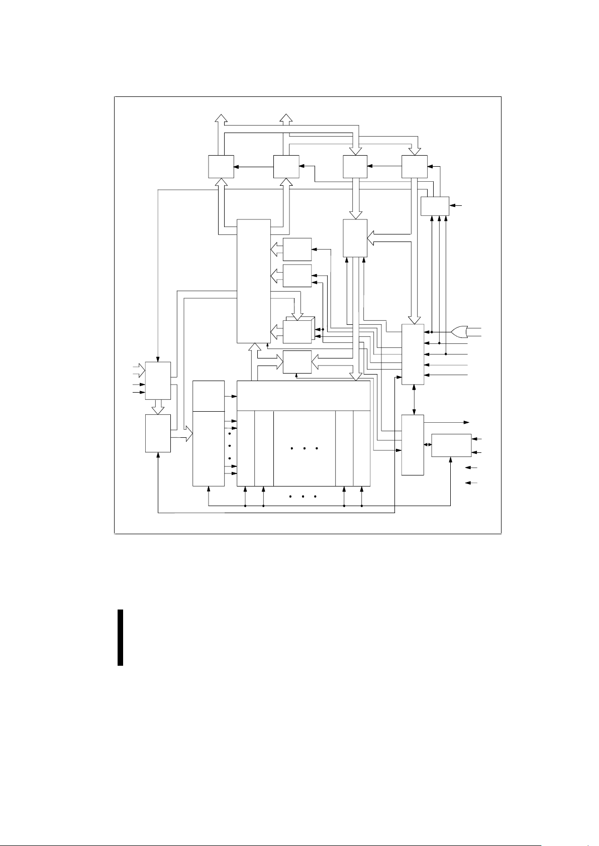
Figure 1. 28F016XD Block Diagram
Architectural Evolution Includes Multiplexed Address Bus,
SmartVoltage Technology, and Extended Registers
Page 8

28F016XD FLASH MEMORY E
8
1
2
3
4
5
6
7
8
9
10
11
12
13
14
15
16
17
18
19
20
21
22
23
24
25
26
27
28
3/5#
GND
NC
A
A
A
A
A
V
RAS#
CAS#
29
30
31
32
33
34
56
55
53
54
52
51
50
49
48
47
46
45
44
43
42
41
40
39
38
37
36
35
NC
NC
GND
V
RP#
NC
NC
NC
NC
GND
NC
NC
A
A
A
A
A
WP#
WE#
OE#
RY/BY#
DQ
DQ
DQ
DQ
GND
DQ
DQ
DQ
DQ
V
GND
DQ
DQ
DQ
DQ
V
DQ
DQ
DQ
DQ
NC
NC
NC
9
8
7
6
5
CC
PP
15
7
14
6
13
5
12
4
CC
11
3
10
2
CC
9
1
8
E28F016XD
56-LEAD TSOP PINOUT
14 mm x 20 mm
TOP VIEW
0
V
CC
4
3
2
1
0
0533_02
Figure 2. 28F016XD 56-Lead TSOP Type I Pinout Configuration
Page 9

E 28F016XD FLASH MEMORY
9
2.1 Lead Descriptions
Symbol Type Name and Function
A0–A
9
INPUT MULTIPLEXED ROW/COLUMN ADDRESSES: Selects a word within
one of thirty-two 32-Kword blocks. Row (upper) addresses are latched on
the falling edge of RAS#, while column (lower) addresses are latched on
the falling edge of CAS#.
DQ0–DQ15INPUT/OUTPUT DATA BUS: Inputs data and commands during CUI write cycles. Outputs
array, identifier or status data (DQ
0-7
) in the appropriate read mode.
Floated when the chip is de-selected or the outputs are disabled.
RAS# INPUT
ROW ADDRESS STROBE: Latches row address information on inputs
A
-
when RAS# transitions low. A subsequent CAS# low transition
initiates 28F016XD read or program operations.
CAS# INPUT
COLUMN ADDRESS STROBE: Latches column address information on
inputs A
-
when CAS# transitions low. When preceded by a RAS# low
transition, CAS# low initiates 28F016XD read or program operations,
along with OE# and WE#. Subsequent CAS# low transitions, with RAS#
held low, enable fast page mode reads/programs
RP# INPUT
RESET/POWER-DOWN: RP# low places the device in a deep powerdown state. All circuits that consume static power, even those circuits
enabled in standby mode, are turned off. When returning from deep
power-down, a recovery time of 300 ns at 5.0V V
is required to allow
these circuits to power-up.
When RP# goes low, the current WSM operation is terminated, and the
device is reset. All Status Registers return to ready (with all status flags
cleared).
Exit from deep power-down places the device in read array mode.
OE# INPUT
OUTPUT ENABLE: Gates device data through the output buffers when
low in combination with RAS# and CAS# low. The outputs float to tri-state
off when OE# is high. OE# can be tied to GND if not controlled by the
system memory controller. RAS# and CAS# high override OE# low. WE#
low also overrides OE# low.
WE# INPUT WRITE ENABLE: Controls access to the CUI, Data Register and Address
Register. WE# is active low and initiates programs in combination with
RAS# and CAS# low. WE# low overrides OE# low. RAS# and CAS# high
override WE# low.
RY/BY# OPEN DRAIN
OUTPUT
READY/BUSY: Indicates status of the internal WSM. When low, it
indicates that the WSM is busy performing an operation. RY/BY# floating
indicates that the WSM is ready for new operations, erase is suspended,
or the device is in deep power-down mode. This output is always active
(i.e., not floated to tri-state off when OE#, RAS# or CAS# are high).
WP# INPUT WRITE PROTECT: Erase blocks can be locked by writing a nonvolatile
lock-bit for each block. When WP# is low, those locked blocks as
reflected by the Block-Lock Status bits (BSR.6), are protected from
inadvertent data programs or erases. When WP# is high, all blocks can
be written or erased regardless of the state of the lock-bits. The WP#
input buffer is disabled when RP# transitions low (deep power-down
mode).
Page 10

28F016XD FLASH MEMORY E
10
2.1 Lead Descriptions (Continued)
Symbol Type Name and Function
3/5# INPUT 3.3/5.0 VOLT SELECT: 3/5# high configures internal circuits for 3.3V
operation. 3/5# low configures internal circuits for 5.0V operation.
NOTE:
Reading the array with 3/5# high in a 5.0V system could damage the
device. Reference the power-up and reset timings (Section 5.9) for 3/5#
switching delay to valid data.
V
SUPPLY PROGRAM/ERASE POWER SUPPLY (12.0V ± 0.6V, 5.0V ± 0.5V): For
erasing memory array blocks or writing words into the flash array. V
=
5.0V ± 0.5V eliminates the need for a 12.0V converter, while connection
to 12.0V ± 0.6V maximizes program/erase performance.
NOTE:
Successful completion of program and erase attempts is inhibited with
V
at or below 1.5V. Program and erase attempts with V
between 1.5V
and 4.5V, between 5.5V and 11.4V, and above 12.6V produce spurious
results and should not be attempted.
V
SUPPLY
DEVICE POWER SUPPLY (3.3V ± 0.3V, 5.0V ± 0.5V):
To switch 3.3V to 5.0V (or vice versa), first ramp V
down to GND, and
then power to the new V
voltage.
Do not leave any power pins floating.
GND SUPPLY
GROUND FOR ALL INTERNAL CIRCUITRY:
Do not leave any ground pins floating.
NC
NO CONNECT:
Lead may be driven or left floating.
Page 11

E 28F016XD FLASH MEMORY
11
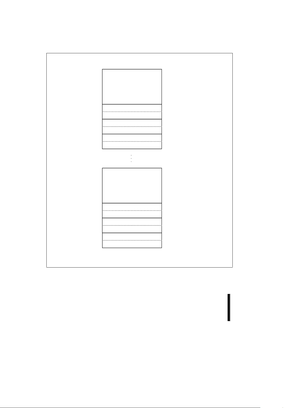
3.0 MEMORY MAPS
32-Kword Block
FFFFF
31
F8000
F7FFF
F0000
EFFFF
E8000
E7FFF
E0000
DFFFF
30
29
28
27
D8000
D7FFF
D0000
CFFFF
C8000
C7FFF
C0000
BFFFF
26
25
24
23
B8000
B7FFF
B0000
A8FFF
A8000
A7FFF
A0000
9FFFF
22
21
20
19
98000
97FFF
90000
8FFFF
88000
87FFF
80000
7FFFF
18
17
16
15
78000
77FFF
70000
6FFFF
68000
67FFF
60000
5FFFF
14
13
12
11
58000
57FFF
50000
4FFFF
48000
47FFF
40000
3FFFF
10
9
8
7
38000
37FFF
30000
2FFFF
28000
27FFF
20000
1FFFF
6
5
4
3
18000
17FFF
10000
0FFFF
08000
07FFF
00000
2
1
0
32-Kword Block
32-Kword Block
32-Kword Block
32-Kword Block
32-Kword Block
32-Kword Block
32-Kword Block
32-Kword Block
32-Kword Block
32-Kword Block
32-Kword Block
32-Kword Block
32-Kword Block
32-Kword Block
32-Kword Block
32-Kword Block
32-Kword Block
32-Kword Block
32-Kword Block
32-Kword Block
32-Kword Block
32-Kword Block
32-Kword Block
32-Kword Block
32-Kword Block
32-Kword Block
32-Kword Block
32-Kword Block
32-Kword Block
32-Kword Block
32-Kword Block
A
[19-0]
0533_03
NOTE:
The upper 10 bits (A
19–10
) reflect 28F016XD addresses A
9–0
, latched by RAS#.
The lower 10 bits (A
9–0
) reflect 28F016XD addresses A
9–0
, latched by CAS#.
Figure 3. 28F016XD Memory Map
Page 12
28F016XD FLASH MEMORY E
12
3.1 Extended Status Registers Memory Map
RESERVED
GSR
RESERVED
BSR0
00002H
00001H
RESERVED
RESERVED
00000H
00003H
RESERVED
07FFFH
RESERVED
GSR
RESERVED
BSR31
F8002H
F8001H
RESERVED
RESERVED
F8000H
F8003H
RESERVED
FFFFFH
A
19-0
0533_04
NOTE:
The upper 10 bits (A
19–10
) reflect 28F016XD addresses A
9–0
, latched by RAS#.
The lower 10 bits (A
9–0
) reflect 28F016XD addresses A
9–0
, latched by CAS#.
Figure 4. Extended Status Registers Memory Map
Page 13

E 28F016XD FLASH MEMORY
13
4.0 BUS OPERATIONS, COMMANDS AND STATUS REGISTER DEFINITIONS
4.1 Bus Operations
Mode Notes RP# RAS# CAS# OE# WE# DQ
0–15
RY/BY#
Row Address Latch 1,2,9 V
IH
↓ V
IH
XX X X
Column Address Latch 1,2,9 V
IH
V
IL
↓ XX X X
Read 1,2,7 V
IH
V
IL
V
IL
V
IL
V
IH
D
OUT
X
Output Disable 1,6,7 V
IH
V
IL
V
IL
V
IH
V
IH
High Z X
Standby 1,6,7 V
IH
V
IH
V
IH
X X High Z X
Deep Power-Down 1,3 V
IL
XXXXHigh Z V
OH
Manufacturer ID 4,8 V
IH
V
IL
V
IL
V
IL
V
IH
0089H V
OH
Device ID 4,8 V
IH
V
IL
V
IL
V
IL
V
IH
66A8H V
OH
Write 1,5,6 V
IH
V
IL
V
IL
XVILD
IN
X
NOTES:
1. X can be V
IH
or V
IL
for address or control pins except for RY/BY#, which is either V
OL
or V
OH
, or High Z or D
OUT
for data
pins depending on whether or not OE# is active.
2. RY/BY# output is open drain. When the WSM is ready, erase is suspended or the device is in deep power-down mode,
RY/BY# will be at V
OH
if it is tied to V
CC
through a resistor. RY/BY# at VOH is independent of OE# while a WSM operation
is in progress.
3. RP# at GND ± 0.2V ensures the lowest deep power-down current.
4. A
0
(latched by CAS#) at VIL provides the Manufacturer ID code. A0 (latched by CAS#) at VIH provides the Device ID code.
All other addresses (row and column) should be set to zero.
5. Commands for erase, data program, or lock-block operations can only be completed successfully when V
PP
= V
PPH1
or
V
PP
= V
PPH2
.
6. While the WSM is running, RY/BY# stays at V
OL
until all operations are complete. RY/BY# goes to VOH when the WSM is
not busy or in erase suspend mode.
7. RY/BY# may be at V
OL
while the WSM is busy performing various operations (for example, a Status Register read during a
program operation).
8. The 28F016XD shares an identical device identifier with the 28F016XS.
9. Row (upper) addresses are latched via inputs A
0-9
on the falling edge of RAS#. Column (lower) addresses are latched via
inputs A
0-9
on the falling edge of CAS#. Row addresses must be latched before column addresses are latched.
Page 14

28F016XD FLASH MEMORY E
14
4.2 28F008SA—Compatible Mode Command Bus Definitions
First Bus Cycle Second Bus Cycle
Command Notes Oper Addr Data
(4)
Oper Addr Data
(4)
Read Array Write X xxFFH Read AA AD
Intelligent Identifier 1 Write X xx90H Read IA ID
Read Compatible Status Register 2 Write X xx70H Read X CSRD
Clear Status Register 3 Write X xx50H
Word Program Write X xx40H Write PA PD
Alternate Word Program Write X xx10H Write PA PD
Block Erase/Confirm Write X xx20H Write BA xxD0H
Erase Suspend/Resume Write X xxB0H Write X xxD0H
ADDRESS DATA
AA = Array Address AD = Array Data
BA = Block Address CSRD = CSR Data
IA = Identifier Address ID = Identifier Data
PA = Program Address PD = Program Data
X = Don’t Care
NOTES:
1. Following the Intelligent Identifier command, two read operations access the manufacturer and device signature codes.
2. The CSR is automatically available after device enters data program, erase, or suspend operations.
3. Clears CSR.3, CSR.4 and CSR.5. Also clears GSR.5 and all BSR.5, BSR.4 and BSR.2 bits. See Status Register
definitions.
4. The upper byte of the data bus (D
8–15
) during command writes is a “Don’t Care.”
Page 15

E 28F016XD FLASH MEMORY
15
4.3 28F016XD—Enhanced Command Bus Definitions
First Bus Cycle Second Bus Cycle
Command Notes Oper Addr Data
(3)
Oper Addr Data
(3)
Read Extended Status Register 1 Write X xx71H Read RA GSRD
BSRD
Lock Block/Confirm Write X xx77H Write BA xxD0H
Upload Status Bits/Confirm 2 Write X xx97H Write X xxD0H
ADDRESS DATA
BA = Block Address AD = Array Data
RA = Extended Register Address BSRD = BSR Data
PA = Program Address GSRD = GSR Data
X = Don’t Care
NOTES:
1. RA can be the GSR address or any BSR address. See Figure 4 for the Extended Status Register memory map.
2. Upon device power-up, all BSR lock-bits come up locked. The Upload Status Bits command must be written to reflect the
actual lock-bit status.
3. The upper byte of the data bus (D
8–15
) during command writes is a “Don’t Care.”
Page 16

28F016XD FLASH MEMORY E
16
4.4 Compatible Status Register
WSMS ESS ES DWS VPPS R R R
76543210
NOTES:
CSR.7 = WRITE STATE MACHINE STATUS
1 = Ready
0 = Busy
RY/BY# output or WSMS bit must be checked to
determine completion of an operation (erase,
erase suspend, or data program) before the
appropriate Status bit (ESS, ES or DWS) is
checked for success.
CSR.6 = ERASE-SUSPEND STATUS
1 = Erase Suspended
0 = Erase In Progress/Completed
CSR.5 = ERASE STATUS
1 = Error In Block Erasure
0 = Successful Block Erase
If DWS and ES are set to “1” during an erase
attempt, an improper command sequence was
entered. Clear the CSR and attempt the
operation again.
CSR.4 = DATA-WRITE STATUS
1 = Error in Data Program
0 = Data Program Successful
CSR.3 = V
STATUS
1 = V
Error Detect, Operation Abort
0 = V
OK
The VPPS bit, unlike an A/D converter, does not
provide continuous indication of V
level. The
WSM interrogates V
PP
’s level only after the Data
Program or Erase command sequences have
been entered, and informs the system if V
PP
has
not been switched on. VPPS is not guaranteed to
report accurate feedback between V
PPL
K
(max)
and V
PPH1
(min), between V
PPH1
(max) and
V
PPH2
(min) and above V
PPH2
(max).
CSR.2–0 = RESERVED FOR FUTURE ENHANCEMENTS
These bits are reserved for future use; mask them out when polling the CSR.
Page 17

E 28F016XD FLASH MEMORY
17
4.5 Global Status Register
WSMS OSS DOS R R R R R
76543210
NOTES:
GSR.7 = WRITE STATE MACHINE STATUS
1 = Ready
0 = Busy
RY/BY# output or WSMS bit must be checked to
determine completion of an operation (block lock,
suspend, Upload Status Bits, erase or data
program) before the appropriate Status bit (OSS
or DOS) is checked for success.
GSR.6 = OPERATION SUSPEND STATUS
1 = Operation Suspended
0 = Operation in Progress/Completed
GSR.5 = DEVICE OPERATION STATUS
1 = Operation Unsuccessful
0 = Operation Successful or Currently
Running
GSR.4–0 = RESERVED FOR FUTURE ENHANCEMENTS
These bits are reserved for future use; mask them out when polling the GSR.
Page 18

28F016XD FLASH MEMORY E
18
4.6 Block Status Register
BS BLS BOS R R VPPS VPPL R
76543210
NOTES:
BSR.7 = BLOCK STATUS
1 = Ready
0 = Busy
RY/BY# output or BS bit must be checked to
determine completion of an operation (block lock,
suspend, erase or data program) before the
appropriate Status bits (BOS, BLS) is checked
for success.
BSR.6 = BLOCK LOCK STATUS
1 = Block Unlocked for Program/Erase
0 = Block Locked for Program/Erase
BSR.5 = BLOCK OPERATION STATUS
1 = Operation Unsuccessful
0 = Operation Successful or
Currently Running
BSR.2 = V
STATUS
1 = V
Error Detect, Operation Abort
0 = V
OK
BSR.1 = V
LEVEL
1 = V
Detected at 5.0V ± 10%
0 = V
Detected at 12.0V ± 5%
BSR.1 is not guaranteed to report accurate
feedback between the V
and V
voltage
ranges. Programs and erases with V
between
V
(max) and V
(min), between
V
(max) and V
(min), and above
V
(max) produce spurious results and should
not be attempted.
BSR.1 was a RESERVED bit on the 28F016SA.
BSR.4,3,0 = RESERVED FOR FUTURE ENHANCEMENTS
These bits are reserved for future use; mask them out when polling the BSRs.
Page 19

E 28F016XD FLASH MEMORY
19
5.0 ELECTRICAL SPECIFICATIONS
5.1 Absolute Maximum Ratings*
Temperature Under Bias ....................0°C to +80°C
Storage Temperature ...................–65°C to +125°C
NOTICE: This is a production datasheet. The
specifications are subject to change without notice. Verify
with your local Intel Sales office that you have the latest
datasheet before finalizing a design.
*WARNING: Stressing the device beyond the “Absolute
Maximum Ratings” may cause permanent damage.
These are stress ratings only. Operation beyond the
“Operating Conditions” is not recommended and
extended exposure beyond the "Operating Conditions"
may affect device reliability.
VCC = 3.3V ± 0.3V Systems
Sym Parameter Notes Min Max Units Test Conditions
T
A
Operating Temperature, Commercial 1 0 70 °C Ambient Temperature
VCCVCC with Respect to GND 2 –0.2 7.0 V
VPPV
PP
Supply Voltage with Respect to GND 2,3 –0.2 14.0 V
V Voltage on any Pin (except VCC,VPP) with
Respect to GND
2,5 –0.5 V
CC
+
0.5
V
I Current into any Non-Supply Pin 5 ± 30 mA
I
OUT
Output Short Circuit Current 4 100 mA
V
CC
= 5.0V ± 0.5V Systems
Sym Parameter Notes Min Max Units Test Conditions
T
A
Operating Temperature, Commercial 1 0 70 °C Ambient Temperature
VCCVCC with Respect to GND 2 –0.2 7.0 V
VPPVPP Supply Voltage with Respect to GND 2,3 –0.2 14.0 V
V Voltage on any Pin (except VCC,VPP) with
Respect to GND
2,5 –2.0 7.0 V
I Current into any Non-Supply Pin 5 ± 30 mA
I
OUT
Output Short Circuit Current 4 100 mA
NOTES:
1. Operating temperature is for commercial product defined by this specification.
2. Minimum DC voltage is –0.5V on input/output pins. During transitions, this level may undershoot to –2.0V for periods
<20 ns. Maximum DC voltage on input/output pins is V
CC
+ 0.5V which, during transitions, may overshoot to VCC + 2.0V for
periods <20 ns.
3. Maximum DC voltage on V
PP
may overshoot to +14.0V for periods <20 ns.
4. Output shorted for no more than one second. No more than one output shorted at a time.
5. This specification also applies to pins marked “NC.”
Page 20

28F016XD FLASH MEMORY E
20
5.2 Capacitance
For a 3.3V ± 0.3V System:
Sym Parameter Notes Typ Max Units Test Conditions
C
IN
Capacitance Looking into an
Address/Control Pin
168pFT
A
= +25°C, f = 1.0 MHz
C
OUT
Capacitance Looking into an
Output Pin
1 8 12 pF T
A
= +25°C, f = 1.0 MHz
C
LOAD
Load Capacitance Driven by
Outputs for Timing Specifications
1,2 50 pF
For 5.0V ± 0.5V System:
Sym Parameter Notes Typ Max Units Test Conditions
C
IN
Capacitance Looking into an
Address/Control Pin
168pFTA = +25°C, f = 1.0 MHz
C
OUT
Capacitance Looking into an
Output Pin
1 8 12 pF TA = +25°C, f = 1.0 MHz
C
LOAD
Load Capacitance Driven by
Outputs for Timing Specifications
1,2 100 pF
NOTE:
1. Sampled, not 100% tested.
2. To obtain iBIS models for the 28F016XD, please contact your local Intel/Distribution Sales Office.
Page 21

E 28F016XD FLASH MEMORY
21
5.3 Transient Input/Output Reference Waveforms
TEST POINTS
INPUT OUTPUT
2.0
0.8 0.8
2.0
2.4
0.45
0533_05
AC test inputs are driven at VOH (2.4 VTTL) for a Logic “1” and VOL (0.45 VTTL) for a Logic “0.” Input timing begins at V
IH
(2.0 VTTL) and VIL (0.8 VTTL). Output timing ends at VIH and VIL. Input rise and fall times (10% to 90%) <10 ns.
Figure 5. Transient Input/Output Reference Waveform for VCC = 5.0V ± 0.5V
(1)
TEST POINTSINPUT
OUTPUT
1.5
3.0
0.0
1.5
0533_06
AC test inputs are driven at 3.0V for a Logic “1” and 0.0V for a Logic “0.” Input timing begins, and output timing ends, at 1.5V.
Input rise and fall times (10% to 90%) <10 ns.
Figure 6. Transient Input/Output Reference Waveform for VCC = 3.3V ± 0.3V
(2)
NOTES:
1. Testing characteristics for 28F016XD-85.
2. Testing characteristics for 28F016XD-95.
Page 22

28F016XD FLASH MEMORY E
22
5.4 DC Characteristics
VCC = 3.3V ± 0.3V, TA = 0°C to +70°C
3/5# = Pin Set High for 3.3V Operations
Sym Parameter Notes Min Typ Max Unit Test Condition
ICC1VCC Word Read
Current
1,4,5 50 70 mA VCC = VCC Max
RAS#, CAS# = V
IL
RAS#, CAS#, Addr. Cycling @
t
RC
= min
I
OUT
= 0 mA
Inputs = TTL or CMOS
ICC2VCC Standby Current 1,5 1 4 mA VCC = VCC Max
RAS#, CAS#, RP# = V
IH
WP#, 3/5# = VIL or V
IH
ICC3VCC RAS#-Only
Refresh Current
1,5 50 80 mA VCC = VCC Max
CAS# = V
IH
RAS# = V
IL
RAS#, Addr. Cycling @
t
RC
= min
Inputs = TTL or CMOS
ICC4VCC Fast Page Mode
Word Read Current
1,4,5 40 70 mA VCC = VCC Max
RAS#, CAS# = V
IL
CAS#, Addr. Cycling @
t
PC
= min
I
OUT
= 0 mA
Inputs = V
IL
or V
IH
ICC5VCC Standby Current 1,5 70 130 µA VCC = VCC Max
RAS# CAS# RP# = V
CC
± 0.2V
WP#, 3/5# = V
CC
± 0.2V or
GND ± 0.2V
ICC6VCC CAS#-before-
RAS# Refresh Current
1,5 40 15 mA VCC = VCC Max
CAS#, RAS# = V
IL
CAS#, RAS#, Addr. Cycling @
t
RC
= min
Inputs = TTL or CMOS
ICC7VCC Standby Current
(Self Refresh Mode)
1,5 40 10 mA VCC = VCC Max
RAS#, CAS# = V
IL
I
OUT
= 0 mA
Inputs = V
IL
or V
IH
I
LI
Input Load Current 1 ± 1 µA V
CC
= V
CC
Max
V
IN
= V
CC
or GND
I
LO
Output Leakage
Current
1 ± 10 µA V
CC
= V
CC
Max
V
OUT
= V
CC
or GND
I
CCDVCC
Deep Power-
Down Current
1 2 10 µA RP# = GND ± 0.2V
Page 23

E 28F016XD FLASH MEMORY
23
5.4 DC Characteristics (Continued)
V
CC
= 3.3V ± 0.3V, TA = 0°C to +70°C
3/5# = Pin Set High for 3.3V Operations
Sym Parameter Notes Min Typ Max Unit Test Condition
I
CCWVCC
Word Program
Current
1,6 8 12 mA VPP = 12.0V ± 5%
Program in Progress
817mAVPP = 5.0V ± 10%
Program in Progress
I
CCE
VCC Block Erase
Current
1,6 6 12 mA VPP = 12.0V ± 5%
Block Erase in Progress
917mAVPP = 5.0V ± 10%
Block Erase in Progress
I
CCESVCC
Erase Suspend
Current
1,2 1 4 mA RAS#, CAS# = V
IH
Block Erase Suspended
I
PPS
VPP Standby/Read 1 ± 1 ± 10 µA VPP ≤ V
CC
Current 30 200 µA VPP > V
CC
I
PPD
VPP Deep PowerDown Current
1 0.2 5 µA RP# = GND ± 0.2V
I
PPW
V
Word Program
Current
1,6 10 15 mA VPP = 12.0V ± 5%
Program in Progress
15 25 mA VPP = 5.0V ± 10%
Program in Progress
I
PPE
VPP Block Erase
Current
1,6 4 10 mA VPP = 12.0V ± 5%
Block Erase in Progress
14 20 mA VPP = 5.0V ± 10%
Block Erase in Progress
I
PPESVPP
Erase Suspend
Current
1 30 200 µA Block Erase Suspended
V
IL
Input Low Voltage 6 -0.3 0.8 V
V
IH
Input High Voltage 6 2.0 V
+
0.3
V
V
OL
Output Low Voltage 6 0.4 V V
CC
= V
CC
Min
I
OL
= 4.0 mA
V
OH1
Output High Voltage 6 2.4 V VCC = VCC Min
I
OH
= –2.0 mA
V
OH2
6VCC-
0.2
VV
CC
= V
CC
Min
I
OH
= –100 µA
V
PPL
K
V
Erase/Program
Lock Voltage
3,6 0.0 1.5 V
V
PPH
1VPP during Program/
Erase Operations
3 4.5 5.0 5.5 V
V
PPH
2VPP during Program/
Erase Operations
3 11.4 12.0 12.6 V
V
LKO
V
Erase/Program
Lock Voltage
2.0 V
Page 24

28F016XD FLASH MEMORY E
24
NOTES:
1. All currents are in RMS unless otherwise noted. Typical values at V
CC
= 3.3V, VPP = 12.0V or 5.0V, T = +25°C.
2.
I
CCES
is specified with the device de-selected. If the device is read while in erase suspend mode, current draw is the sum of
I
CCES
and I
CC1/ICC4
.
3. Block erases, word programs and lock block operations are inhibited when V
PP
= V
PPLK
and not guaranteed in the ranges
between V
PPLK(max)
and V
PPH1(min)
, between V
PPH1(max) and VPPH2(min) , and above VPPH2(max)
.
4. Automatic Power Saving (APS) reduces I
CC1
and I
CC4
to 3.0 mA typical in static operation.
5. CMOS inputs are either V
CC
± 0.2V or GND ± 0.2V. TTL inputs are either VIL or VIH.
6. Sampled, but not 100% tested. Guaranteed by design.
Page 25

E 28F016XD FLASH MEMORY
25
5.5 DC Characteristics
VCC = 5.0V ± 0.5V, TA = 0°C to +70°C
3/5# = Pin Set Low for 5.0V Operations
Sym Parameter Notes Min Typ Max Unit Test Condition
ICC1V
Word Read
Current
1,4,5 90 120 mA VCC = VCC Max
RAS#, CAS# = V
IL
RAS#, CAS#, Addr. Cycling @
t
RC
= min
I
OUT
= 0 mA
Inputs = TTL or CMOS
ICC2VCC Standby Current 1,5 2 4 mA VCC = VCC Max
RAS#, CAS#, RP# = V
IH
WP#, 3/5# = VIL or V
IH
ICC3VCC RAS#-Only
Refresh Current
1,5 90 145 mA VCC = VCC Max
CAS# = V
IH
RAS# = V
IL
RAS#, Addr. Cycling @
t
RC
= min
Inputs = TTL or CMOS
ICC4VCC Fast Page Mode
Word Read Current
1,4,5 80 130 mA VCC = VCC Max
RAS#, CAS# = V
IL
CAS#, Addr. Cycling @
t
PC
= min
I
OUT
= 0 mA
Inputs = V
IL
or V
IH
ICC5VCC Standby Current 1,5 70 130 µA VCC = VCC Max
RAS#,CAS#,RP# = V
CC
± 0.2V
WP#, 3/5# = V
CC
± 0.2V or
GND ± 0.2V
ICC6VCC CAS#-before-
RAS# Refresh Current
1,5 50 15 mA VCC = VCC Max
CAS#, RAS# = V
IL
CAS#, RAS#, Addr. Cycling @
t
RC
= min
Inputs = TTL or CMOS
ICC7VCC Standby Current
(Self Refresh Mode)
1,5 50 10 mA VCC = VCC Max
RAS#, CAS# = V
IL
I
OUT
= 0 mA
Inputs = V
IL
or V
IH
I
LI
Input Load Current 1 ± 1 µA V
CC
= V
CC
Max
V
IN
= V
CC
or GND
I
LO
Output Leakage
Current
1 ± 10 µA V
CC
= V
CC
Max
V
OUT
= V
CC
or GND
I
CCDVCC
Deep Power-Down
Current
1 2 10 µA RP# = GND ± 0.2V
Page 26

28F016XD FLASH MEMORY E
26
5.5 DC Characteristics (Continued)
V
CC
= 5.0V ± 0.5V, TA = 0°C to +70°C
3/5# = Pin Set Low for 5.0V Operations
Sym Parameter Notes Min Typ Max Unit Test Condition
I
CCW
V
Word Program
Current
1,6 25 35 mA VPP = 12.0V ± 5%
Word Program in Progress
25 40 mA VPP = 5.0V ± 10%
Word Program in Progress
I
CCEVCC
Block Erase Current 1,6 18 25 mA VPP = 12.0V ± 5%
Block Erase in Progress
20 30 mA VPP = 5.0V ± 10%
Block Erase in Progress
I
CCESVCC
Erase Suspend
Current
1,2 2 4 mA RAS#, CAS# = V
IH
Block Erase Suspended
I
PPSVPP
Standby/Read 1 ± 1 ± 10 µA VPP ≤ V
CC
Current 30 200 µA VPP > V
CC
I
PPDVPP
Deep Power-Down
Current
1 0.2 5 µA RP# = GND ± 0.2V
I
PPW
V
Word Program
Current
1,6 7 12 mA VPP = 12.0V ± 5%
Word Program in Progress
17 22 mA VPP = 5.0V ± 10%
Word Program in Progress
I
PPEVPP
Block Erase Current 1,6 5 10 mA VPP = 12.0V ± 5%
Block Erase in Progress
16 20 mA VPP = 5.0V ± 10%
Block Erase in Progress
I
PPESVPP
Erase Susp.Current 1 30 200 µA Block Erase Suspended
V
IL
Input Low Voltage 6 –0.5 0.8 V
V
IH
Input High Voltage 6 2.0 V
+
0.5
V
V
OL
Output Low Voltage 6 0.45 V V
CC
= V
CC
Min
I
OL
= 5.8 mA
V
OH1
Output High Voltage 6 0.85
V
CC
VVCC = VCC Min
I
OH
= –2.5 mA
V
OH2
6V
–
0.4
VV
CC
= V
CC
Min
I
OH
= –100 µA
V
PPL
K
VPP Erase/Program Lock
Voltage
3,6 0.0 1.5 V
V
PPH
1VPP during Program/Erase
Operations
3 4.5 5.0 5.5 V
V
PPH
2VPP during Program/Erase
Operations
3 11.4 12.0 12.6 V
V
LKOVCC
Erase/Program Lock
Voltage
2.0 V
Page 27

E 28F016XD FLASH MEMORY
27
NOTES:
1. All currents are in RMS unless otherwise noted. Typical values at V
CC
= 5.0V, VPP = 12.0V or 5.0V, T = +25°C. These
currents are specified for a CMOS rise/fall time (10% to 90%) of <5 ns and a TTL rise/fall time of <10 ns.
2.
I
CCES
is specified with the device de-selected. If the device is read while in Erase Suspend mode, current draw is the sum
of
I
CCES
and I
CC1/ICC4
.
3. Block erases, word programs and lock block operations are inhibited when V
PP
= V
PPLK
and not guaranteed in the ranges
between V
PPLK(max)
and V
PPH1(min)
, between V
PPH1(max) and VPPH2(min), and above VPPH2(max)
.
4. Automatic Power Saving (APS) reduces I
CC1
and I
CC4
to 1 mA typical in static operation.
5. CMOS inputs are either V
CC
± 0.2V or GND ± 0.2V. TTL inputs are either VIL or VIH.
6. Sampled, not 100% tested. Guaranteed by design.
Page 28

28F016XD FLASH MEMORY E
28
5.6 AC Characteristics
(11)
V
CC
= 3.3V ± 0.3V, TA = 0°C to +70°C
Read, Program, Read-Modify-Program and Refresh Cycles (Common Parameters)
Versions 28F016XD-95 Units
Sym Parameter Notes Min Max
t
RP
RAS# precharge time 10 ns
t
CP
CAS# precharge time 15 ns
t
ASR
Row address set-up time 9 0 ns
t
RAH
Row address hold time 9 15 ns
t
ASC
Column address set-up time 9 0 ns
t
CAH
Column address hold time 9 20 ns
t
AR
Column address hold time referenced to RAS# 3,9 35 ns
t
RAD
RAS# to column address delay time 8,9 15 15 ns
t
CRP
CAS# to RAS# precharge time 10 ns
t
OED
OE# to data delay 10 30 ns
t
DZO
OE# delay time from data-in 10 0 ns
t
DZC
CAS# delay time from data-in 10 0 ns
t
T
Transition time (rise and fall) 10 2 4 ns
Read Cycle
Versions 28F016XD-95 Units
Sym Parameter Notes Min Max
t
RC(R)
Random read cycle time 105 ns
t
RAS(R)
RAS# pulse width (reads) 95
∞
ns
t
CAS(R)
CAS# pulse width (reads) 45
∞
ns
t
RCD(R)
RAS# to CAS# delay time (reads) 1 15 50 ns
t
RSH(R)
RAS# hold time (reads) 30 ns
t
CSH(R)
CAS# hold time (reads) 95 ns
t
RAC
Access time from RAS# 1,8 95 ns
t
CAC
Access time from CAS# 1,2 40 ns
t
AA
Access time from column address 8 75 ns
t
OEA
OE# access time 40 ns
Page 29

E 28F016XD FLASH MEMORY
29
Read Cycle (Continued)
Versions 28F016XD-95 Units
Sym Parameter Notes Min Max
t
ROH
RAS# hold time referenced to OE# 40 ns
t
RCS
Read command setup time 5 ns
t
RCH
Read command hold time referenced to CAS# 6,10 0 ns
t
RRH
Read command hold time referenced to RAS# 6,10 0 ns
t
RAL
Column address to RAS# lead time 9 15 ns
t
CAL
Column address to CAS# lead time 9 75 ns
t
CLZ
CAS# to output in Low-Z 0 ns
t
OH
Output data hold time 0 ns
t
OHO
Output data hold time from OE# 0 ns
t
OFF
Output buffer turn-off delay 4 30 ns
t
OEZ
Output buffer turn off delay time from OE# 30 ns
t
CDD
CAS# to data-in delay time 30 ns
Write Cycle
Versions 28F016XD-95 Units
Sym Parameter Notes Min Max
t
RC(W)
Random write cycle time 90 ns
t
RAS(W)
RAS# pulse width (writes) 80
∞
ns
t
CAS(W)
CAS# pulse width (writes) 65
∞
ns
t
RCD(W)
RAS# to CAS# delay time (writes) 1 15 15 ns
t
RSH(W)
RAS# hold time (writes) 65 ns
t
CSH(W)
CAS# hold time (writes) 80 ns
t
WCS
Write command set-up time 5 0 ns
t
WCH
Write command hold time 15 ns
t
WCR
Write command hold time referenced to RAS# 3 30 ns
t
WP
Write command pulse width 15 ns
t
RWL
Write command to RAS# lead time 65 ns
t
CWL
Write command to CAS# lead time 65 ns
t
DS
Data-in set-up time 7,9 0 ns
t
DH
Data-in hold time 7,9 15 ns
t
DHR
Data-in hold time referenced to RAS# 3,9 30 ns
Page 30

28F016XD FLASH MEMORY E
30
Read-Modify-Write Cycle
Versions 28F016XD-95 Units
Sym Parameter Notes Min Max
t
RWC
Read-modify-write cycle time 10 200 ns
t
RWD
RAS# to WE# delay time 5,10 125 ns
t
CWD
CAS# to WE# delay time 5,10 75 ns
t
AWD
Column address to WE# delay time 5,9,10 105 ns
t
OEH
OE# command hold time 10 15 ns
Fast Page Mode Cycle
Versions 28F016XD-95 Units
Sym Parameter Notes Min Max
t
PC(R)
Fast page mode cycle time (reads) 75 ns
t
PC(W)
Fast page mode cycle time (writes) 80 ns
t
RASP(R)
RAS# pulse width (reads) 95
∞
ns
t
RASP(W)
RAS# pulse width (writes) 80
∞
ns
t
CPA
Access time from CAS# precharge 85 ns
t
CPW
WE# delay time from CAS# precharge 10 0 ns
t
CPRH(R)
RAS# hold time from CAS# precharge (reads) 75 ns
t
CPRH(W)
RAS# hold time from CAS# precharge (writes) 80 ns
Fast Page Mode Read-Modify-Write Cycle
Versions 28F016XD-95 Units
Sym Parameter Notes Min Max
t
PRWC
Fast page mode read-modify-write cycle time 10 170 ns
Page 31

E 28F016XD FLASH MEMORY
31
Refresh Cycle
Versions 28F016XD-95 Units
Sym Parameter Notes Min Max
t
CSR
CAS# set-up time (CAS#-before-RAS# refresh) 10 10 ns
t
CHR
CAS# hold time (CAS#-before-RAS# refresh) 10 10 ns
t
WRP
WE# setup time (CAS#-before-RAS# refresh) 10 10 ns
t
WRH
WE# hold time (CAS#-before-RAS# refresh) 10 10 ns
t
RPC
RAS# precharge to CAS# hold time 10 10 ns
t
RASS
RAS# pulse width (self-refresh mode) 10 0 ns
t
RPS
RAS# precharge time (self-refresh mode) 10 10 ns
t
CPN
CAS# precharge time (self-refresh mode) 10 10 ns
t
CHS
CAS# hold time (self-refresh mode) 10 0 ns
Refresh
Versions 28F016XD-95 Units
Sym Parameter Notes Min Max
t
REF
Refresh period 10
∞
ms
Misc. Specifications
Versions 28F016XD-95 Units
Parameter Notes Min Max
RP# high to RAS# going low 10 480 ns
RP# set-up to WE# going low 10 480 ns
VPP set-up to CAS# high at end of write cycle 10 100 ns
WE# high to RY/BY# going low 10 100 ns
RP# hold from valid status register data and RY/BY# high 10 0 ns
VPP hold from valid status register data and RY/BY# high 10 0 ns
Page 32

28F016XD FLASH MEMORY E
32
NOTES:
1. Operation within the t
RCD(max)
limit insures that t
RAC(max)
can be met. t
RCD(max)
is specified as a reference point.
2. Assumes that t
RCD
≥t
RCD(max)
.
3. t
AR
, t
WCR
, t
DHR
are referenced to t
RAD(max)
.
4. t
OFF(max)
defines the time at which the output achieves the open circuit condition and is not referenced to VOH or VOL.
5. t
WCS
, t
RWD
, t
CWD
and t
AWD
are non restrictive operating parameters. They are included in the datasheet as electrical
characteristics only. If t
WCS
≥t
WCS(min)
the cycle is an early write cycle and the data output will remain high impedance for
the duration of the cycle. If t
CWD
≥t
CWD(min)
, t
RWD
≥t
RWD(min)
, t
AWD
≥t
AWD(min)
, then the cycle is a read-write cycle and the
data output will contain the data read from the selected address. If neither of the above conditions are satisfied, the
condition of the data out is indeterminate.
6. Either t
RCH
or t
RRH
must be satisfied for a read cycle.
7. These parameters are referenced to the CAS# leading edge in early write cycles and to the WE# leading edge in readwrite cycles.
8. Operation within the t
RAD(max)
limit ensures that t
RAC(max)
can be met, t
RAD(max)
is specified as a reference point only. If t
RAD
is greater than the specified t
RAD(max)
limit, then the access time is controlled by tAA.
9. Refer to command definition tables for valid address and data values.
10. Sampled, but not 100% tested. Guaranteed by design.
11. See AC Input/Output Reference Waveforms for timing measurements.
Page 33

E 28F016XD FLASH MEMORY
33
5.7 AC Characteristics
(11)
V
CC
= 5.0V ± 0.5V, TA = 0°C to +70°C
Read, Write, Read-Modify-Write and Refresh Cycles (Common Parameters)
Versions 28F016XD-85 Units
Sym Parameter Notes Min Max
t
RP
RAS# precharge time 10 ns
t
CP
CAS# precharge time 15 ns
t
ASR
Row address set-up time 9 0 ns
t
RAH
Row address hold time 9 15 ns
t
ASC
Column address set-up time 9 0 ns
t
CAH
Column address hold time 9 20 ns
t
AR
Column address hold time referenced to RAS# 3,9 35 ns
t
RAD
RAS# to column address delay time 8,9 15 15 ns
t
CRP
CAS# to RAS# precharge time 10 ns
t
OED
OE# to data delay 10 30 ns
t
DZO
OE# delay time from data-in 10 0 ns
t
DZC
CAS# delay time from data-in 10 0 ns
t
T
Transition time (rise and fall) 10 2 4 ns
Page 34

28F016XD FLASH MEMORY E
34
Read Cycle
Versions 28F016XD-85 Units
Sym Parameter Notes Min Max
t
RC(R)
Random read cycle time 95 ns
t
RAS(R)
RAS# pulse width (reads) 85
∞
ns
t
CAS(R)
CAS# pulse width (reads) 35
∞
ns
t
RCD(R)
RAS# to CAS# delay time (reads) 1 15 50 ns
t
RSH(R)
RAS# hold time (reads) 30 ns
t
CSH(R)
CAS# hold time (reads) 85 ns
t
RAC
Access time from RAS# 1,8 85 ns
t
CAC
Access time from CAS# 1,2 35 ns
t
AA
Access time from column address 8 65 ns
t
OEA
OE# access time 35 ns
t
ROH
RAS# hold time referenced to OE# 35 ns
t
RCS
Read command setup time 5 ns
t
RCH
Read command hold time referenced to CAS# 6,10 0 ns
t
RRH
Read command hold time referenced to RAS# 6,10 0 ns
t
RAL
Column address to RAS# lead time 9 15 ns
t
CAL
Column address to CAS# lead time 9 65 ns
t
CLZ
CAS# to output in Low-Z 10 0 ns
t
OH
Output data hold time 10 0 ns
t
OHO
Output data hold time from OE# 10 0 ns
t
OFF
Output buffer turn-off delay 4,10 30 ns
t
OEZ
Output buffer turn off delay time from OE# 10 30 ns
t
CDD
CAS# to data-in delay time 10 30 ns
Page 35

E 28F016XD FLASH MEMORY
35
Write Cycle
Versions 28F016XD-85 Units
Sym Parameter Notes Min Max
t
RC(W)
Random write cycle time 75 ns
t
RAS(W)
RAS# pulse width (writes) 65
∞
ns
t
CAS(W)
CAS# pulse width (writes) 50
∞
ns
t
RCD(W)
RAS# to CAS# delay time (writes) 1 15 15 ns
t
RSH(W)
RAS# hold time (writes) 50 ns
t
CSH(W)
CAS# hold time (writes) 65 ns
t
WCS
Write command set-up time 5 0 ns
t
WCH
Write command hold time 15 ns
t
WCR
Write command hold time referenced to RAS# 3 30 ns
t
WP
Write command pulse width 15 ns
t
RWL
Write command to RAS# lead time 50 ns
t
CWL
Write command to CAS# lead time 50 ns
t
DS
Data-in set-up time 7,9 0 ns
t
DH
Data-in hold time 7,9 15 ns
t
DHR
Data-in hold time referenced to RAS# 3,9 30 ns
Read-Modify-Write Cycle
Versions 28F016XD-85 Units
Sym Parameter Notes Min Max
t
RWC
Read-modify-write cycle time 10 175 ns
t
RWD
RAS# to WE# delay time 5,10 115 ns
t
CWD
CAS# to WE# delay time 5,10 65 ns
t
AWD
Column address to WE# delay time 5,9,10 100 ns
t
OEH
OE# command hold time 10 15 ns
Fast Page Mode Cycle
Versions 28F016XD-85 Units
Sym Parameter Notes Min Max
t
PC(R)
Fast page mode cycle time (reads) 65 ns
t
PC(W)
Fast page mode cycle time (writes) 65 ns
Page 36

28F016XD FLASH MEMORY E
36
Fast Page Mode Cycle Continued
Versions 28F016XD-85 Units
Sym Parameter Notes Min Max
t
RASP(R)
RAS# pulse width (reads) 85
∞
ns
t
RASP(W)
RAS# pulse width (writes) 65
∞
ns
t
CPA
Access time from CAS# precharge 70 ns
t
CPW
WE# delay time from CAS# precharge 10 0 ns
t
CPRH(R)
RAS# hold time from CAS# precharge (reads) 65 ns
t
CPRH(W)
RAS# hold time from CAS# precharge (writes) 65 ns
Fast Page Mode Read-Modify-Write Cycle
Versions 28F016XD-85 Units
Sym Parameter Notes Min Max
t
PRWC
Fast page mode read-modify-write cycle time 10 145 ns
Refresh Cycle
Versions 28F016XD-85 Units
Sym Parameter Notes Min Max
t
CSR
CAS# set-up time (CAS#-before-RAS# refresh) 10 10 ns
t
CHR
CAS# hold time (CAS#-before-RAS# refresh) 10 10 ns
t
WRP
WE# setup time (CAS#-before-RAS# refresh) 10 10 ns
t
WRH
WE# hold time (CAS#-before-RAS# refresh) 10 10 ns
t
RPC
RAS# precharge to CAS# hold time 10 10 ns
t
RASS
RAS# pulse width (self-refresh mode) 10 0 ns
t
RPS
RAS# precharge time (self-refresh mode) 10 10 ns
t
CPN
CAS# precharge time (self-refresh mode) 10 10 ns
t
CHS
CAS# hold time (self-refresh mode) 10 0 ns
Refresh
Versions 28F016XD-85 Units
Sym Parameter Notes Min Max
t
REF
Refresh period 10
∞
ms
Page 37

E 28F016XD FLASH MEMORY
37
Misc. Specifications
Versions 28F016XD-85 Units
Parameter Notes Min Max
RP# high to RAS# going low 10 300 ns
RP# set-up to WE# going low 10 300 ns
VPP set-up to CAS# high at end of write cycle 10 100 ns
WE# high to RY/BY# going low 10 100 ns
RP# hold from valid status register data and RY/BY# high 10 0 ns
VPP hold from valid status register data and RY/BY# high 10 0 ns
NOTES:
1. Operation within the t
RCD(max)
limit insures that t
RAC(max)
can be met. t
RCD(max)
is specified as a reference point.
2. Assumes that t
RCD≥tRCD(max)
.
3. t
AR
, t
WCR
, t
DHR
are referenced to t
RAD(max)
.
4. t
OFF(max)
defines the time at which the output achieves the open circuit condition and is not referenced to VOH or VOL.
5. t
WCS
, t
RWD
, t
CWD
and t
AWD
are non restrictive operating parameters. They are included in the datasheet as electrical
characteristics only. If t
WCS≥tWCS(min)
the cycle is an early write cycle and the data output will remain high impedance for
the duration of the cycle. If t
CWD≥tCWD(min)
, t
RWD≥tRWD(min)
, t
AWD≥tAWD(min)
, then the cycle is a read-write cycle and the data
output will contain the data read from the selected address. If neither of the above conditions are satisfied, the condition of
the data out is indeterminate.
6. Either t
RCH
or t
RRH
must be satisfied for a read cycle.
7. These parameters are referenced to the CAS# leading edge in early write cycles and to the WE# leading edge in readwrite cycles.
8. Operation within the t
RAD(max)
limit ensures that t
RAC(max)
can be met, t
RAD(max)
is specified as a reference point only. If t
RAD
is greater than the specified t
RAD(max)
limit, then the access time is controlled by tAA.
9. Refer to command definition tables for valid address and data values.
10. Sampled, but not 100% tested. Guaranteed by design.
11. See AC Input/Output Reference Waveforms for timing measurements.
Page 38

28F016XD FLASH MEMORY E
38
5.8 AC Waveforms
: Don’t Care
t
RC
t
RAS
t
RP
t
CSH
t
RCD
t
CAS
t
RSH
ColumnRow
t
T
RAS#
CAS#
Address
WE#
t
RCS
Din
OE#
Dout
Dout
OPEN
t
OED
t
CDD
t
RCH
t
RRH
t
ASC
t
RAH
t
ASR
t
CAH
t
RAC
t
AA
t
CAC
t
OH
t
OFF
t
OHO
t
OEZ
t
OEA
t
DZO
t
DZC
t
CAL
t
RAL
t
RAD
t
CRP
0533-07
Figure 7. AC Waveforms for Read Operations
Page 39

E 28F016XD FLASH MEMORY
39
t
RC
t
RAS
t
RP
t
CSH
t
RCD
t
CAS
t
RSH
t
CRP
t
CAH
t
ASC
t
RAH
t
ASR
t
WCS
t
WCH
t
DS
t
DH
Column
Row
t
T
Din
OPEN
RAS#
CAS#
Address
WE#
Din
Dout
OE# : Don’t Care
: Don’t Care
t
WCS
>
_
t
WCS (min)
0528_08
Figure 8. AC Waveforms for Early Write Operations
Page 40

28F016XD FLASH MEMORY E
40
: Don’t Care
t
RC
t
RAS
t
RP
t
CSH
t
RCD
t
CAS
t
RSH
t
CRP
t
CAH
t
ASC
t
RAH
t
ASR
Column
Row
t
T
RAS#
CAS#
Address
WE#
Din
Din
OPEN
OE#
Invalid
Dout
t
CWL
t
RWL
t
WP
t
QEH
t
DS
t
DH
t
QED
t
CLZ
t
QEZ
t
DZC
t
DZO
Dout
t
RCS
0533_09
Figure 9. AC Waveforms for Delayed Write Operations
Page 41

E 28F016XD FLASH MEMORY
41
: Don’t Care
t
RWC
t
RAS
t
RP
t
RCD
t
CAS
Column
Row
t
T
RAS#
CAS#
Address
WE#
t
RCS
Din
Din
OPEN
OE#
DoutDout
t
ASR
t
RAH
t
ASC
t
CAH
t
CRP
t
RAD
t
CWD
t
AWD
t
RWD
t
CWL
t
RWL
t
WP
DZC
t
t
DH
t
DS
RAC
t
AA
t
CAC
t
OEA
t
OED
t
OEH
t
OHO
t
OEZ
t
CLZ
t
DZO
t
0533_10
Figure 10. AC Waveforms for Read-Modify-Write Operations
Page 42

28F016XD FLASH MEMORY E
42
Row
Column 1
Column 2
Colum n N
t
T
t
RAH
t
RAD
t
ASC
t
CAH
ASCtCAH
tt
ASR
t
RCD
t
CSH
t
CAS
t
CP
t
CAS
t
PC
t
CP
t
CAS
t
RASP
t
CPRH
t
CRP
t
RP
t
RSH
CAH
t
ASC
t
t
CAL
t
RAL
t
RRH
t
RCS
t
RCH
t
RCH
t
RCH
t
t
DCZ
t
DCZ
OPEN
OPEN
OPEN
t
CDD
t
CDD
t
CDD
Dout 1
Dout 2 Dout N
t
DZO
t
OED
t
DZO t
OED
t
DZO
t
QED
t
OH
t
OHO
t
OFF
t
QEZ
t
RAC
t
AA
t
CLZ
t
OEA
t
CAC
t
OEZ
t
OFF
t
OHO
t
CLZ
t
CAC
t
OEA
t
OH
t
AA
t
CPA
t
CPA
t
OH
t
AA
OHO
t
t
OEZ
t
CLZ
t
CAC
t
OEA
t
OFF
RAS#
CAS#
Address
WE#
Din
OE#
Dout
: Don’t Care
t
CAL
t
CAL
DCZ
0533_11
Figure 11. AC Waveforms for Fast Page Mode Read Operations
Page 43

E 28F016XD FLASH MEMORY
43
t
RASP
t
RP
RAS#
CAS#
t
ASRtRAH
t
ASC
t
CAH
t
ASCtCAH
t
ASC
t
CAH
Column 1
Row
Column 2 Column N
Din 1
Din 2
Din N
t
WCStWCH
t
WCStWCH
t
WCStWCH
t
DS
t
DH
t
DStDH
t
DH
t
DS
Address
WE#
Din
Dout
OE# : Don’t Care
: Don’t Care
WCS >=
t
WCS (min)
t
t
T
t
CSH
t
PC
t
RSH
t
RCD
t
CAS
t
CP
t
CAS
t
CP
t
CAS
t
RP
OPEN
0533_12
Figure 12. AC Waveforms for Fast Page Mode Early Write Operations
Page 44

28F016XD FLASH MEMORY E
44
t
RASP
t
RP
RAS#
CAS#
t
T
t
CSH
t
PC
t
RSH
t
RCD
t
CP
Column 1
Row
Column 2 Column N
WE#
Din 1
t
ASR
t
RAH
t
CAS
t
CAS
t
CAS
t
CP
t
RAD
t
ASC
t
CAH
t
CAH
t
CAH
ASC
ASC
t
t
t
RCS
t
CWL
t
CWL
t
CWL
t
RWL
t
RCS
t
RCS
t
DZC
Din 2
Din N
t
WP
t
WP
t
WP
t
DS
t
DS
t
DS
t
DH
t
DZC
t
DZC
DH
DH
t
DZO
t
DZO
t
DZO
t
OED
t
OED
t
OED
t
OEH
t
OEH
t
OEH
t
CLZ
t
OEZ
t
CLZ
t
CLZ
t
OEZ
t
OEZ
Address
Din
OE#
Dout
Invalid Dout Invalid Dout Invalid Dout
: Don’t Care
0533_13
Figure 13. AC Waveforms for Fast Page Mode Delayed Write Operations
Page 45

E 28F016XD FLASH MEMORY
45
t
RASP
t
RP
RAS#
CAS#
t
T
t
RCD
t
CP
Column 1
Row
WE#
t
ASR
t
RAH
t
CAS
t
RAD
t
ASC
t
RWL
Din 2
Din N
t
DS
t
DS
t
DZO
t
DZO
t
DZO
t
OED
t
CLZ
t
OEZ
Address
Din
Dout
: Don’t Care
t
OEA
t
CPA
Column N
Din 2
Column 2
t
CAS
t
CAS
t
CP
t
PRWC
t
CRP
t
CAH
t
CAH
t
ASC
t
ASC
CAH
t
t
CWL
t
CWL
t
CWL
t
RWD
t
AWD
t
CWD
t
AWD
t
AWD
t
CWD
t
CWD
t
RCS
t
RCS
t
RCS
t
CPW
t
CPW
t
DZC
t
WP
t
WP
t
WP
t
DS
t
DZC
t
DH
t
DH
t
DH
t
DZC
t
OEA
t
OEA
t
OEH
t
OED
t
OED
t
OEH
t
OEH
t
CAC
t
CAC
t
CAC
t
AA
t
AA
t
AA
t
CLZ
t
CLZ
t
OEZ
t
OEZ
t
OHO
t
OHO
t
OHO
Dout 1 Dout 2 Dout 3
OE#
0533_14
Figure 14. AC Waveforms for Fast Page Mode Read-Modify-Write Operations
Page 46

28F016XD FLASH MEMORY E
46
t
RC
t
RAS
t
RP
t
ASR
RAS#
CAS#
OE#,WE# : Don’t Care
: Don’t Care
t
T
t
RAH
ROW
t
OFF
OPEN
Address
Dout
t
RPC
t
CRP
0533_15
Figure 15. AC Waveforms for RAS#-Only Refresh Operations
Page 47

E 28F016XD FLASH MEMORY
47
: Don’t Care
RAS#
t
RC
t
RC
t
RP
t
RP
t
RP
t
RAS
t
RAS
CAS#
t
RPC
t
CP
t
CP
t
RPC
t
T
t
CSR
t
CSR
t
CHR
t
CHR
t
CRP
t
WRP
t
WRH
t
WRP
t
WRH
t
OFF
Dout
Address
OE#: Don’t Care
OPEN
WE#
0533_16
Figure 16. AC Waveforms for CAS#-before-RAS# Refresh Operations
Page 48

28F016XD FLASH MEMORY E
48
: Don’t Care
RAS#
Column
Row
Dout
t
T
t
ASR
t
RAH
t
RCD
t
CAH
t
ASC
t
CHR
t
CRP
t
RRH
t
RCH
t
CDD
t
QED
t
QEZ
t
OHO
t
CAC
t
OFF
t
RC
t
RAS
t
RP
t
RC
t
RAS
t
RP
t
RC
t
RAS
t
RP
t
RAD
t
RAL
t
AA
t
CLZ
t
RAC
t
RCS
t
DZC
t
DZO
t
OEA
t
OH
t
RSH
CAS#
Address
WE#
Din
OE#
Dout
0533_17
Figure 17. AC Waveforms for Hidden Refresh Operations
Page 49

E 28F016XD FLASH MEMORY
49
t
RAS#
CAS#
OFF
t
RPC
t
CPN
t
CSR
t
RASS
t
RPS
t
CHS
HI-Z
O
n
0533_18
Figure 18. AC Waveforms for Self-Refresh Operations
Page 50

28F016XD FLASH MEMORY E
50
5.9 Power-Up and Reset Timings
RP#
3/5#
0V
3.3V
V POWER-UP
CC
5.0V
V
CC
(P)
(Y)
(3V,5V)
4.5V
PLYL
t
t
PL5V
YLPH
t
YHPH
t
0533_19
Figure 19. VCC Power-Up and RP# Reset Waveforms
Symbol Parameter Notes Min Max Units
t
PLYL
t
PLYH
RP# Low to 3/5# Low (High) 0 µs
t
YLPH
t
YHPH
3/5# Low (High) to RP# High 0 µs
t
PL5V
t
PL3V
RP# Low to V
at 4.5V (Minimum)
RP# Low to V
CC
at 3.0V (Min) or 3.6V (Max)
20 µs
NOTES:
For Read Timings following Reset, see sections 5.6 and 5.7.
1. The t
YLPH
and/or t
YHPH
times must be strictly followed to guarantee all other read and write specifications for the 28F016XD
2. The power supply may start to switch concurrently with RP# going low.
Page 51

E 28F016XD FLASH MEMORY
51
5.10 Erase and Word Program Performance
(3,4)
V
CC
= 3.3V ± 0.3V, VPP = 5.0V ± 0.5V, TA = 0°C to +70°C
Symbol Parameter Notes Min Typ
(1)
Max Units
t
WHRH
1 Word Program Time 2,5 TBD 35.0 TBD µs
t
WHRH
3 Block Program Time 2,5 TBD 1.2 TBD sec
Block Erase Time 2,5 TBD 1.4 TBD sec
Erase Suspend Latency Time to Read 1.0 12.0 75.0 µs
V
CC
= 3.3V ± 0.3V, VPP = 12.0V ± 0.6V, TA = 0°C to +70°C
Symbol Parameter Notes Min Typ
(1)
Max Units
t
WHRH
1 Word Program Time 2,5 5 9 TBD µs
t
WHRH
3 Block Program Time 2,5 TBD 0.3 1.0 sec
Block Erase Time 2 0.3 0.8 10 sec
Erase Suspend Latency Time to Read 1.0 9.0 55.0 µs
V
CC
= 5.0V ± 0.5V, VPP = 5.0V ± 0.5V, TA = 0°C to +70°C
Symbol Parameter Notes Min Typ
(1)
Max Units
t
WHRH
1 Word Program Time 2,5 TBD 25.0 TBD µs
t
WHRH
3 Block Program Time 2,5 TBD 0.85 TBD sec
Block Erase Time 2,5 TBD 1.0 TBD sec
Erase Suspend Latency Time to Read 1.0 9.0 55.0 µs
V
CC
= 5.0V ± 0.5V, VPP = 12.0V ± 0.6V, TA = 0°C to +70°C
Symbol Parameter Notes Min Typ
(1)
Max Units
t
WHRH
1 Word Program Time 2,5 4.5 6 TBD µs
t
WHRH
3 Block Program Time 2,5 TBD 0.2 1.0 sec
Block Erase Time 2 0.3 0.6 10 sec
Erase Suspend Latency Time to Read 1.0 7.0 40.0 µs
NOTES:
1. +25°C, and nominal voltages.
2. Excludes system-level overhead.
3. These performance numbers are valid for all speed versions.
4. Sampled, but not 100% tested. Guaranteed by design.
5. Please contact Intel’s Application Hotline or your local sales office for more information for current TBD information.
Page 52

28F016XD FLASH MEMORY E
52
6.0 MECHANICAL SPECIFICATIONS
048928.eps
Figure 20. Mechanical Specifications of the 28F016XD 56-Lead TSOP Type I Package
Family: Thin Small Out-Line Package
Symbol Millimeters Notes
Minimum Nominal Maximum
A 1.20
A
1
0.050
A
2
0.965 0.995 1.025
b 0.100 0.150 0.200
c 0.115 0.125 0.135
D
1
18.20 18.40 18.60
E 13.80 14.00 14.20
e 0.50
D 19.80 20.00 20.20
L 0.500 0.600 0.700
N56
∅0°3°5°
Y 0.100
Z 0.150 0.250 0.350
Page 53

E 28F016XD FLASH MEMORY
53
APPENDIX A
DEVICE NOMENCLATURE AND ORDERING
INFORMATION
Product line designator for all Intel Flash products
Package
E = TSOP
Device Type
D = DRAM-Interface
E28F
06
1XD
-
5
8
Random Access Time
(t
RAC
) at 5V VCC ns)
Device Density
016 = 16 Mbit
Product Family
X = Fast Flash
0533_21
Valid Combinations
Order Code VCC = 3.3V ± 0.3V, 50 pF load,
1.5V I/O Levels
(1)
V
CC
= 5.0V ± 10%, 100 pF load,
TTL I/O Levels
(1)
E28F016XD 85 E28F016XD-95 E28F016XD-85
NOTE:
1. See Section 5.3 for Transient Input/Output Reference Waveforms.
Page 54

28F016XD FLASH MEMORY E
54
APPENDIX B
ADDITIONAL INFORMATION
(1,2)
Order Number Document/Tool
297372
16-Mbit Flash Product Family User’s Manual
292092
AP-357 Power Supply Solutions for Flash Memory
292123
AP-374 Flash Memory Write Protection Techniques
292126
AP-377 16-Mbit Flash Product Family Software Drivers,
28F016SA/SV/XD/XS
292131
AP-384 Designing with the 28F016XD
292163
AP-610 Flash Memory In-System Code and Data Update Techniques
292168
AP-614 Adapting DRAM Based Designs for the 28F016XD
292152
AB-58 28F016XD-Based SIMM Designs
292165
AB-62 Compiled Code Optimizations for Flash Memories
294016
ER-33 ETOX™ Flash Memory Technology—Insight to Intel’s Fourth
Generation Process Innovation
297508 FLASHBuilder Utility
Contact Intel/Distribution
Sales Office
28F016XD Benchmark Utility
Contact Intel/Distribution
Sales Office
Flash Cycling Utility
Contact Intel/Distribution
Sales Office
28F016XD iBIS Models
Contact Intel/Distribution
Sales Office
28F016XD VHDL/Verilog Models
Contact Intel/Distribution
Sales Office
28F016XD TimingDesigner* Library Files
Contact Intel/Distribution
Sales Office
28F016XD Orcad and ViewLogic Schematic Symbols
NOTE:
1. Please call the Intel Literature Center at (800) 548-4725 to request Intel documentation. International customers should
contact their local Intel or distribution sales office.
2. Visit Intel’s World Wide Web home page at http://www.Intel.com for technical documentation and tools.
 Loading...