

Page 1
E
NEW
®
INNOVATION and EX C ELL E N C
DTL Series
DTL2A Model
100 Watt, Digitally Programmable
Serial-Input, Electronic Loads
®
Features
■
12-bit, optically isolated (500Vdc),
CMOS/TTL-compatible serial input
■
0-20 Amp output in 5mA increments
■
10MΩ minimum output impedance
■
Output voltage to 50 Volts
■
Output power to 100 Watts
■
±5mA offset error; ±0.1% gain error
■
100µsec full-scale step response
■
Update rates to 20kHz
■
Operate in parallel for higher power
■
Miniature, 2" x 2" metal package
Applications
■
Static/dynamic power-supply burn-in
■
Power-supply test and characterization
■
Battery capacity testing
■
Current-source testing
■
Capacitor discharge testing
■
Real-time load simulation
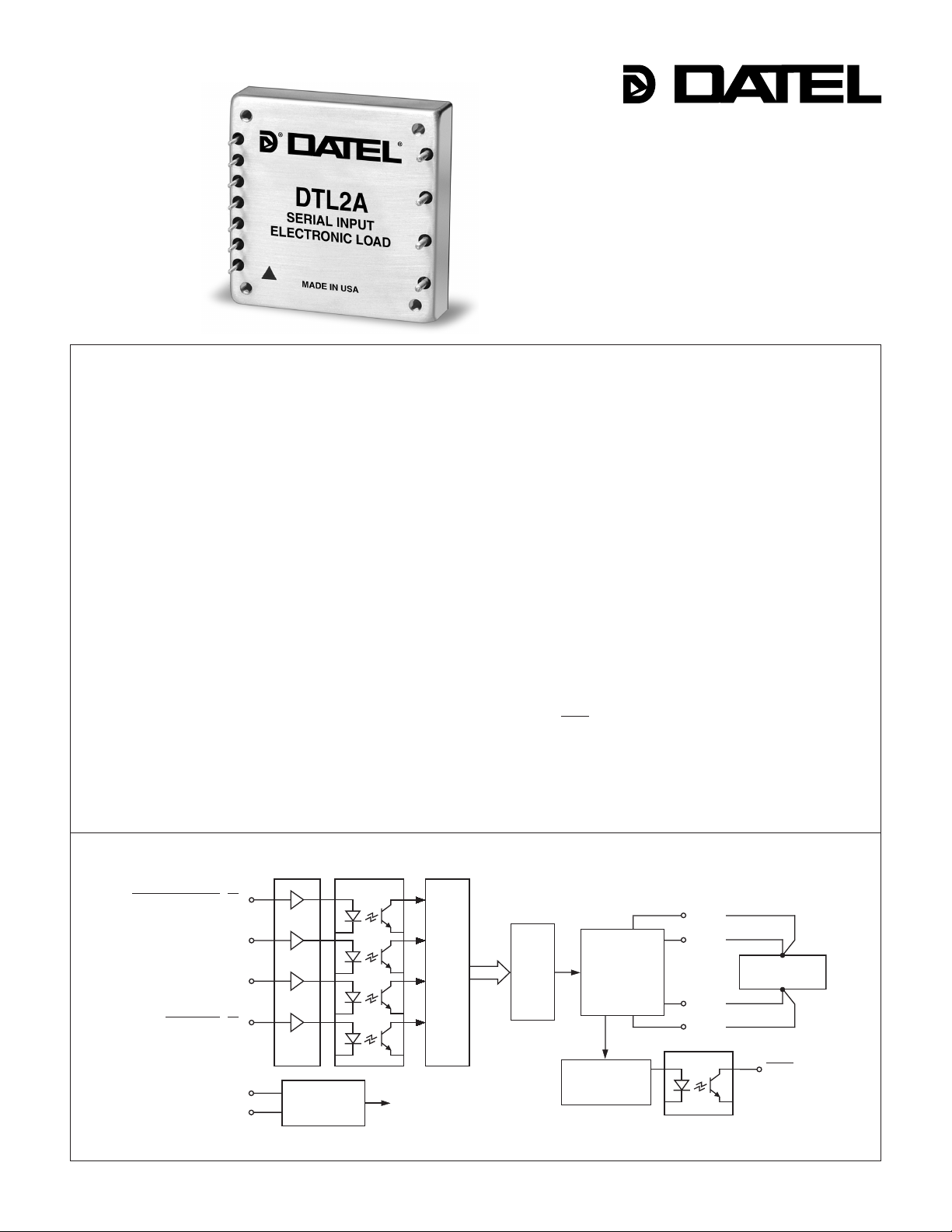
DATEL’s new DTL2A is an optically isolated, digitally programmable, serial-input,
electronic load. It is essentially a digitally controlled current source that can sink
currents from 0 to 20 Amps, at loading voltages from 2.5 to 50 Volts, up to a maximum
power of 100 Watts. The DTL2A is packaged in a thermally effi cient, 2" x 2" x 0.5"
metal package that incorporates an aluminum baseplate with through-hole spacers
for easy pcb mounting and/or external heat-sink attachment.
The DTL2A accepts a serialized, 12-bit, CMOS/TTL-compatible, digital input word
easily generated by any standard digital I/O card. The DTL2A buffers and then
optically isolates (500Vdc) the digital input data before storing it in a register and
presenting it to an on-board, 12-bit, digital-to-analog (D/A) converter. The D/A output
drives a near-ideal (10MΩ minimum output impedance), voltage-controlled current
source. One LSB (least signifi cant bit) of the D/A converter corresponds to a 5mA
increment (0.025% of 20A) in load current.
The DTL2A features a max. ±5mA offset error and a max. ±0.1% gain error. It
has an impressive full-scale step response time of 100µsec and can be operated
dynamically at update rates up to 20kHz. Powered by a single +5V supply, the DTL2A
draws a mere 150mA (maximum).
While operating in the constant-current mode up to 20 Amps (100W max. power),
the output compliance voltage of the DTL2A is 2.5 to 50 Volts. Should the output/load
voltage drop below the 2.5V minimum required for proper biasing, an internal monitoring
circuit activates the DTL2A's output Fault line. See DATEL’s DTL2A-LC for compliance
voltages as low as 0.6V.
DTL2A’s and other electronic loads, controller boards, and software from DATEL
are outstanding building-block components for power-supply burn-in and test systems.
They are an extremely reliable, cost-effective solution that enables you to quickly
confi gure impressively accurate systems.
INPUT
BUFFERS
CONTROL STROBE (CS)
CLOCK (CLK)
SERIAL DATA INPUT (SDI)
LATCH DATA (LD)
+5V SUPPLY
GROUND
DATEL, Inc., Mansfi eld, MA 02048 (USA) · Tel: (508)339-3000, (800)233-2765 Fax: (508)339-6356 · Email: sales@datel.com · Internet: www.datel.com
ISOLATED
DC/DC
CONVERTER
OPTO
ISOLATORS
DATA
LATCH
Figure 1. Simplifi ed Schematic
12-BIT
D/A
AMPLIFIER
AND
CURRENT
SENSOR
UNDERVOLTAGE
DETECTION
+LOAD
+LOAD
–LOAD
–LOAD
POWER DEVICE
UNDER TEST
FAULT
Page 2
DTL Series
0
100 WATT, SERIAL-INPUT ELECTRONIC LOADS
Performance Specifi cations and Ordering Guide
➀
Input Output
Compliance
Resolution Logic Current Resolution Voltage Power Package
Model (Bits) Compatibility (Amps) (mA)
➁ (Volts) ➂ (Watts) (Case, Pinout)
DTL2A 12 CMOS/TTL ➃ 0-20 5 2.5-50 0-100 C24, P31
➀ Typical at TA = +25°C with nominal +5V supply voltage unless noted.
➁ The smallest increment/decrement in output current is defi ned by one LSB (least signifi cant bit) of the 12-bit
digital input word. One LSB is equal to full scale (FS) divided by 4096 which corresponds to 0.0244% of 20A or 4.88mA.
➂ For proper operation, the unit's output/load voltage must remain within this range. Voltages greater than the listed
maximum can damage the device. Voltages less than the minimum provide insuffi cient bias for the output stage
and will result in unpredictable or no operation. See Output Compliance Voltage and the Fault Line for details.
➃ See Performance/Functional Specifi cations for details.
PART NUMBER STRUCTURE
DTL 2
DATEL
Electronic Load
A
A-Series
High Reliability
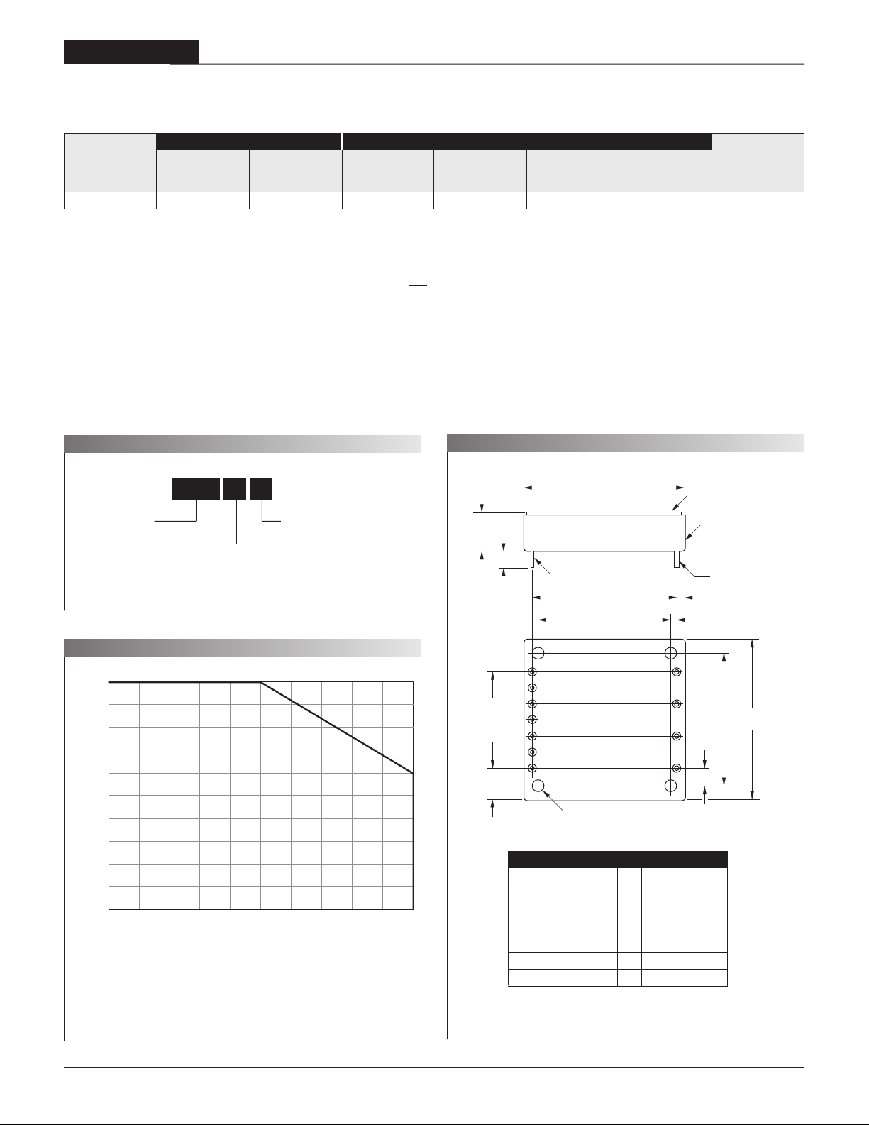
MECHANICAL SPECIFICATIONS
2.00
(50.80)
0.50
(12.70)
Case C24
ALUMINUM BASEPLATE
METAL CASE
Voltage Range:
2 = 2.5 to 50V
0.20 MIN
(5.08)
0.040 ±0.002 DIA.
(1.016 ±0.051)
1.800
(45.72)
1.640
(41.66)
0.060 ±0.002 DIA.
(1.524 ±0.051)
0.10
(2.54)
0.08
(2.03)
TEMPERATURE DERATING
10
11
BOTTOM VIEW
8
9
2.00
1.640
(50.80)
(41.66)
0.22
(5.59)
100
90
80
70
60
50
40
Output Power/Load (Watts)
30
20
10
010 203040506070809010
Baseplate Temperature (°C)
The horizontal axis of the above chart references the temperature of the DTL2A’s alumi-
num baseplate. The device can continually dissipate up to 100 Watts if the baseplate
7
6
1.20
(30.48)
6 EQ. SP. @
0.200 (5.08)
0.40
(10.16)
5
4
3
2
1
#4-40 CLEAR THRU
(TYP. 4 PL)
I/O Connections
Pin Function P31 Pin Function P31
1 Fault 7 Control Strobe (CS)
2 Ground 8 –Load
3 +5 Volt Supply 9 –Load
4 Latch Data (LD) 10 +Load
5 Serial Data In (SDI) 11 +Load
6 Clock (CLK)
is maintained at or below +50°C. At +25°C ambient temperature, with no heat sink or
supplemental air fl ow, the DTL2A can reliably dissipate a continuous 10 Watts.
Contact DATEL for Heat Sink information.
2
Page 3

100 WATT, SERIAL-INPUT ELECTRONIC LOADS
Performance/Functional Specifi cations
Typical @ TA = +25°C with nominal +5V supply voltage, unless noted.
Digital Inputs/Outputs
Logic Compatibility (Pins 1, 4-7) CMOS/TTL
Input Logic Levels:
Logic "1" +2 Volts, minimum
Logic "0" +0.8 Volts, maximum
Input Logic Loading:
Logic "1" (I
Logic "0" (I
Output Logic Levels:
Logic "1" (@ 150µA) +3.5 Volts, minimum
Logic "0" (@ 1.6mA) +0.4 Volts, maximum
Timing See Timing Diagram
Current:
Range 0-20 Amps
Resolution
Accuracy
Voltage Range ➁ 2.5-50 Volts
Power Range 0-100 Watts
Impedance 10MΩ, minimum
Offset Error
Gain Error ±0.1%, maximum
Isolation Voltage:
Digital Inputs/Output to ±Load 500Vdc, minimum
Any Pin to Case 500Vdc, minimum
Isolation Resistance 100MΩ, minimum
Output Slew Rate ±10A/µsec, minimum
Output Settling Time
Digital Input Update Rate to 20kHz
Power Supply Range (+VCC, Pin 3) +4.75-5.25 Volts (+5V nominal)
Power Supply Current 110mA typ., 150mA max.
Operating Temperature ➄ –40 to +100°C (Case)
Storage Temperature –40 to +125°C (Ambient)
Humidity (Non-condensing) to 95%
Altitude Above Sea Level 10,000 feet
Dimensions 2" x 2" x 0.5" (51 x 51 x 12.7mm)
Shielding 6-sided (Connected to pin 2)
Case Material Tin-plated steel shell with
aluminum baseplate
Pin Material Brass, solder coated
Mounting Holes Through-hole spacers, #4-40 clearance
Weight 1.9 ounces (54 grams)
IH @ VIH = 5 Volts) 20µA, maximum
IL @ VIL = 0 Volts) –0.6mA, maximum
Output
➀ 0.024%FS (4.88mA)
➅ ±1%, maximum
➂ ±5mA, maximum
Dynamic Performance
➃ 100µsec
Power Requirements
Environmental
Physical
DTL2A Model
➀ The smallest increment/decrement in output current is defi ned by one LSB (least signifi cant
bit) of the 12-bit digital input word. One LSB is equal to full scale (FS) divided by 4096 which
corresponds to 0.0244% of 20A or 4.88mA.
➁ For proper operation, the unit's output/load voltage must remain within this range. Voltages
greater than the listed maximum can damage the device. Voltages less than than the minimum
provide insuffi cient bias for the output stage and will result in unpredictable or no operation.
See Output Compliance Voltage and the Fault Line for details.
➂ Offset error is defi ned as the current sunk/sourced by the DTL2A’s output, under any output
voltage conditions, when the digital input word is all "0's."
➃ Full scale step (20 Amps) settling to within ±5mA of its fi nal value.
➄ See Temperature Derating.
➅ Applies over all specifi ed ranges/combinations of load voltage/current, operating temperature,
and V
CC.
Absolute Maximum Ratings
Power Supply Voltage (+VCC, Pin 3) –0.5 to +5.5 Volts
Digital Input Voltage (Pins 4-7) –0.5 to +5.5 Volts
Output Reverse-Polarity Protection No protection
Output Overvoltage Protection No protection
Output Undervoltage Protection Yes (See Fault Line)
Case Temperature +105°C
Storage Temperature (Ambient) –40 to +125°C
Lead Temperature (soldering, 10 sec.) +300°C
These are stress ratings. Exposure of devices to any of these conditions may adversely
affect long-term reliability. Proper operation under conditions other than those listed in the
Performance/Functional Specifi cations Table is not implied.
TECHNICAL NOTES
Overview
The DTL2A is a digitally programmable, CMOS/TTL-compatible, serial-input
current sink. It’s output/load current range is 0 to 20 Amps (in 4.88mA
increments), over a compliance voltage range of 2.5 to 50 Volts and an output/
load power range of 0 to 100 Watts. The device’s digital I/O coding is straight
binary (see table below). A digital input of all "0’s" forces a load current of 0
Amps. A digital input of all "1’s" forces a load current of 19.995 Amps.
In a typical power-supply test or burn-in application, the output pins of the
device under test (DUT) are connected to the DTL2A’s +Load (pins 10 and 11)
and –Load (pins 8 and 9) outputs. The DTL2A’s operation is controlled by its
four digital input lines (Serial Data In, Clock, Latch Data and Control Strobe).
Serial Input Data Word Load Current (Amps)
MSB LSB DTL2A
1111 1111 1111 19.995
1100 0000 0000 15.000
1000 0000 0000 10.000
0111 1111 1111 9.995
0100 0000 0000 5.000
0010 0000 0000 2.500
0000 0000 0001 0.005
0000 0000 0000 0.000
Mapping of the Serial-Input Data to Load Current
3
Page 4

DTL Series
100 WATT, SERIAL-INPUT ELECTRONIC LOADS
Initialization
Preparing the DTL2A to accept new digital data is accomplished by applying
logic "1's" to Control Strobe (CS, pin 7), Latch Data (LD, pin 4) and Clock
(CLK, pin 6) with all signals present and stable for a minimum of 1µsec.
During this interval, it does not matter whether or not data is present on the
Serial Data In (SDI, pin 5) line.
Serial Data
Following initialization, the 12-bit digital word representing the desired output
current is applied to the SDI pin. The serial data should appear starting with
the most signifi cant bit (MSB, bit 1, D11) and ending with the least signifi cant
bit (LSB, bit 12, D0). With each data bit present and stable on the SDI line,
the CLK must be toggled through a low-to-high transition to register that bit.
Twelve rising clock edges, at rates up to 500kHz, are required to clock all 12
digital bits into the DTL2A’s input register.
Latching Data and Presenting It to the D/A
After loading the LSB, the serial data word is latched by bringing the Control
Strobe (pin 7) high and then toggling the Latch Data pin (pin 4) through a
high-low-high sequence. Approximately 100µsec later, the output current will
settle to its fi nal desired value.
Software: C Language
The following steps describe a typical timing sequence when using the
DTL2A’s 4 digital inputs and a programming language such as C. Using 4 bits
of a typical 8-bit port, assign BIT_0 to the Control Strobe (CS, pin 7), BIT_1
to Latch Data (LD, pin 4), BIT_2 to Serial Data In (SDI, pin 5), and BIT_3
to the Clock (CLK, pin 6).
Output Compliance Voltage and the Fault Line
For proper operation, the DTL2A’s output/load voltage must always be
between 2.5 and 50 Volts. The device cannot be used to directly load low-
voltage, e.g. 1.8V or 2.5V, power components or to simulate a true short
circuit (0 Volts). Voltages greater than 50V can damage the device. Voltages
<2.5V will result in insuffi cient biasing of the output current source and
consequently unpredictable or no operation. Accordingly, we have installed
an internal output/load-voltage monitoring circuit. If the output/load voltage
drops below 2.5V and the DTL2A’s output is at risk of becoming disabled,
the Fault line activates.
The Fault line is an optically isolated, active-low function with an opencollector output (internal 10kΩ pull-up resistor to +5V). Under normal condi-
tions, its output is high (logic "1"). Under fault conditions (V
OUT < 2.5V), its
output drops to a logic "0." There is no output/load-voltage monitoring circuit
for voltages greater than 50V, and operation above 50V can damage the
device.
An "offset supply" can be inserted between the DTL2A’s –Load output (pins
8 and 9) and the power device under test (DUT) to "translate" the DTL2A’s
47.5V output/load voltage range. The offset supply must have adequate
current capabilities and be connected with the polarities indicated in Figure 2
below. Under no circumstances should the voltage across the DTL2A’s output
be allowed to experience a polarity reversal.
If a 5V/20A offset supply is inserted as shown, the range of DUT voltages
will be –2.5 to +45 Volts. Such a confi guration can be used for true short-
circuit testing. A mechanical relay can be used to short the outputs of the
DUT while the offset supply ensures the DTL2A always sees at least 5 Volts
across its outputs.
1. Initialize with Control Strobe, Latch Data, and Clock high:
BIT_0 = 1, BIT_1 = 1, BIT_2 = X (don’t care), BIT_3 = 1
2. Bring the Control Strobe low.
BIT_0 = 0
3. Apply the MSB (D11) of the serial data word to Serial Data In.
BIT_2 = 0 or 1
4. Toggle the Clock high-low-high.
BIT_3 = 1 to 0 to 1
5. Apply D10 of the serial data word to Serial Data In.
BIT_2 = 0 or 1
6. Toggle the Clock high-low-high.
BIT_3 = 1 to 0 to 1
7. Repeat the process for remaining data bits D9 through D0.
8. Drive the Control Strobe high.
BIT_0 = 1
9. Toggle the Latch Data input high-low-high.
BIT_1 = 1 to 0 to 1.
+LOAD
DTL2A
–LOAD
11
10
5V
9
8
Figure 2. An "Offset Supply" Enables
True Short-Circuit Testing
+
–
+
DUT
–
SHORT
CIRCUIT
RELAY
Thermal Considerations
The DTL2A can reliably handle 100W loads if its case temperature is
maintained at or below +50°C. With no heat sinking or auxiliary cooling, the
device can only handle loads up to 10 Watts. Please refer to the Temperature
Derating Curve for additional information. DATEL’s Electronic Load Applica-
tions Engineers can assist you in developing heat-sink solutions for your
higher-power DTL2A applications. Please contact us for details.
4
Page 5

E
100 WATT, SERIAL-INPUT ELECTRONIC LOADS
t
dh
DTL2A Model
CLK
CS
LD
SDI
D11 D10 D9 D8 D7 D6 D5 D4 D2D3 D1 D0
t
ds
t
in
t
t
css
t
ld1
cl
t
ch
Timing Min. Typ. Max. Units
CLK – – 500 kHz
tin 1 – – µsec
tcl = tch 1 – – µsec
tcss 1 – – µsec
tcsh 1 – – µsec
tld1 2 – – µsec
tld2 2 – – µsec
tldw 2 – – µsec
tds 0.5 – – µsec
tdh 0.5 – – µsec
t
csh
t
ld2
t
ldw
Figure 3. DTL2A Timing Diagram
®
INNOVATION and EX C ELL E N C
DATEL, Inc. 11 Cabot Boulevard, Mansfi eld, MA 02048-1151
Tel: (508) 339-3000 (800) 233-2765 Fax: (508) 339-6356
Internet: www.datel.com Email: sales@datel.com
DATEL makes no representation that the use of its products in the circuits described herein, or the use of other technical information contained herein, will not infringe upon existing or future patent rights. The descriptions contained herein
do not imply the granting of licenses to make, use, or sell equipment constructed in accordance therewith. Specifi cations are subject to change without notice. The DATEL logo is a registered DATEL, Inc. trademark.
®
ISO 9001 REGISTERED
DS-0450B 9/00
DATEL (UK) LTD. Tadley, England Tel: (01256)-880444
DATEL S.A.R.L. Montigny Le Bretonneux, France Tel: 01-34-60-01-01
DATEL GmbH München, Germany Tel: 89-544334-0
DATEL KK Tokyo, Japan Tel: 3-3779-1031, Osaka Tel: 6-354-2025
5
 Loading...