

Page 1
DTA1
Ordering number : EN2283B
1.0A Bidirectional Thyristor
Silicon Planar Type
SANYO Electric Co.,Ltd. Semiconductor Bussiness Headquarters
TOKYO OFFICE Tokyo Bldg., 1-10, 1 Chome, Ueno, Taito-ku, TOKYO, 110 JAPAN
O0797GI/3089MO, TS No.2283-1/3
Features
• Low AC power control use.
• Peak OFF-state voltage : 200 to 400V
• RMS ON-state current : 1A
• TO-92 package.
Absolute Maximum Ratings at Ta=25°C DTA1C DTA1E unit
Repetitive Peak V
DRM
200 400 V
OFF-StateVoltage
RMS ON-State Current I
T(RMS)
Tc=74°C, single-phase → 1.0 A
full-wave
Surge ON-State Current I
TSM
Peak 1 cycle, 50Hz → 8A
Amperes Squared-Seconds ∫ i2T·dt 1ms≤t≤10ms → 0.32 A2s
Peak Gate Power Dissipation P
GM
f≥50Hz, duty≤10% → 1W
Average Gate Power Dissipation P
G(AV)
→ 0.1 W
Peak Gate Current I
GM
f≥50Hz, duty≤10% → ±0.5 A
Peak Gate Voltage V
GM
f≥50Hz, duty≤10% → ±6 V
Junction Temperature Tj → 125 °C
Strage Temperature Tstg –40 to +125 °C
Weght → 0.2 g
Electrical Characteristics at Ta=25°C min typ max unit
Repetitive Peak I
DRM
Tj=25°C, VD=V
DRM
10 µA
OFF-State Current
Peak ON-State Voltage V
TM
ITM=1.5A 1.5 V
Holding Current I
H
VD=12V, gate open 10 mA
Gate Trigger Current* (I) I
GT
VD=12V, RL=20Ω 5mA
(II) I
GT
VD=12V, RL=20Ω 5mA
(III) I
GT
VD=12V, RL=20Ω 10 mA
(IV) I
GT
VD=12V, RL=20Ω 5mA
Gate Trigger Voltage* (I) V
GT
VD=12V, RL=20Ω 2V
(II) V
GT
VD=12V, RL=20Ω 2V
(III) V
GT
VD=12V, RL=20Ω 2–V
(IV) V
GT
VD=12V, RL=20Ω 2V
Gate Nontrigger Voltage V
GD
Tc=125°C, VD=V
DRM
0.2 – V
Thermal Resistance Rth(j-c) Between junction and case, AC 40 °C/W
* : The gate trigger mode is shown below.
Trigger mode T2 T1 G
I + – +
II + – –
III – + +
IV – + –
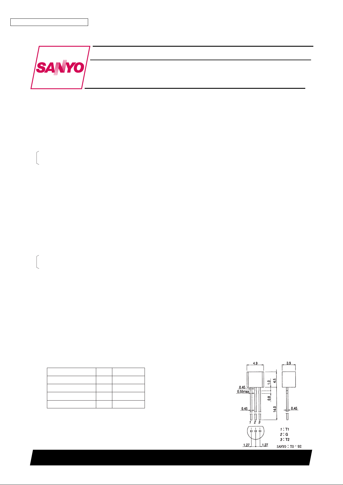
Package Dimensions 1192B
(unit : mm)
Page 2
DTA1
No.2283-2/3
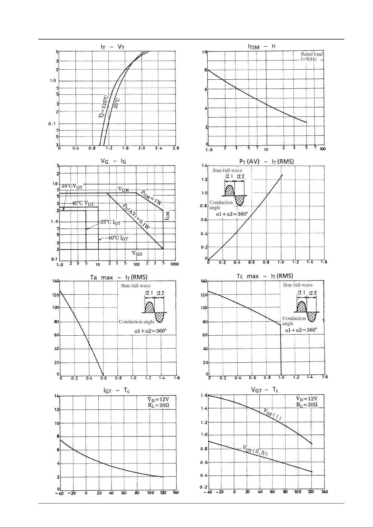
ON-State Voltage, VT– V
ON-State Current, I
T
– A
Gate Current, IG– V
Gate Voltage, V
G
– V
RMS ON-State Current, IT(RMS) – A
Average ON-State Power Dissipation, P
T
(AV) – W
RMS ON-State Current, IT(RMS) – A
Maximum Allowable
Case Temperature, Tc max – °C
Case Temperature, Tc – °C
Gate Trigger Voltage, V
GT
– V
Case Temperature, Tc – °C
Gate Trigger Current, I
GT
– mA
RMS ON-State Current, IT(RMS) – A
Maximum Allowable
Ambient Temperature, Ta max – °C
Number of Cycles at 50Hz, n
Surge ON-State Current, I
TSM
– A
Page 3

DTA1
No.2283-3/3
No products described or contained herein are intended for use in surgical implants, life-support systems,
aerospace equipment, nuclear power control systems, vehicles, disaster/crime-prevention equipment and
the like, the failure of which may directly or indirectly cause injury, death or property lose.
Anyone purchasing any products described or contained herein for an above-mentioned use shall:
Accept full responsibility and indemnify and defend SANYO ELECTRIC CO., LTD., its affiliates,
subsidiaries and distributors and all their officers and employees, jointly and severally, against any
and all claims and litigation and all damages, cost and expenses associated with such use:
Not impose any responsibilty for any fault or negligence which may be cited in any such claim or
litigation on SANYO ELECTRIC CO., LTD., its affiliates, subsidiaries and distributors or any of
their officers and employees jointly or severally.
Information (including circuit diagrams and circuit parameters) herein is for example only; it is not guaranteed for volume production. SANYO believes information herein is accurate and reliable, but no guarantees
are made or implied regarding its use or any infringements of intellectual property rights or other rights of
third parties.
This catalog provides information as of October, 1997. Specifications and information herein are subject
to change without notice.
Case Temperature, Tc – °C
Pulse Trigger Characteristic
Holding Current, I
H
– mA
Gate Trigger Pulse Width, tw– µs
I
GT
(tw) / I
GT
– %
Time, t – s
Transient Thermal Impedance, Rth(j-c) – °C/W
 Loading...