

Page 1
TRANSISTOR(PNP)
FEATURES
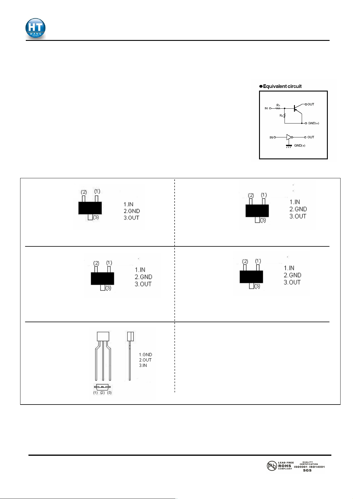
1. Built-in bias resistors enable the configuration of an inverter circuit without
connecting external input resistors(see equivalent circuit).
2. The bias resistors consist of thin-film resistors with complete isolation to
allow positive biasing of the input.They also have the advantage of almost
completely eliminating parasitic effects.
3. Only the on/off conditions need to be set for operation, making device
design easy.
PIN CONNENCTIONS AND MARKING
DTA114YE/DTA114YUA/DTA114YKA
/DTA114YSA/DTA114YCA
DTA114YE DTA114YUA
DTC114EUA
SOT-323
SOT-523
Addreviated symbol: 54
DTA114YKA DTA114YCA
SOT-23-3L
Addreviated symbol: 54
SOT-23
DTA114YSA
TO-92S
Addreviated symbol: 54
Addreviated symbol: 54
1
JinYu
semiconductor
www.htsemi.com
Date:2011/05
Page 2
DTA114YE/DTA114YUA/DTA114YKA
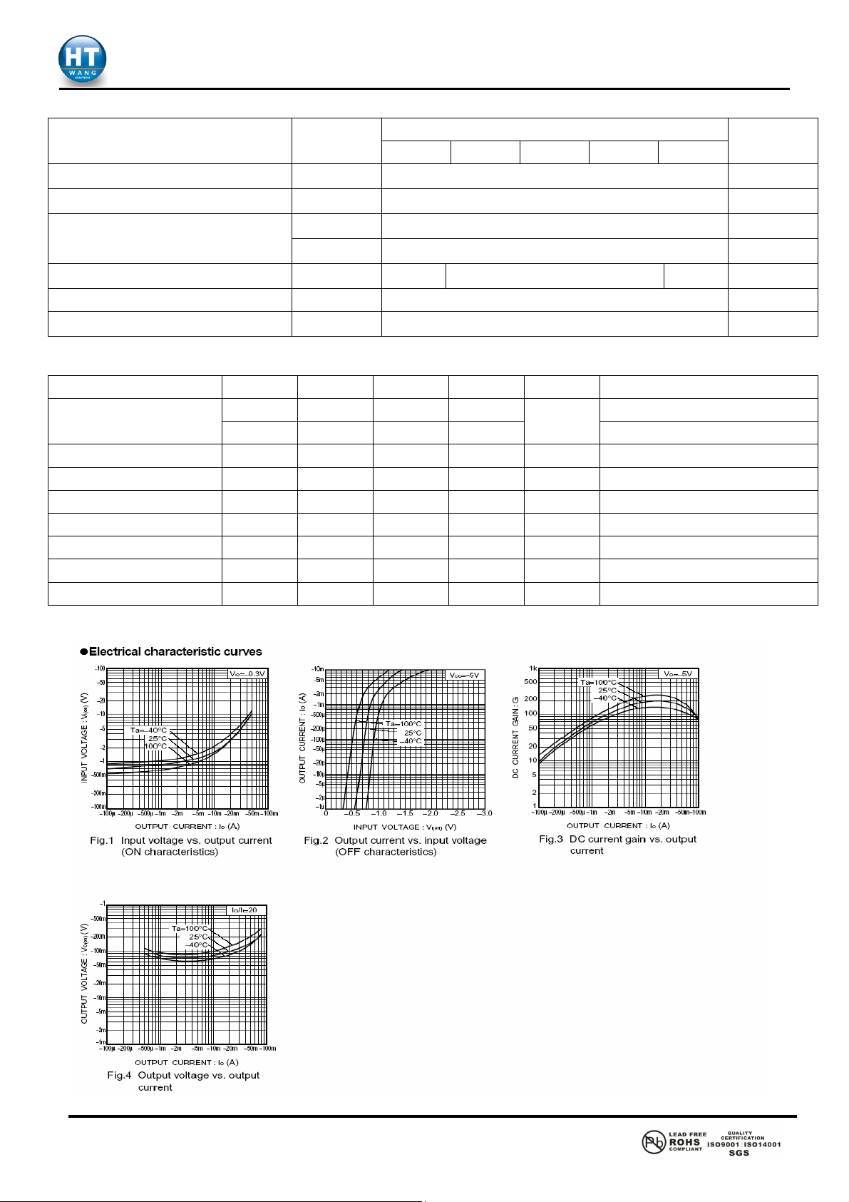
Absolute maximum ratings(Ta=25℃)
/DTA114YSA/DTA114YCA
Parameter Symbol
Limits (DTA114Y□ )
E UA KA CA SA
-50 V
Supply voltage
Input voltage
V
CC
-40to+6 V
V
IN
IO -70 mA
Output current
I
-100 mA
C(Max.)
150 200 300 mW
Power dissipation
Junction temperature
Storage temperature
Electrical characteristics (Ta=25℃
P
C
Tj 150
Tstg -55 to+ 150
)
Parameter Symbol Min. Typ Max. Unit Conditions
Input voltage
V
V
Output voltage
Input current
Output current
DC current gain
Input resistance
Resistance ratio
Transition frequency
Typical Characteristics
V
I
I
G
R
R
f
-0.3 VCC=-5V ,IO=-100µA
I(off)
-1.4
I(on)
-0.3 V IO/II=-5mA/-0.25mA
O(on)
-0.88 mA VI=-5V
I
-0.5 µA VCC=-50V ,VI=0
O(off)
68 VO=-5V ,IO=-5mA
I
7 10 13 KΩ
1
3.7 4.7 5.7
2/R1
250 MHz VO=-10V ,IO=5mA,f=100MHz
T
V
VO=-0.3V ,IO=-1mA
Unit
℃
℃
2
JinYu
semiconductor
www.htsemi.com
Date:2011/05
 Loading...