

Page 1
DTA114TE/DTA114TUA/DTA114TKA
/DTA114TSA/DTA114TCA
TRANSISTOR(PNP)
FEATURES
· Built-in bias resistors enable the configuration of an
inverter circuit without connecting ex temal input resistors.
· The bias resistors conisit of thin-film resistors with
complete isolation to allow positive biasing of the input.
They also have the advantage of almost completely
Eliminating parasitic effects.
· Only the on/off conditions need to be set for operation,
marking device design easy.
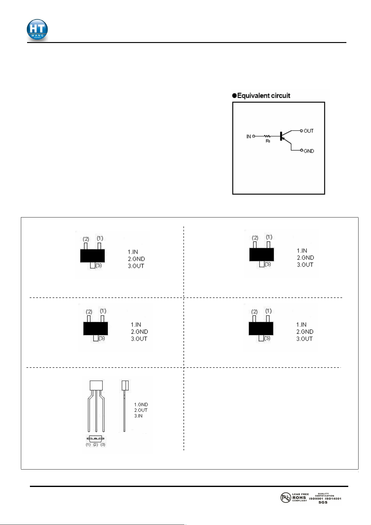
PIN CONNENCTIONS AND MARKING
DTA114TE DTA114TUA
(1) Base
(2) Emitter
(3) Collector
SOT-523
SOT-23-3L
DTA114TSA
TO-92S
Addreviated symbol: 94
Addreviated symbol: 94
SOT-323
DTA114ECA DTA114TCA DTA114TKA
SOT-23
Addreviated symbol: 94
(1) Base
(2) Emitter
(3) Collector
Addreviated symbol: 94
1
JinYu
semiconductor
www.htsemi.com
Date:2011/05
Page 2
DTA114TE/DTA114TUA/DTA114TKA
MAXIMUM RATINGS* TA=25 unless otherwise noted℃
Symbol Parameter
/DTA114TSA/DTA114TCA
LIMITS(DTA114T□)
E UA KA CA SA
Units
V
CBO
V
CEO
V
EBO
IC
PC
TJ, T
stg
Collector-Base Voltage
Collector-Emitter Voltage
Emitter-Base Voltage -5 V
Collector Current -Continuous -100 mA
Collector Dissipation 150 200 300 mW
Junction and Storage Temperature -55~+150 ℃
-50 V
-50 V
ELECTRICAL CHARACTERISTICS (Tamb=25℃ unless otherwise specified)
Parameter Symbol Test conditions MIN TYP MAX UNIT
Collector-base breakdown voltage
Collector-emitter breakdown
voltage
Emitter-base breakdown voltage
Collector cut-off current
Emitter cut-off current
DC current gain
Collector-emitter saturation voltage
Transition frequency
Imput resistor
V
(BR)CBO
V
(BR)CEO
V
(BR)EBO
I
CBO
I
EBO
h
V
CE(sat)
R1 7 10 13
FE
I
f
T
VCE=-10V,IC=-5mA, f=100MHz
Ic=-
Ic=-
=-
I
E
VCB=-50V,IE=0
V
EB
=-5V,IC=-1mA
V
CE
=-10mA,IB=-1mA -0.3 V
C
50µ
A,IE=0
1mA,I
=0
B
A,IC=0
50µ
=-4V,IC=0
-50 V
-50 V
-5 V
-0.5 uA
-0.5 uA
100 250 600
250 MHz
kΩ
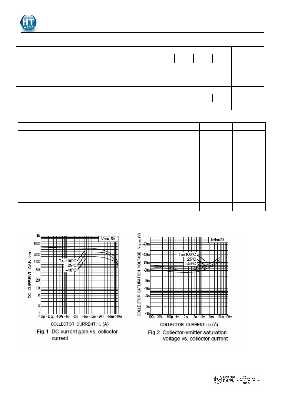
Typical Characteristics
2
JinYu
semiconductor
www.htsemi.com
Date:2011/05
 Loading...